Note : Les descriptions sont présentées dans la langue officielle dans laquelle elles ont été soumises.
CA 02391130 2002-05-09
WO 02/25745 PCT/ILO1/00828
SEMICONDUCTOR NANOCRYSTALLINE MATERIALS
AND THEIR USES
Field of the Invention
The invention relates to new semiconductor composite nanocrystal materials
having desirable luminescent properties, specifically high quantum yields and
good photochemical stability with specific, desirable emittance wavelengths,
and their various applications in optical, electrical, electro-optical and
laser
devices particularly in the field of telecommunication.
Background of the Invention
Semiconductor nanocrystals have been extensively investigated, since it is
well known that the properties of the materials in this form, differ
substantially from those of the bulk solid. The wavelength of light emitted
from semiconductor nanocrystal quantum dots is tunable by their size as a
result of the quantum-confinement effect [Nirmat et al., Acc. Chem. Res. 1999,
32, 407; Alivisatos A. P., Science 1996, 271, 933; Weller H., Angew. Chem.
Int.
Ed. Engl. 1993, 32, 41; Banin U., et al., Nature 1999, 400, 542]. Harnessing
this emission for applications such as biological fluorescence marking,
[Bruchez M., et al., Science 1998, 281, 2013; Chan W.C.W., et al., Science
1998, 281, 2016; Mitchell G.P., et al., J. Am. Chem. Soc. 1999 121, 8122]
optoelectronic devices, and lasers [Colvin V.L., et al., Nature 1994, 370,
354;
Dabboussi B.O., et al., Appl. Phys. Lett. 1995, 66, 1316; Schlamp, M.C., et
al.,
CA 02391130 2002-05-09
WO 02/25745 PCT/ILO1/00828
-2-
J. Appl. Phys. 1997, 82, 5837; Mattoussi H., et al., J. Appl. Phys. 1998, 83,
7965] is challenging since stringent requirements are imposed. These include
a high fluorescence quantum yield (QY), and stability against
photo-degradation. The required characteristics have proven difficult to
achieve in semiconductor nanocrystals coated by organic ligands, due to
imperfect surface passivation. In addition, the organic ligands are labile for
exchange reactions because of their weak bonding to the nanocrystal surface
atoms [Kuno M., et al., J. Chem. Phys. 1997, 106, 9869]. A pxoven strategy for
increasing both the fluorescence QY and the stability of nanocrystals, while
maintaining the solubility and chemical accessibility of the sample, is to
grow
a shell of a higher band gap semiconductor on the core nanocrystal, and for
II-VI semiconductor nanocrystals, core/shell structures have been successfully
developed, including the successful synthesis of highly emitting CdSe/ZnS
nanocrystals. The synthesis of this material employs a high temperature route
in trioctylphosphine (TOP)/trioctylphosphineoxide (TOPO) solution. Another
approach employing a low temperature route has been used to grow CdSe/CdS
corelshells in pyridine. These core/shell nanocrystals are still overcoated
with
outer organic ligands that maintain their solubility and chemical
accessibility.
They fluoresce in the visible range with a QY of 30-90%, and have increased
photochemical stability [Nines, M. A., et al., J. Phys. Chem. 1996, 100, 468;
Peng, X., et al., J. Am. Chem. Soc. 1997, 119, 7019; Dabbousi, B.O., et al.,
J.
Phys. Chem. B. 1997, 101, 9463; Tian, Y., et al., J. Phys. Chem. 1996, 100,
8927; Cao, Y.W., et al., Angew. Chem. Int. Ed. Engl. 1999, 38, 3692].
CA 02391130 2002-05-09
WO 02/25745 PCT/ILO1/00828
-3-
In most previously fabricated composite core/shell combinations, both the
shell
material type and the shell thickness affected the optical and electronic
properties of the semiconductor nanocrystals. .Although this potentially
provides extra degrees of freedom in tailoring the optical, electronic,
electrical
and chemical properties of semiconductor nanocrystals, the effect of shell
type
and thickness on wavelength emitted by the composite nanocrystal makes
control during fabrication and long term stability of the characteristic
wavelength of components manufactured from these materials difficult to
achieve. It is noteworthy that most prior art core/shell combinations emit at
visible and shorter wavelengths, whereas for telecommunications applications,
near infra-red (NIR) emittances are technologically desirable as data carrying
signals.
In modern data communication systems NIR optical signals including laser
signals are modulated by the data to be transmitted, and are required to be
carried from a first point to a second point, propagating along an optical
fiber
that connects the said two points. The magnitude of these data-carrying
optical signals is attenuated as they travel along the optical fiber due to
various losses, and therefore the signals require amplification by optical
amplifiers located at predetermined points along the fiber. Conventional
optical amplifiers suffer from limited tunability of both center-frequency and
bandwidth, which is a major drawback. This limitation results from the fact
that the amplification means employed by conventional optical amplifiers and
CA 02391130 2002-05-09
WO 02/25745 PCT/ILO1/00828
-4-
transmitters is a plurality of individual doping atoms with limited available
optical transitions.
Thus for a variety of telecommunication purposes there is a need for materials
having emittance and optical gain as well as laser action, tunable in the Near
IR (NIR) spectral range. This tunability will enable adjustment of the
bandwidth and central frequency for optical amplification of a plurality of
data
carrying signals and their transmission around a stable center-frequency.
InAs nanocrystals can provide the flexibility required for this purpose. It
has
been demonstrated that it is possible to tune the band gap fluorescence of
this
material over the range of 800-1500 nm by varying the nanocrystal radii over
the range 1-4 nm. However, the quantum yield flY of this material is low, and
at room temperature it is limited to a mere 0.5-2%. These InAs nanocrystals
are also easily degraded by oxidation and lack photo-stability. One known
method of overcoming these, and other problems is to coat the nanocrystal
with an appropriate shell, for example, CdS shells have been successfully
applied to CdSe cores [Peng X. et al. ibid. 1997].
Whilst overcoming the stability limitations that are inherent to the
non-shelled InAs, the band gap of previously disclosed shell materials
generally modified the luminescence wavelength of the core nanomaterial
(Cao, Y.W., et al ibid.J. Indeed applying a shell with a bandgap close to that
of
the core is a further known means of modifying the luminescence wavelengths
CA 02391130 2002-05-09
WO 02/25745 PCT/ILO1/00828
of nanocrystals, and, although this potentially provides extra degrees of
freedom in achieving speci~.c emission wavelengths, the partial dependency of
the emission wavelength of core/shell nanomaterials on the shell material and
its dimensions makes control of this critical parameter during fabrication
more difficult, as two extra process variables are introduced. The long-term
stability in emission wavelength may also be detrimentally affected as
changes in the outer layers of the shell can affect the wavelength of light
emitted, and these outer layers interface with the environment and are thus
susceptible to degradation processes in the course of time (aging).
Nevertheless, high quantum yields are attainable with core/shell
nanocrystals, and in a previous publication [Cao Y.W. and Banin U., Angew.
Chem. Int. Ed. Engl. 1999, 38, 3692], the present inventors reported the
growth of InAs/InP and InAS/CdSe core/shells. InP and CdSe shell materials
have low lattice mismatches and small conduction band offsets compared with
the core material. Thus, while it was not surprising that shells of these
materials could be grown onto InAs cores, it was surprising that an impressive
20-fold enhancement of the room temperature QY to 20% was obtained for
InAs/CdSe: Indeed this is better than the quantum yields of traditional
organic NIR laser dyes.
Various manufacturing routes have been used for manufacturing
semiconductor nanocrystals. The colloidal chemical route is widely applicable
for synthesis of a variety of II-VI semiconductor nanocrystals such as CdSe
[hurray, C.B., et al., J. Am. Chem. Soc. 1993, 115, 8706], as well as for III-
V
CA 02391130 2002-05-09
WO 02/25745 PCT/ILO1/00828
semiconductors such as InP [Micic, O.L, et ccl., J. Phys. Chem. 1994, 98,
4966;
Nozik, A.J., et al., MRS Bull. 1998, 23, 24; Guzelian, A.A., J. Phys. Chem.
1996, 100, 7212] and InAs [Guzelian, A.A., et al., Appl. Phys. Lett. 1996, 69,
1462].
A specific known method uses a solution pyrolytic reaction of organometallic
precursors in trioctylphosphine (TOP) [Peng, X., et al., A. P. J. Am. Chem.
Soc.
1998, 120, 5343], and using this method, band gap' - fluorescences tunable
between 800-1400 nm for radii ranging between 1 to 4 nm respectively, were
observed, but the QY at room temperature was limited to 0.5-2%. The limited
QY has been attributed to the surface passivation of the nanocrystals, which
are overcoated by TOP ligands. TOP is a Lewis base that preferentially binds
to cationic indium sites on the nanocrystal surface. This, along with the
steric
hindrance that the bulky TOP ligands impose on neighboring nanocrystal
surface sites, leads to incomplete electronic passivation of surface dangling
orbitals. The presence of such sites provides efficient pathways for
nonradiative decay of the nanocrystal excited state, limiting the maximum
fluorescence QY. Whereas the poor quantum yield can be improved by
application of a shell, to date, such encapsulation has always modified the
emission wavelengths in III-V cored nanocrystals.
It is an object of the present invention to provide core/shell nanocrystals
that
overcome the drawbacks of prior art crystals.
CA 02391130 2002-05-09
WO 02/25745 PCT/ILO1/00828
_7_
It is a particular object of the present invention to provide optically and
chemically stable nanocrystals that luminesce at I~TIR wavelengths and that
would be useful in various applications.
It is a further object of the present invention to provide a method for
producing epitaxially grown shells as a means of encapsulating III-V
semiconductor nanocrystals, thus forming core/shell nanocrystals such that
the luminescent wavelength of said core/shell nanocrystals will depend on the
dimensions and properties of the core, and will be substantially independent
of the thickness and material of the shell.
It is a further object of the invention to provide a process for production of
novel core/shell nanocrystals having III-V semiconductor cores, such materials
including, but not being limited to InAs/GaAs, InAs/ZnS and InAs/ZnSe.
It is still another object of the invention to provide an efficient optical
amplifier having a stable bandwidth using core shell nanocrystals.
It is still another .object of the invention to provide lasers using
core/shell
nanocrystals.
It is yet another object of the invention to provide efficient wideband
optical
ampli~.ers and lasers having adjustable center-frequency and bandwidth.
CA 02391130 2002-05-09
WO 02/25745 PCT/ILO1/00828
_$_
These and other objects of the invention will become clearer as the
description
proceeds.
Summary of the Invention
The present invention relates to a semiconductor core/shell nanocrystal
comprising a semiconductor nanocrystal core that is luminescent in the near
infra red (NIR), and having a crystalline shell encapsulating said core, said
shell having a bandgap and/or crystallographic structure such that emittance
wavelength of the core material encapsulated therein is substantially not
modified, said core/shell nanocrystal having a changed quantum yield and/or
chemical and/or photostability that is different from that of the
non-encapsulated nanocore. The core/shell nanocrystal are usually coated with
organic ligands of various types such as phosphines, amines and thiols, on the
outer surface, and the ligands can be substituted or removed.
The semiconductor core/shell nanocrystals of the invention preferably have a
semiconductor core consisting of InAs or InSb.
In a particular embodiment of the semiconductor core/shell nanocrystal of the
invention, the core is a complex nanocrystalline core comprising a first canon
species and a first anion species and at least one additional ionic species
which
may be cationic or anionic, the ratio of total cationic species to total
anionic
species being substantially equimolar. The said cationic species may be
CA 02391130 2002-05-09
WO 02/25745 PCT/ILO1/00828
_g_
selected from In, Ga or A1 and said anionic species islare selected from As,
Sb
and P.
In the semiconductor core/shell nanocrystals of the invention the core may
further comprise at least one additional species at dopant concentration. Such
additional species may be a rare-earth element, for example a trivalent
rare-earth element such as Er.
In the semiconductor core/shell nanocrystals of the invention the shell
comprises a first cationic species and a first anionic species at a
substantially
equimolar ratio. The said first cationic species may be Zn and the said first
anionic species may preferably be selected from sulphur or Se. Alternatively,
the said first cationic species may be Ga and the said first anionic species
may
be selected from As and P.
These semiconductor core/shell nanocrystals may have shell that is a complex
nanocrystalline shell, that comprises a first cationic species and a first
anionic
species and at least one additional ionic species which may be cationic or
anionic; the ratio of total cationic species to total anionic species being
substantially equimolar. The said cationic species may be selected from Zn,
Cd, Ga, A1 and In and the said anionic species may be selected from sulphur,
Se, As, and P. The shell of these semiconductor core/shell nanocrystals may
further comprise additional species at dopant concentrations. The said
CA 02391130 2002-05-09
WO 02/25745 PCT/ILO1/00828
-10-
additional species may be a rare-earth element, particularly a trivalent
rare-earth element such as Er.
The semiconductor core/shell nanocrystal of the invention preferably have
emittance of a wavelength of from about 0.8 microns to about 2 microns, and
preferably from 1.1 microns to 1.6 microns. Particular semiconductor
core/shell nanocrystals according to the invention have an emittance
wavelength of about 1.3 microns.
In another embodiment the invention relates to a method for the preparation
of core/shell nanocrystals comprising an InAs nanocore encapsulated in a
shell, comprising the steps of (a) preparing a first stock precursor solution
of
In:As for nanocrystal cores having a molar ratio of In:As to nucleate InAs
nanocrystals therefrom; (b) preparing a second stock precursor solution of a
shell material; (c) injecting said first stock precursor solution at room
temperature into TOP or TOP/TOPO solution at elevated temperature to
nucleate core nanocrystals, with addition of further stock precursor solution
as
necessary, to achieve desired core dimensions; (d) precipitating core
nanocrystals; and (e) contacting the nanocrystals obtained in step (d) with
said second stock precursor solution of shell material to allow for growth of
said shell on said core; the temperature for shell growth being a relatively
high temperature of above about 130°C and up to about 400°C, the
molar ratio
of cation:anion being from about 4:1 to about 1:1 and the reactants being
dissolved in a TOP/TOPO combination. The nanocrystals obtained by the
CA 02391130 2002-05-09
WO 02/25745 PCT/ILO1/00828
-11-
method of the invention usually have organic ligands as a coating on their
outer surfaces. Such organic ligands contribute to maintaining the solubility
and chemical accessibility of the samples. The organic ligands may be
substituted or removed In the method of the invention, the first precursor
stock solution of InAs cores preferably contains In:As at a molar ratio of
from
about 1:2 to about 1:1.5. The said shell material may be GaAs and said second
precursor stock solution contains As:Ga at a molar ratio of about 1:4. The
said
shell material may alternatively be ZnSe, where said second stock precursor
solution contains Zn:Se at substantially equimolar ratio. Still alternatively
the
said shell material may be ZnS, where said second stock precursor solution
contains S:Zn at substantially equimolar ratio.
In a still further embodiment, the invention relates to a wideband optical
amplifier for amplifying data-carrying optical signals, comprising a plurality
of semiconductor core/shell nanocrystals, wherein each of said core/shell
nanocrystals has core dimensions that correspond to a specific optical band
and is located at a predetermined point within a light transmitting medium;
and a pumping, coherent-light source connected to said light transmitting
medium for exciting each of said nanocrystals with light energy required for
the amplification of data-carrying optical signals within said specific
optical
band, received in said light transmitting medium. The said light-transmitting
medium is preferably a segment of optical fiber.
CA 02391130 2002-05-09
WO 02/25745 PCT/ILO1/00828
-12-
In the wideband optical amplifier according to the invention the said
semiconductor core/shell nanocrystals are preferably comprised of a
nanocrystal core that is luminescent, preferably in the near infra red (NIR),
and has a shell encapsulating said core, said shell having a bandgap and/or
crystallographic structure such that emittance wavelength of the core
material encapsulated therein is substantially not modified, said corelshell
nanocrystal having increased quantum yield and increased chemical and/or
photostability relative to the non-encapsulated nanocore.
The present wideband optical amplifier may employ any nanocrystal in
accordance with the present invention.
In an additional embodiment, the invention relates to an optical data
communication system, comprising a modulator, connected to a data-source,
for modulating at least one optical signal with data to be carried from said
data-source to a destination, by said at least one optical signal; at least
one
wideband optical amplifier of the invention for amplifying data-carrying
optical signals; a demodulator, located at said destination, for demodulating
said data-carrying optical signals; a first segment of light transmitting
medium, for connecting between said modulator and said at least one
wideband optical amplifier; segments of light transmitting medium, for
connecting between said at least one wideband optical amplifier and
subsequent at least one amplib.ers; and a second segment of light transmitting
medium, for connecting between the last wideband optical ampli~.er and said
CA 02391130 2002-05-09
WO 02/25745 PCT/ILO1/00828
-13-
demodulator. The said light transmitting medium is preferably an optical
fiber.
In another embodiment the invention relates to a core/shell nanocrystal laser
comprising: a laser host medium, a plurality of semiconductor core/shell
nanocrystals uniformly dispersed in the laser medium host, a pumping source
for exciting each of the nanocrystals, an optical cavity providing an optical
feedback mechanism for the coherent light produced by the laser active
medium in the laser host medium, and optionally, if necessary, a cladding
layer on the surface of the laser host medium to provide a channel wave guide.
In the laser according to the invention, the semiconductor core/shell
nanocrystals are preferably comprised of a nanocrystal core that is
luminescent, preferably the near infra red, and has a shell encapsulating the
core. The shell having a bandgap and/or crystallographic structure such that
emittance wavelength of the core material encapsulated therein is
substantially not modified. The core/shell nanocrystal having increased
quantum yield and increased chemical and/or photostability relative to the
non-encapsulated nanocore, wherein the nanocrystal may be coated with
organic ligand on the outer surface thereof.
The present laser may employ any nanocrystal in accordance with the present
invention.
CA 02391130 2002-05-09
WO 02/25745 PCT/ILO1/00828
-14-
In a preferred embodiment, the invention relates to a laser with emission in
the NIR spectral range. In such a laser, the core/shell nanocrystals are used
as
the active laser medium, in solution, or in other media such as a film, a
solid
host such as a polymer or a segment of an optical fiber. In preferred
embodiments of the laser of the invention, the solvent is an organic solvent,
preferably either hexane or toluene.
In a further embodiment of the laser of the invention, the optical cavity is a
cylindrical microcavity comprising a capillary tube with a segment of an
optical fiber inserted through its center and the laser host medium is an
organic solvent, occupying the region between the fiber and outer capillary
tube in which a plurality of semiconductor core/shell nanocrystals are
uniformly dispersed in solution.
In yet another embodiment, the invention relates to a laser active medium
comprising a plurality of semiconductor corelshell nanocrystals uniformly
dispersed in a laser host medium host.
In the laser active medium of the invention the semiconductor core/shell
nanocrystals are preferably comprised of a nanocrystal core that is
luminescent, preferably in the near infra red, and has a shell encapsulating
the core. The shell having a bandgap and/or crystallographic structure such
that emittance wavelength of the core material encapsulated therein is
substantially not modified. The core/shell nanocrystal having increased
CA 02391130 2002-05-09
WO 02/25745 PCT/ILO1/00828
-15-
quantum yield and increased chemical and/or photostability relative to the
non-encapsulated nanocore, wherein the nanocrystal may be coated with
organic ligand on the outer surface thereof.
The present laser active medium may employ any nanocrystal in accordance
with the present invention.
In the present laser active medium the nanocrystyals are uniformly dispersed
in a host medium that is preferably selected from a film, an optical fiber, a
polymeric hlm, or an organic solvent. The organic solvent is preferably either
hexane or toluene.
Brief Description of the Drawings
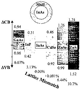
Figure 1: Summary of the band offsets (in eV) and lattice mismatch (in %)
between the core InAs and various III-V semiconductor shells (left side), and
II-VI semiconductor shells (right side). CB = conduction band; VB = valence
band.
Figure 2: Evolution of the absorption spectra during the growth of InP shells
on InAs cores with an initial radius of 1.3 nm. The InP shell thickness in
number of monolayers is: (a) 0, (b) 0.5, (c) 1.1, (d) 1.7, (e) 2.5.
CA 02391130 2002-05-09
WO 02/25745 PCT/ILO1/00828
-16-
Figure 3: Evolution of absorption (dashed lines), and photoluminescence
(solid line) for growth of core/shells. The PL spectra are given on a relative
scale for comparison of the enhancement of QY with shell growth.
A. InAs/CdSe with initial core radius of 1.2 nm. The shell thickness (in
number of monolayers) and QY for the traces from bottom to top are
respectively: 0, 1.2%; 0.6, 13%; 1.2, 21%; 1.8, 18%.
B. InAs/CdSe with initial core radius of 2.5 nm. The shell thickness (in
number of monolayers) and QY for the traces from bottom to top are
respectively: 0, 0.9%; 0.7, 11%; 1.2, 17%; 1.6, 14%.
C. InAs/ZnSe with initial core radius of 1.2 nm. The shell thickness (in
number of monolayers) and QY for the traces from bottom to top are
respectively: 0, 1.2%; 0.6, 9%; 1.5, 18%; 2.5, 14%.
D. InAs/ZnSe with initial core radius of 2.8 nm. The shell thickness (in
number of monolayers) and QY for the traces from bottom to top are
respectively: 0, 0.9%; 0.7, 13%; 1.3, 20°/; 2.2, 15°/.
E. InAs/ZnS with initial core radius of 1.2 nm. The shell thickness (in
number of monolayers) and QY for the traces from bottom to top are
respectively: 0, 1.2%; 0.7, 4%; 1.3, 8%; 1.8, 7%.
F. InAs/ZnS with initial core radius of 1.7 nm. The shell thickness (in
number of monolayers) and QY for the traces from bottom to top are
respectively: 0, 1.1%; 0.6, 5%; 1.3, 7.1%; 2.2, 6.3%.
Figure 4: XPS survey spectrum for InAs cores with radius of 1.7 nm (lower
trace), and for InAs/CdSe core/shells with shell thickness of 3 monolayers
(top
CA 02391130 2002-05-09
WO 02/25745 PCT/ILO1/00828
-17-
trace). The assignment of the peaks is indicated. The new peaks in the XPS
spectrum for the core/shells associated with Cd and Se are emphasized in bold
italic type.
Figure 5: Summary of high resolution XPS data for InAs/ZnSe and InAs/InP
core/shells.
A. For InAs/ZnSe core/shells, the log of the ratio of the intensities of the
Incas to the In~rrr is shown, versus the shell thickness.
B. For InAs/InP core/shells, the log of the ratio of intensities of the Incas
to
Assa is shown, versus the shell thickness. In both cases the ratio is
normalized
to the ratio in the cores. Squares: experimental data. Solid line: calculated
ratio for core/shell structure. Dotted line: calculated ratio for alloy
formation.
Figure 6: HRTEM images of InAs/InP core/shell (frame A, core radius 1.7 nm,
shell thickness 2.5 nm), InAs core (frame B, core radius 1.7 nm), and
InAs/CdSe core/shell (frame C, core radius 1.7 nm, shell thickness 1.5 nm).
The scale bar is 2 nm. The nanocrystals are viewed along the [011] zone axis.
Frame D shows the Fourier transform of image C, and the pattern
corresponds to the diffraction pattern from the 011 zone of the cubic crystal
structure.
Figure 7: TEM images of InAs/InP core/shells (frame A, core radius 1.7 nm,
shell thickness 2.5 nm), InAs cores (frame B, core radius 1.7 nm), and
InAs/CdSe core/shells (frame C, core radius 1.7 nm, shell thickness 1 nm). The
CA 02391130 2002-05-09
WO 02/25745 PCT/ILO1/00828
-18-
scale bar is 50 nm. The inset of frame B (70x70 nm), displays a portion of a
superlattice structure formed from the InAs cores.
Figure 8: XRD patterns for InAs cores with radius of 1.7 nm (trace A, solid
line), and InAs/InP core/shells with shell thickness of 2.4 monolayers (B,
dashed line), and 6.2 monolayers (C, dot-dashed line). The inset shows a zoom
of the 111 peak. The diffraction peak positions of bulk cubic InAs (dark) and
InP (light, italic) are indicated.
Figure 9: X-ray diffraction patterns for InA.s cores and various core shells.
The experimental curves (filled circles) are compared with the simulated
curves (thin solid lines). The markers on the bottom of each frame indicate
the
diffraction peak positions and the relative intensities for the InAs core
material (lower frame), and the various shell materials (other traces). The
vertical dashed lines indicate the positions of the InAs core nanocrystal
diffraction peaks.
Figure 10: Experimental and calculated shifts of the band gap energy in
various core/shells versus the shell thickness. InAsIZnS core/shells:.
experimental data - squares, calculated shift of gap - dot-dashed line.
InAs/InP core/shells: experimental data - circles, calculated shift of gap -
dashed line. InAs/GdSe core/shells: experimental data - triangles, calculated
shift of gap - solid line.
CA 02391130 2002-05-09
WO 02/25745 PCT/ILO1/00828
-19-
Figure 11: Comparison of stability of cores (frame A), InAs/CdSe core/shells
(frame B), and InAs/ZnSe core/shells (frame C). Absorption spectra (solid
lines) and PL spectra (dashed lines) are shown on the same energy scale for
fresh (bottom traces in each frame), and for nanocrystals kept in an oxygen
saturated solution for 10 months (top traces in each frame). The
Photoluminescence QY is also indicated in each case.
Figure 12: Optical gain measurement in a close packed film of core/shell
nanocrystals using the variable stripe method.
A. Schematically shows the experimental arrangement.
B. The logarithm of the intensity of the emission from the stripe plotted
versus the illuminating stripe length. The points and solid line are the
experimental points, and the dashed line is a fit to the portion exhibiting
optical gain.
Definitions
The term nanocrystal as used herein refers to a single crystal particle of
dimensions about 15 - 300 Angstroms, typically 20 - 100 Angstroms.
The terms "Near Infra Red" and "NIR" as used herein refer to light in the
wavelength range of about 0.8-4.3 microns, but specifically 0.8 - 2 microns.
CA 02391130 2002-05-09
WO 02/25745 PCT/ILO1/00828
-20-
The term "semiconductor nanocrystal" as used herein refers to nanocrystal of
Group III-V or II-VI, or core/shell nanocrystal where core and shell are made
from Group III-V or Group II-VI compounds.
The term "ionic species" as used herein refers to atoms in the semiconductor
crystal lattice that are formally positively or negatively charged, regardless
of
the actual degree of covalency exhibited by the interatomic bonding.
The term "cationic species" as used herein refers to atoms in the
semiconductor crystal lattice that are formally positively charged.
The term "anionic species" as used herein refers to atoms in the semiconductor
crystal lattice that are formally negatively charged.
The term "alloy" and variations thereof, as used herein refers to a complex
nanocrystalline material having mixed atomic species, with either a plurality
of cationic species or a plurality of anionic species (or both) co-
precipitated out
of solution, and deposited within the same layer of the nanocrystalline
lattice.
Thus an alloyed nanocrystalline core is a core such as InAsP, and an alloyed
nanoshell is a shell such as ZnSSe.
CA 02391130 2002-05-09
WO 02/25745 PCT/ILO1/00828
-21-
Detailed Description of the Invention
The present invention relates to corelshell nanocrystals that are based on a
new concept for obtaining high quantum yield, stable Near Infra Red
luminescent emitters for telecommunications applications. It is proposed to
use a shell with a very different bandgap from that of the core as a means for
encapsulating reactive cores, protecting them against chemical attack such as
oxidation, thereby increasing chemical stability and quantum yield, whilst
maintaining the luminescence wavelengths characteristic of the core. The
range of wavelengths obtainable will thus depend only on the core material
and its radius, due to the quantum-confinement effect, and will be
substantially independent of the dimensions of the shell material. This
important advantage provides means for greater control of the luminescence
wavelengths of fabricated, cored nanocrystals, with the desired enhancement
of photochemical stability. Extra degrees of freedom in engineering both core
and shell materials are provided for by the new concept of alloyed core shell
nanocrystals.
In contrast to the invention, in general with known core-shell combinations,
particularly those based on InAs cores, the band gap of the shell materials
causes modification of the luminescence wavelength of the core nanomaterial.
The inventors have now significantly found that for specific material
combinations it is possible to prepare corelshell nanocrystals having a shell
that provides chemical andlor photochemical protection to the core, but does
not modify the wavelength emitted. Removal of one of the variables that
CA 02391130 2002-05-09
WO 02/25745 PCT/ILO1/00828
-22-
potentially affects the luminescence wavelength provides extra control during
the preparation of the nanocrystals. These core/shell combinations provide
greater stability, since although degradation to the shell may affect the QY,
the wavelength of emitted light will not change. This finding enables material
combinations that can be reliably manufactured and applied long term for
various specific end-uses.
The inventors have succeeded in growing new core/shell nanocrystals having
various controlled core diameters, specifically those having an TnAs core such
as InAslZnSe and InAs/ZnS core/shell nanocrystals. In particular, cores have
been prepared with a core size that results in fluorescence at 1.3 ~.m, a
wavelength particularly suited for fiber-optic communications. Further, the
stability of these core/shell materials against oxidation is substantially
improved compared with that of the noncoated cores, and the photostability is
significantly improved compared with that of typical NIR laser dyes such as
IR140.
Thus the newly developed InAs/ZnSe and InAsIZnS core/shells have more
easily controllable electronic properties than previously manufactured
nanocrystals. As an example of the advantage of the new materials over
core/shell nanocrystals disclosed in previous publications, Fig. 3D for
InAs/ZnSe core/shell nanocrystals, may be compared and contrasted with Fig.
3B.
CA 02391130 2002-05-09
WO 02/25745 PCT/ILO1/00828
-23-
As shown in Fig. 3D, for InAs/ZnSe core/shell nanocrystals, as the shell
thickness changes, the band gap hardly shifts. With this material, using a
bigger, 2.8 nm radius core, a high QY of 20°/ at wavelength of 1298 nm
is
achieved by growing suitable ZnSe shell. In contrast Fig. 3B shows the
absorption and emission for an InAs/CdSe core/shell nanocrystal with a core
radius of 2.5 nm. Here, although the core band gap emission is at 1220 nm,
and the QY is substantially enhanced, with a value of 17% being achieved at
1306 nm, the emission shifts to the red with further growth of the shell.
Thus in a first aspect, the invention relates to a semiconductor core/shell
nanocrystal comprising a nanocrystal core that is luminescent in the near
infra red (NTR), and having a crystalline shell encapsulating said core; said
shell having a bandgap and/or crystallographic structure such that emittance
wavelength of the core material encapsulated therein is substantially not
modified, said corelshell nanocrystal having changed quantum yield and/or
increased chemical and/or photostability relative to the non-encapsulated
nanocore. Specific embodiments of the nanocrystals of the invention are
described hereafter with reference to the Examples.
In a further aspect, the invention provides methods for the high temperature
colloidal growth of various III-V and II-VI semiconductor shells on suitable,
particularly InAs core nanocrystals, it being noted that growth of shells on
nanocrystalline cores is significantly different from the epitaxial growth of
thin films on semiconductor substrates.
CA 02391130 2002-05-09
WO 02/25745 PCT/ILO1/00828
-24-
In a first step of the method of preparation, stock solutions are prepared. In
a
second step, the InAs cores are prepared using substantially known
techniques, and in the third step the shells are grown onto the cores using
high temperature pyrolysis of organometallic precursors in a coordinating
solvent. The core/shell growth may be monitored using absorption and
photoluminescence spectroscopy. Specific parameters of the methods of
preparation of corelshell nanocrystals are described in the Examples. The
method of the invention enables control of the dimensions of both the core and
shell layers, and thus nanocrystals are obtained having luminescence at
specific, desired wavelengths. Core/shell nanocrystal synthesis should be
controlled to allow shell growth while avoiding nucleation of nanocrystals of
the shell material. In addition, alloying across the corelshell interface is
to be
avoided while maintaining crystallinity and epitaxial growth. Finally,
solubility of the core/shell nanocrystals has to be maintained. This requires
careful control of critical parameters, which are the temperature, nanocrystal
concentration and solvent concentration in the growth solution, and the
concentration and addition rate of the precursors. The temperature is
particularly critical for core/shells with InAs cores. Because of the higher
reaction barriers, III-V semiconductor shells, in contrast to II-VI
semiconductor shells, could only be grown at high temperatures. It was also
found that even for II-VI semiconductor shells, the higher processing
temperatures increased the fluorescence QY. For shell growth at 260~C, the
CA 02391130 2002-05-09
WO 02/25745 PCT/ILO1/00828
-25-
maximum fluorescence QY of the products is ~4 times larger than that
obtained at 160°C.
The flexibility in the colloidal synthesis allows the growth of a variety of
shell
materials using similar methodology. The II-VI semiconductor shell materials
CdSe and ZnS generally adopted the cubic lattice of the InAs cores in spite of
the fact that in these same conditions, the nanocrystals of CdSe and ZnS form
in wurtzite structure. The InAs core serves as a template with cubic structure
for the shell growth.
Core/shell nanocrystals formed by the method of the invention were
characterized using transmission electron microscopy, X-ray photoelectron
spectroscopy, and powder X-ray diffraction, and are exemplified and discussed
in detail. X-ray photoelectron spectroscopy provides evidence for shell
growth,
further the X-ray diffraction peaks shift and narrow upon shell growth,
providing evidence for an epitaxial growth mode. Simulations of the X-ray
diffraction patterns reproduce both effects, and show that there is one
stacking fault present for every four to five layers in the core and
core/shell
nanocrystals. The core/shell nanocrystals with InAs cores are suggested as a
novel type of fluorophores covering the NIR spectral range and having high
emission quantum yields and improved stability compared with traditional
near IR laser dyes. The band gap energy of the core/shell nanocrystals of the
invention is tunable in the NIR spectral range, covering the wavelengths that
are important for telecommunication applications. The core/shell nanocrystals
CA 02391130 2002-05-09
WO 02/25745 PCT/ILO1/00828
-26-
may be further developed to serve as ef~.cient fluorescent labels for
biological
applications in the NIR range.
The core/shell nanocrystals with NIR luminescence can be incorporated into a
light transmitting medium, such as an optical fiber or a polymeric film or a
solution in an organic solvent such as hexane or toluene, as a signal
amplification element, where, by supplying with suitable stimulation means,
optical amplification is provided to telecommunication signals in an optical
telecommunications line.
Thus, the invention also relates to an optical amplifier incorporating the
core/shell nanocrystals of the invention. The center frequency and the
bandwidth of these optical amplifiers is tunable by changing the mean and
range of nanocrystals core dimensions. By controlling the core dimensions, it
is possible to obtain a plurality of nanocrystals, each of which provides
optical
gain over a different range of wavelengths effectively broadening the
bandwidth. Each nanocrystal can be used to amplify a data-carrying optical
signal by exciting the nanocrystal with electrical or electromagnetic energy
such as "pumping" light using a diode laser or other suitable light source.
The
nanocrystal can be integrated into said light transmitting medium, and
concurrently illuminated with the pumping coherent light and the
data-carrying (modulated) optical signal. The resulting signal is a
data-carrying optical signal with higher magnitude that can be propagated
along the fiber until the next amplification point. Data communication
CA 02391130 2002-05-09
WO 02/25745 PCT/ILO1/00828
-27-
systems require optical transmission of a plurality of data-carrying optical
signals, potentially of different wavelengths via the same fiber, this
requires
an increased optical bandwidth for the amplifier. Such wideband optical
amplification is implemented, according to the present invention, by
integrating a plurality of nanocrystals along a segment of the medium where
amplification is required. Each of the integrated nanocrystal has different
core
dimensions and therefore covers (amplifies) a different optical bandwidth. In
addition, the core nanocrystal may be doped, with erbium and/or other
suitable dopants, to further modify its optical properties. Therefore, when
pumped by laser radiation, the integrated structure provides optical gain in a
bandwidth that is essentially equivalent to the sum of the bandwidths of each
individual nanocrystal.
The shell of each nanocrystal eliminates the changes in the center frequency
and the bandwidth of each individual nanocrystal that might result from
environmental conditions/stresses applied to the fiber. In addition, the shell
improves the gain obtained from each nanocrystal, and therefore the overall
efficiency of the wideband optical amplifier.
Throughout this specification and the claims which follow, unless the context
requires otherwise, the word "comprise", and variations such as "comprises"
and "comprising", will be understood to imply the inclusion of a stated
integer
or step or group of integers or steps but not the exclusion of any other
integer
or step or group of integers or steps.
CA 02391130 2002-05-09
WO 02/25745 PCT/ILO1/00828
-2~-
The following examples are provided merely to illustrate the invention and are
not intended to limit the scope of the invention in any manner.
CA 02391130 2002-05-09
WO 02/25745 PCT/ILO1/00828
-29-
Examples
Chemicals: gallium (III) chloride (GaCls), indium (III) chloride (InCl3),
tris(tri-methylsilyl) phosphide {(TMS)sP], dimethylcadmium (Cd(CH$)2) were
purchased from Strem and used without further purification.
Trioctylphosphine (TOP, 90% purity), trioctylphosphine oxide (TOPO, 90%
purity), selenium (Se), hexamethyldislthiane {(TMS)2S], 2M of dimethylzinc
{Zn(CHs)2] in toluene solution, anhydrous methanol, anhydrous toluene were
purchased from Aldrich. TOP and TOPO were purified by vacuum distillation
[Guzelian, A.A., et al., J. Phys. Chem. 1996, 100 7212], and kept in the
glovebox. Tris(tri-methylsilyl) arsenide {(TMS)3As] was prepared as detailed
in the literature [Becker, G., et al., Anorg. Allg. Chem., 1980, 462, 113].
Synthesis of InAs core nanocrystals
Details of this synthesis are reported elsewhere [Guzelian, A.A., Appl. Phys.
Lett. 1996, 69, 1462; Peng, X., J. Am. Chem. Soc. 1998, 120, 5343]. A typical
preparation is exemplified. 3 g of TOP were heated in a three-neck flask on a
Schlenk line under Ar atmosphere to a temperature of 300°C with
vigorous
stirring. 1 ml of stock solution (see below) was rapidly injected and the
solution was cooled to 260°C for further growth. The growth was
monitored by
taking the absorption spectra of aliquots extracted from the reaction
solution.
Additional injections were used to grow larger diameter cores. Upon reaching
the desired size, the reaction mixture was allowed to cool down to room
temperature and was transferred into the glove box. Anhydrous toluene was
added to the reaction solution, and the nanocrystals were precipitated by
CA 02391130 2002-05-09
WO 02/25745 PCT/ILO1/00828
-30-
adding anhydrous methanol. The size distribution of the nanocrystals in a
typical reaction was on the order of X15 %. This was improved using size
selective precipitation with toluene and methanol as the solvent and
non-solvent respectively.
Stock solution of InAs core
Under Ar atmosphere, 9 g of InCls was dissolved in 30 ml of TOP at
260°C
with stirring. The solution was then cooled, and taken into the glove box. The
stock solution was prepared by mixing a desired amount of (TMS)3As and
InCls-TOP solution with the As:In molar ratios at 1:2 or 1:1.5.
GaAs, InP and CdSe shells
TOP capped InAs cores (5-20 mg) were dissolved in 3-6 g of TOP in a
three-necked flask. Under Ar flow on a Schlenk line, the nanocrystal solution
was heated to 260°C, and the shell precursor solution of GaAs or InP,
or CdSe
(see below) was introduced into the hot solution by drop-wise addition. The
growth of core/shells was monitored by UV-VIS spectroscopy of aliquots taken
from the reaction flask. After growing the desired shell thickness, the
reaction
mixture was cooled to room temperature. InAs/GaAs or InAs/InP, or
InAs/CdSe core/shell nanocrystals passivated by TOP were obtained by
precipitation using a mixture of methanol and toluene.
CA 02391130 2002-05-09
WO 02/25745 PCT/ILO1/00828
-31-
Stock solution for shells
GaAs shell precursor solution: 300 mg of GaCls was dissolved in 10 ml of
TOP by stirring in the glove box. Then the stock solution was prepared by
mixing (TMS)3As and GaCls TOP solution with the As:Ga molar ratios at 1:4.
InP shell precursor solution: concentrated InCls TOP solution for InAS
core growth was diluted ten times with TOP. This diluted InCls TOP solution
was then mixed with (TMS)aP at P:In molar ratios of 1:1.21.5.
CdSe shell precursor solution: 80 mg of Selenium was dissolved in 7 ml
TOP in the glovebox. Cd(CHs)2 was then added to this TOPSe solution with
Se:Cd molar ratios at 1:1.2.
ZnS and ZnSe shells: 520 mg of InAs nanocrystals capped with TOP were
dissolved in a mixture of TOP and TOPO (2 g of TOP and 2 g of TOPO) at
60°C under Ar. The nanocrystal solution was heated to 260°C, and
the stock
solution of ZnS or ZnSe shells was introduced by dropwise addition. The
reaction was stopped by cooling the mixture when the required shell thickness
was reached. Toluene was added to the solution and the nanocrystals were
precipitated by methanol and separated from the growth solution.
ZnSe shell stock solution was prepared by mixing a TOPSe solution
(1.2 mg/ml Se in TOP) and equimolar amounts of 2M Zn(CHs)2 toluene
solution. ZnS shell stock solution was obtained by mixing (TMS)2S-TOP
CA 02391130 2002-05-09
WO 02/25745 PCT/ILO1/00828
-32-
solution (1.8 mg/ml (TMS)zS in TOP) and 2M of Zn(CHs)2 toluene solution
with molar ratio: 1:1.
Characterization
The crystals so formed were fully characterized by UV-VIS-NIR absorption
spectra using a Shimadzu UV1601 or ITV 3101pc spectrophotometer.
Nanocrystals were dissolved in toluene for the measurement.
Photoluminescence and fluorescence QY were determined. The
photoluminescence by using a He-Ne laser (632 nm, output power: 3 mW, spot
size: 3 mm) or a monochromatized arc Xenon lamp (150 W) as the excitation
source. The excitation beam was chopped at 270 Hz. The emission was
collected at a right angle configuration, dispersed by a monochromator and
detected by a liquid nitrogen cooled InGaAs diode or a InGaAs PIN
photodetector with lock-in amplification. The fluorescence spectra were
corrected for the response of detection system, using a correction curve
determined by measuring the spectrum of a standard tungsten-halogen lamp.
Room temperature fluorescence quantum yields ((qlYs) of the nanocrystal
solutions were determined by comparing the emission with the integrated
emission of the laser dye IR 125 in dimethyl sulfoxide (DMSO) with equal
optical densities at the excitation wavelength. In a typical experiment, the
fluorescence of a solution of core InAs nanocrystals in toluene was measured
CA 02391130 2002-05-09
WO 02/25745 PCT/ILO1/00828
-33-
and in the same conditions the fluorescence of the dye solution was measured
using 764 nm excitation from the monochromatized Xe lamp, which is close to
the peak of the dye absorption. Both solutions had an equal optical density at
764 nm, of ~0.3. The QY of the core InAs nanocrystals was obtained by
comparing the integrated fluorescence intensity of these two solutions after
correction for the detection system response,. The refractive index of the two
solvents, toluene and DMSO, are nearly identical (1.49 versus 1.48
respectively), and therefore the quadratic refractive index correction which
amounts to a factor of only 1.02 was not needed [Demas, J.N., et al., J. Phys.
Chem. 1971, 75, 991]. The emission of the corelshell solution in toluene and
of
InAs solution with equal optical density (~0.3) at 632 nm were measured, and
the corrected integrated intensity of the fluorescence of these solutions was
compared, allowing the QY for corelshells to be calculated.
X-ray photoelectron spectroscopy (XPS): XPS measurements were
performed on a Perkin-Elmer PHI 5600 ESCA system. Data were obtained
with A1 I~,, radiation (1486.6 eV) at 200 W. Survey spectra were collected in
the range of 01400 eV with a 187.85 eV pass energy detection.
High-resolution spectra for the quantitative calculations were obtained at a
11.75 eV pass energy with a resolution of 0.025 eV per step interval. Typical
high-resolution scans were collected for 1030 minutes per element.
Measurements were performed at pressures lower than 1x10⁻⁸ Torr. Spectra
were calibrated using the position of the Au 4f peaks present in all spectra
as
a standard. These measurements were performed on nanocrystal films of
CA 02391130 2002-05-09
WO 02/25745 PCT/ILO1/00828
-34-
monolayer thickness, linked by hexane dithiols to a Au coated substrate
[Katari, J.E.B., J. Phys. Chem. 1994, 98, 4109].
X-ray Diffraction (XRD): Powder X-ray diffraction patterns were measured
on a Philips PW 1830140 X-ray diffractometer with Cu Ka radiation.
Approximately 10 mg of nanocrystals were dispersed in minimum volume of
toluene. The nanocrystal solution was deposited onto low scattering quartz
plates, and the solvent was evaporated under mild vacuum.
Transmission Electron Microscopy (TEM): High-resolution TEM
(HRTEM) images were obtained using a JEOL-JEM 2010 electron microscope
operated at 200 kV. Low-resolution TEM images were obtained using a Philips
CM 120 microscope operated at 120 kV. Samples for TEM were prepared by
depositing a drop of a nanocrystal solution in toluene onto a copper grid
supporting a thin hlm of amorphous carbon. The excess liquid was wicked
away with filter paper, and the grid was dried in air.
The shell thickness dimensions obtained are reported in monolayers (ML),
with 1 ML equal to the dlii lattice spacing of the shell material (e.g.
dill=3.498
A for InAs). This dimension is determined by measuring the sizes of
nanocrystals from low resolution TEM images of core and core/shell
nanocrystals grown on these cores. The average radius of the cores is
subtracted from the average radius of core/shells as determined from these
measurements. Although the sizes of nanocrystals measured by low resolution
CA 02391130 2002-05-09
WO 02/25745 PCT/ILO1/00828
-35-
TEM images are systematically larger than those measured by HRTEM
images as is known from other studies, the relative measurement with the low
resolution TEM that was employed for shell thickness determination avoids
this error. For several samples, the shell thickness from HRTEM was also
determined, and the shell thicknesses were consistent with those from the low
resolution TEM. The radius of the core nanocrystals reported in this study
was obtained from a sizing curve measured from HRTEM of InAs nanocrystals
as determined previously [Banin, U., et al., J. Chem. Phys. 1994, 98, 4109].
Results
1. Synthesis of core/shell nanocrystals
The preparation of the InAs core/shell nanocrystals was carried out in a two
step process:
(a) In the first step, the InAs cores were prepared using the injection method
with TOP as solvent. This allowed the obtaining of hundreds of mg of
nanocrystals per synthesis [Pang X., et al., ibid.]. Size-selective
precipitation
was used to improve the size distribution of cores to a~10°/.
(b) In the second step, the shells of the various materials were grown onto
these cores.
For growth of GaAs and InP shells a minimum temperature of T>240°C
is
required. This temperature is needed to overcome the reaction barrier for the
precursors. Above this limit, controlled growth of InP shells of varying
thickness on cores with different sizes was achieved. However, in contrast to
CA 02391130 2002-05-09
WO 02/25745 PCT/ILO1/00828
-36-
the InP shells, only thin GaAs shells were obtained with GaAs growth limited
to a thickness of less than two monolayers. An additional difference between
the GaAs and the InP shells is in the solubility of the core/shell
nanocrystals
of each kind. InAs/InP corelshells are readily soluble in organic solvents,
after
precipitation of the nanocrystals from the growth solution. Special conditions
are required for obtaining good solubility of the InAs/GaAs core/shells. An
increased ratio of Ga:As (4:1) in the precursor solution was used, and the
InAs/GaAs nanocrystals were annealed in the growth solution for several
hours, at a temperature of 260°C.
In contrast to the III-V semiconductor shells, growth of the II-VI
semiconductor shells, CdSe, ZnSe and ZnS were already observed at lower
temperatures of from 150°C. Following the prototypical CdSe nanocrystal
synthesis [hurray, C.B., et al, J. Phys. Chem. 1993, 115, 8706; Katari, J.E.,
J.
Phys. Chem. 1994, 98, 4109], the inventors first tried to use TOPO as the
growth medium for CdSe shells, however substantial nucleation of CdSe
nanocrystals was observed as detected by the appearance of a characteristic
peak in the absorption spectrum. This nucleation was unavoidable, even when
very dilute precursor solution and slow precursor addition were used. To limit
the nucleation and achieve controlled shell growth, TOP was used instead of
TOPO, consistent with the stronger bonding of Cd to TOP versus TOPO.
Reduction of the nucleation of CdSe was attempted by increasing the ratio of
Se:Cd in the precursor solution, after the approach of Peng et al. [Peng X. et
al., ibid.] but the solubility of the ~.nal nanocrystals was poor.
CA 02391130 2002-05-09
WO 02/25745 PCT/ILO1/00828
-37-
InAs/ZnSe and InAs/ZnS corelshells, were initially grown in TOP, but their
solubility after separation from the growth solution was poor as the TOP
ligands were easily removed by methanol. Additionally, upon growth of thick
ZnS shells, substantial nucleation of ZnS nanocrystals was observed by XRD
measurements. To overcome these difficulties, a mixture of TOP-TOPO
instead of TOP was used as the growth solution. In this case nucleation could
be minimized, and soluble nanocrystals were obtained. The growth rate of
ZnSe and ZnS shells was substantially slower for the TOP-TOPO mixture
compared with TOP. These features are consistent with stronger bonding of
Zn to TOPO versus TOP, as was reported in the synthesis of ZnSe
nanocrystals [Nines, M.A., J Phys. Chem. B. 1998, 102, 3655].
2. Optical Characterization
The most direct and immediate probes for shell growth are the absorption and
fluorescence spectra. Fig. 2 shows the sequence of absorption spectra
measured for aliquots taken from the reaction solution during the growth of
InP shells on InAs cores with an initial radius of 1.3 nm. The first
absorption
peak shifts to the red as we reported earlier for growth of an InP shell on a
bigger core [Cao, Y.W., et al. ibid.]. The red shift occurs because the
conduction band offset between InAs and InP is smallex than the confinement
energy of the electron, and as the shell grows, the electron wavefunction
extends to a larger box and its con~.nement energy is lowered. As the electron
effective mass, me*, in InAs is extremely small (me*=0.024me, me is the mass
of
CA 02391130 2002-05-09
WO 02/25745 PCT/ILO1/00828
-38-
the free electron) [Madelung, O. et al., ed. Landolt-Bornstein: Numerical Data
and Functional Relationships in Science and Technology, New Series, Vol. 17;
Springer-Verlag: New York, 1982], it is highly delocalized, and a large
potential step is required to confine it to the core. The observed red shift
also
rules out the formation of an alloy of the core and shell materials at the
interface, for in the case of alloying the band gap would be expected to be
intermediate between those of similar size nanocrystals of the composing
materials, InP and InAs. The band gap of bulk and of nanocrystalline InP is
substantially larger compared with the band gap of InAs and thus a blue shift
is expected for the alloy nanocrystal. The spectral features remain sharp
during the reaction, indicating that the growth is controlled and that the
size
distribution is maintained. However, the fluorescence of the InAsIInP
core/shells is quenched substantially as compared to the original cores.
For CdSe, which has a conduction band offset similar to that of InP, shell
growth also leads to a red shift of the absorption onset. Figs. 3A-B show the
evolution of the absorption and the emission spectra during growth of
InAs/CdSe core/shells with two different initial core radii, 1.2 nm (Fig. 3A),
and 2.5 nm (Fig. 3B). As for InP shells, this red shift is a result of the
lower
confinement energy of the electron whose wavefunction extends to the shell
region. In this case the sharpness of the spectral features is partially
washed
out during growth. In contrast to InAs/InP core/shells, the band gap
fluorescence QY for InAs/CdSe core/shells is substantially enhanced, up to a
maximum value of 21%, nearly 20 times larger than the QY of the cores.
CA 02391130 2002-05-09
WO 02/25745 PCT/ILO1/00828
-39-
Typical values of QY from InAs/CdSe core/shells range between 18-21%, which
compete favourably with QY values for organic NIR laser dyes.
Much larger band offsets exist for ZnSe and ZnS relative to InAs. The
evolution of the absorption and emission spectra for ZnSe and ZnS shell
growth on cores with vaxious radii, is presented in Figs. 3C-D and 3E-F
respectively. For both core/shells, the absorption onset is nearly the same as
in
the original core. As shown in Figs. 3C-F, the fluorescence QY is enhanced for
both shells. For ZnSe the maximum QY values are 20%, while in ZnS the
maximum fly is 8% achieved for a shell thickness of 1.2-1.8 monolayers,
which decreases with further shell growth. This reduction may be assigned to
trapping of the charge carriers at the core/shell interface. The lattice
mismatch between InAs and both ZnSe and ZnS is large. In thin shells the
strain can still be sustained and epitaxial growth of the shell on the core
can
occur. With further shell growth, defects may form at the core/shell interface
that may trap the carriers, leading to the gradual reduction of QY in the
thicker shells. A similar observation was reported for the II-VI semiconductor
core/shells CdSe/ZnS, and CdSe/CdS.
3. Chemical and Structural Characterization
X-ray Photoelectron Spectroscopy (XPS) was used to examine the chemical
composition of the core/shells [Homer, C.F., et czl., J. Phys. Chem. 1992, 96,
3812]. Fig. 4 shows the XPS survey spectra for InAs cores with 1.7 nm radii
and for InAs/CdSe core/shells prepared with similar cores but with shell
CA 02391130 2002-05-09
WO 02/25745 PCT/ILO1/00828
-40-
thickness of 3 monolayers. Indium and arsenic peaks are clearly resolved for
the cores (lower spectrum). Additional peaks belonging to Cd and Se, the shell
materials, can be identified in the core/shells (top spectrum). The ratio of
the
XPS peak heights between core and core/shell for the core atoms, is energy
dependent. The relative intensity of the peaks at high binding energies (e.g.
In~rrr), which have a small kinetic energy and thus a small escape depth, is
quenched more upon shell growth, compared with the peaks at small binding
energy and large escape depth (e.g. Asi,~r).
High resolution XPS provides quantitative evidence for shell growth based on
the finite escape depth, ~,, of photoelectrons from the core atoms. The
typical
escape depths are of the same order of magnitude as the shell thickness and
the photoelectron signal from core atoms should decrease accordingly in the
core/shell structure. The XPS signal intensity, I, at depth z is given by
[Katari,
J.E.B., et al., ibid.]:
I = ~ f~F,(~) ~ e-Zia.~xE~ eq. 1
v
where n is the density of atoms, f is the X-ray Ilux, a is the cross section
of the
photoelectronic process, y is the photoelectron emission quantum yield, F(KE)
is the instrument response function which depends on the energy KE. For a
flat geometry, the value of the integral in equation 1 is ~, - the
photoelectron
escape depth, and then equation 1 can be simplified to I=nS, where S is the
atom and kinetic energy dependent sensitivity factor. For the nanocrystals,
CA 02391130 2002-05-09
WO 02/25745 PCT/ILO1/00828
-41-
where the length of radius r is of same order of magnitude as the wavelength
~,, the assumption of flat geometry has to be corrected by carrying out the
integration in eq. 1 over the nanocrystal volume. For this integration a
spherical shape for the nanocrystals is assumed [Katari et al.; Hoener et al.;
abid.].
The application of XPS to the study of shell growth is demonstrated in Fig. 5.
Fig. 5a shows the XPS data for InAs/ZnSe core/shells with initial core radius
of 1.7 nm. High-resolution XPS measurements were performed on a sequence
of core/shell samples with varying thickness. The figure shows the
experimental results (squares) for the log of the ratio of the InsaS to the
In~.rN
Auger peak, normalized by the ratio in the core. The ratio increases upon
ZnSe shell growth [Dabboussi et al., ibid.]. The number of atoms, n, for the
two peaks is identical and the increase of the ratios is due to the difference
in
the escape depths, which is lower for the Auger peak. As a result, the shell
growth leads to larger reduction in the relative intensity of the Auger peak.
To
check these effects the expected ratio for a spherical geometry was simulated
by assuming both a core/shell configuration (solid line), and an alloy
formation
(dashed line). Clearly, only the calculated ratio for the core/shell structure
is
in agreement with experimental data. The following photoelectron escape
depths (7~) under A1 I~,, radiation (1486.6 e~, were used in 'the simulations
in
the InAs core region: Inaasi2: 19.2 A; In~nr: 12.2 A. The values in the ZnSe
shell region were 16 A and 11.6 A respectively [Tanuma, S., et al., Surf.
CA 02391130 2002-05-09
WO 02/25745 PCT/ILO1/00828
-42-
Interface Anal. 1991, 17, 927; Somorjai, A.G., et al., Chemistry in two
Dimension: Surfaces; Cornell University Press: Cornell, 1981].
Fig. 5b shows the XPS data for InAs/InP core/shells. The figure shows the
experimental results (squares) for the log of the ratio of the Insa~ peak to
the
Assa peak normalized to the ratio in the core. The ratio increases upon shell
growth. This is mainly due to the addition of In atoms in the shell region.
Further increase of the ratio should result from the reduction in the relative
Arsenic signal due to the finite escape probability of the photoelectrons
through the shell region. The experimental results are well fitted by the
simulation of the ratio assuming a core/shell configuration (solid line). The
simulated curve for alloy formation (dashed line), predicts a lower ratio
although it also increases with shell growth because of the addition of In
atoms. The following photoelectron escape depths (~,) were used in the
o a
calculations in the InAs core region: Assa: 24.8 A, Insasi2: 19.2 A. The
respective
values in the InP shell were 24 A, and 18.6 A (These wavelengths were taken
from S. Tanuma abid.).
Transmission Electron Microscopy. Fig. 6 presents HRTEM images of
core and core/shell nanocrystals. Frame B shows a micrograph of an InAs core
with radius of 1.7 nm, and frames A and C respectively show InAs/InP and
InAs/CdSe core/shell nanocrystals with thick shells grown on similar cores.
The crystalline interior is viewed along the [011] zone axis of the cubic
lattice.
The cubic lattice is resolved for the InAs/CdSe core/shell as well, as clearly
CA 02391130 2002-05-09
WO 02/25745 PCT/ILO1/00828
-43-
revealed also by the Fourier transform of the image presented in Fig. 6D.
CdSe nanocrystals grown in such conditions form the wurtzite structure, but
here they adopt the cubic structure on the InAs core. For all three cases, the
fringes are visible across the entire nanocrystals in accordance with
epitaxial
shell growth in these particles.
Fig. 7 shows TEM images for InAs/InP core/shells with shell thickness of
2.5 nm (A), close packed nanocrystal monolayers of InA.s cores having radii of
1.7 nm (B), and InAs/CdSe coreshells with shell thickness of 1 nm grown on
similar cores (C). Furthermore, InAs core nanocrystals can form superlattices
(SL), as seen in the inset of frame B. The superlattice is prepared by slow
solvent evaporation, and its formation further indicates that the size
distribution of the InAs cores is narrow [hurray, C.B., et al., Science, 1995,
270, 1335]. The width of the size distribution of cores was estimated from the
TEM measurements to be ~8% (6). For core/shells the distribution after
growth of thick shells broadens to ~12%.
The shell thickness determined from TEM was also used to estimate the yield
of shell growth. This yield is material dependent. For CdSe and InP shells,
the
growth yield is larger than 90%. For thin ZnSe and ZnS shells, the growth
yield ranges from 60-80% depending on the TOP/TOPO ratio. Higher growth
yields are obtained for larger TOP fractions. The growth yield in thick ZnSe
and ZnS shells (over 3 monolayers), increases to over 90%.
CA 02391130 2002-05-09
WO 02/25745 PCT/ILO1/00828
-44-
X-ray Diffraction: Powder XRD patterns for the InAs core, 1.7 nm in radius,
and for InAs/InP corelshells with increasing thickness are presented in Fig.
8.
The InAs XRD pattern consists of the characteristic peaks of cubic InAs, with
broadening due to the finite crystalline domain size [Guzelian, A.A., et al.,
Appl. Phys. Lett. 1996, 69, 1462]. With InP shell growth, the diffraction
peaks
shift to larger angles consistent with the smaller lattice constant for InP
compared with InAs. The shift is most clearly resolved for the high angle
peaks. In addition, the diffraction peaks narrow. This was demonstrated for
the (111) peak shown in the inset of Fig. 9. This narrowing indicates that the
crystalline domain is larger for the core/shells providing direct evidence for
epitaxial growth of the shell [Cao, Y.W., et al., ibid.]. The relatively
simple
diffraction pattern for cubic InAs enables clear observation of peak narrowing
as the shell is grown.
The XRD patterns for a series of core/shells with different shell materials
and
varying thickness are displayed in Fig. 9 (filled circles). The general
pattern of
the cubic lattice is maintained for all materials. The diffraction peaks
narrow
with shell growth in the case of CdSe, ZnSe, and GaAs shells for the reasons
discussed above. This is not the case for ZnS, probably due to the very large
lattice mismatch of ZnS and InAs (10.7%). In this case, the large strain may
lead to cracking at the InAs/ZnS interface during early growth stages.
Moreover, ZnS nanocrystals in these growth conditions preferentially form the
wurtzite structure, which may create additional defects upon shell growth.
CA 02391130 2002-05-09
WO 02/25745 PCT/ILO1/00828
-45-
To further prove this interpretation of the XRD . data and to obtain more
quantitative information about the core/shell structures, the powder
diffraction patterns were simulated. The method of calculation follows that
published earlier [Wickham, J.N., et al., Phys. Rev. Lett., 2000, 84, 923].
Simulated nanocrystal structures were built by stacking planes along the
(111) axis of the cubic lattice. The sum of the specified core radius, r~, and
shell thickness, rs, was used to carve out the nanocrystal assuming a
spherical
shape. The possibility of surface disorder, as well as the temperature effect,
were added. ,
The experimental data (filled circles), and the simulation results (thin
lines)
fox the core and a series of core/shells are displayed in Fig. 9. The
simulation
of the cores fits the experimental data very well. The fit was obtained using
the simulated XRD pattern for an equally weighted combination of two kinds
of core nanocrystal structures with the same radii, differing in the (111)
plane
stacking sequence as detailed in Table 1 [Wickham, J.N., et al., Private
communication] .
CA 02391130 2002-05-09
WO 02/25745 PCT/ILO1/00828
-46-
radius or Number of Number of Planes per
shell atoms stacking stacking
thickness faults fault
Core (a)* 34 751 3 3.7
Core (b)* 34 729 3 3.7
4.5 1500 3 4.5
CdSe shell
11 3400 4 4.3
8 2400 3 5.2
InP shell
21 8300 6.5 3.6
3.6 1300 3 4.4
ZnSe shell
8 2400 3 5.3
GaAs shell 4.5 1500 3 4.6
ZnS 4.5 1500 3 4.6
The stacking sequence for the two cores, along the (111) direction, are a:
12312121321 and b: 12321312321.
Table 1. Parameters used in the XRD simulations.
Both nanocrystal structures have 3 stacking faults. The experimental
diffraction intensity between the (220) and the (311) peaks does not go to
zero,
while in the simulated pattern for nanocrystals without stacking faults the
value is close to zero. Thus, three stacking faults along the (111) direction
are
required to quantitatively reproduce the experimental pattern. Introduction of
surface disorder has little effect on the simulated patterns. The shape of the
core was also varied, and for cubic, tetrahedral and spherical shapes the
CA 02391130 2002-05-09
WO 02/25745 PCT/ILO1/00828
-47-
patterns are very similar. The same combination of core structures was used
in all of the simulations of the XRD patterns for the core/shell structures.
The
relevant parameters for the structures used in the simulation are given in
Table 1.
For InAs/CdSe core/shells, the lattice mismatch is zero. The experimental
peak positions do not shift with shell growth. This is well reproduced in the
simulation. An additional stacking fault was added in the shell region for the
thicker shell of three monolayers, to better reproduce the experimental
p attern.
For the other core/shells there is a lattice mismatch, which ranges from 3.13%
for InP, to 10.7% for ZnS. A gradual shift of the diffraction peaks with shell
growth towards larger angles is observed for these core/shells (Fig. 11). This
implies that the lattice spacing is modified in the shell region, for in order
to
achieve epitaxial growth mode, atoms in both core and shell regions at the
core/shell interface must have identical lattice spacings. To simulate the
smooth switching of the lattice spacing from the core to the shell, a Fermi-
like
switching function was used:
a(~)-as +ecar>lT+1 eQ. 2
CA 02391130 2002-05-09
WO 02/25745 PCT/ILO1/00828
-48-
where a(r) is the lattice constant at radius r, a~ and as are the lattice
spacings
for the bulk core and shell materials respectively, r~ is the radius of the
core,
and T is the switching length factor. This switching provides a physical model
for understanding the epitaxial growth mode, while reproducing the observed
change in the peak positions upon shell growth. The effect of switching on the
a
diffraction patterns of core/shells was studied by varying T from 0 to 9 A. It
was found that the diffraction pattern is only slightly sensitive to the
magnitude of T. This may be due to the inherent symmetry of the Fermi-like
switching function, eq. 2, in the core and shell regions. Over the switching
range, the lattice constant changes to smaller values for the core relative to
that for pure InAs, and increases in the shell relative to the respective pure
materials. The X-ray scattering factor for InAs is larger than that of all
shell
materials [ Mann, B., Acta Cryst., 1968, A 24, 321], and the overall effect is
that the peak positions shift slightly to high angles with increasing T. In
the
0
simulations, T, the switching length factor, was set to 6 A corresponding to a
shell thickness of approximately two monolayers.
The simulated patterns reproduce the two main effects observed with shell
growth for InAs/InP, InAslZnSe, and InAs/GaAs core/shells, namely the
shifting of all the diffraction peaks to larger angles, and the narrowing of
the
peaks (Fig. 9). This provides further evidence for epitaxial shell growth. For
InAs/ZnS, no narrowing was observed in the experimental diffraction pattern
indicating that in InAs/ZnS core/shells, the interface region is not fully
epitaxial. Similar to the case of InAs/CdSe core/shells, simulated stacking
CA 02391130 2002-05-09
WO 02/25745 PCT/ILO1/00828
-49-
faults had to be added in the shell region for the thick InP shells (6.2
monolayers) to better reproduce the experimental pattern. On average, it was
found that a stacking fault exists every four to five layers in InAs
core/shell
nanocrystals (Table 1). In these stacking faults the bonds of atoms remain
fully saturated and charge carrier traps do not necessarily form so it is
likely
that these planar stacking faults do riot substantially reduce the
fluorescence
QY.
4. Model calculations for the band gap
The core/shell band offsets provide control for modifying the electronic and
optical properties of these composite nanocrystals. To examine the effect of
the
band offsets of various shells on the band gap of the composite nanocrystals,
calculations were performed using a particle in a spherical box model. This
model has been reported previously for other composite nanocrystals
[Dabbousi, B.O., et al., ibid.; Schoos, D., et al., Phys. Rev. B 1994, 49,
17072].
Briefly, in this model the electron and hole wavefunctions are treated
separately, and the coulomb interaction is then added within first order
perturbation theory [Brus, L.E., J. Chem. Phys. 1984, 80, 4403]. Three radial
potential regions should be considered in the core/shell nanocrystals: core,
shell and the surrounding organic layer. Continuity is required for the radial
part of the wavefunctions for both electron and hole at the interfaces. In
addition, the probability current is required to be continuous. This
probability
current can be expressed as 1* ~ Ri (kZr) , where mi* is the effective mass in
ml dr
CA 02391130 2002-05-09
WO 02/25745 PCT/ILO1/00828
-50-
region i, Ri is the radial part of the lowest energy lSe~n electron or hole
wavefunction, and ki is the wave vector in region i. The effective masses and
dielectric constants of the bulk semiconductors were used in the calculations
[see O. Madelung et al]. The band offsets were taken from S. Wei et al. For
InAs cores having 1.7 nm radii, a barrier height of 4.5 eV was used for the
surrounding organic layer for both carriers. The confinement energy for the
electron is sensitive to the barrier height because of the small electron
effective mass, while the heavier hole is much less sensitive. The
experimental
value is in reasonable agreement with the calculated band gap, within the
limitations of this simplistic model [Williamson, A.J., et al., Phys. Rev. B
1999,
59, 1519]. As the interesting value is the relative change of the band gap
upon growth of the different shells, the calculated and measured shifts in the
band gap for various corelshells were plotted, as shown in Fig. 10. The error
in
the band gap shifts should be small compared with that in the absolute band
gap energies and the agreement for the band gap shifts are good. For the ZnS
shells (dot-dashed line), hardly any shift is observed in both the
experimental
and the calculated values. This is consistent with the large band offsets
between InAs and ZnS. For both InP (dashed line) and CdSe (solid line) shells,
the experimental and the calculated band gaps shift to the red upon shell
growth. This is mainly attributed to the reduction in the electron confinement
energy in these core/shells. The lowest 1Se level of the electron is above the
core/shell barrier for both InP and CdSe shells leading to a high probability
of
presence of the electron in the shells.
CA 02391130 2002-05-09
WO 02/25745 PCT/ILO1/00828
-51-
5. Stability of core/shell nanocrystals
Core/shell passivation with a shell of a semiconductor material that has large
band offsets compared with the core, should provide increased protection and
stability compared with the organically passivated core nanocrystals. The
photostability of the core/shells were compared to IR140, a typical near IR
organic laser dye [Leduc, M., et al., C. Optics Commun. 1978, 26, 78].
Solutions of nanocrystals and of the dye saturated with oxygen, were
irradiated at 810 nm with a 250 mW Ti-Sapphire laser for half an hour, and
the optical density of the irradiated solutions was 0.2 at 810 nm. Under these
conditions, each nanocrystal and dye molecule absorbs a total of
approximately 0.5*106 photons. For the dye, following the irradiation, the
main absorption peak at 830 nm vanished, indicating that the dye completely
degraded. For InAs cores (radius 1.7 nm), the absorption maximum shifted to
the blue by 10 nm and the optical density slightly decreased. The PL intensity
decreased by a factor of 2.1. For InAs/ZnSe core/shells (core radius 1.'l nm,
shell thickness ~2 monolayers), the absorption did not change upon
irradiation, and the PL intensity decreased by a factor of 1.7, to a value
still
eight times stronger than for the fresh core. Finally, for InAslCdSe
core/shells
(core radius 1.7 nm, shell thickness ~1.8 monolayers) the absorption shifted
to
the blue by 5 nm, and the PL intensity decreased by only 10%. This
experiment demonstrates the improved photostability of the core/shells
compared with a typical near IR laser dye.
CA 02391130 2002-05-09
WO 02/25745 PCT/ILO1/00828
_~2_
These core/shells also display greatly increased stability against oxidation
compared with the bare cores. The stability of the bare (TOP coated) InAs
cores and the two core/shell samples similar to the ones examined above were
studied. Absorption and emission spectra of the fresh samples, and of samples
that were kept for ten months in a solution saturated with oxygen and
exposed to ambient light conditions were compared. The results are
summarized in Fig. 11. The InAs cores under these ,conditions exhibited a
considerable blue shift of the absorption accompanied by a washing out of the
spectral features. The emission was quenched by a factor of 40 compared with
the fresh cores (Fig. 11A). These phenomena indicate substantial oxidation of
-._
the bare cores. The core/shells under similar conditions show a very different
behavior. For InAs/CdSe core/shells the absorption shifted slightly to the
blue
and the flY decreases from 16% to 13% (Fig. 11B). Finally, for the InAs/ZnSe
core/shells, the absorption hardly shifts and the emission ~Y is reduced from
19% to 15% (Fig. 11C).
6. Measurement of optical gain in core/shell nanocrystals
The existence of optical gain in the core/shell nanocrystals was measured
using the variable stripe method [I~.L. Shaklee, et al., J. Lumin. 7, 284-309
x(1973)]. The variable stripe method has been used extensively for gain
measurements in bulk semiconductors as well as in quantum confined
semiconductor structures.
CA 02391130 2002-05-09
WO 02/25745 PCT/ILO1/00828
-53-
To this end, InAs/ZnSe core/shells were prepared as detailed in previous
examples with an InAs core of radius ~2.1 nm, overcoated by ~1.5 monolayer
of ZnSe with TOPO/TOP as the outer ligands. Next a close-packed film of
InAs/ZnSe core shell nanocrystals was prepared by depositing a few drops of a
concentrated hexane solution of nanocrystals onto a glass slide. Following the
evaporation of the solvent, a close-packed film of reasonable optical quality
was created. The film has an index of refraction substantially higher than the
surrounding air, and, therefore, serves as a waveguide for the stimulated
emission.
A top view of the setup used in the measurements is schematically depicted in
Figure 12A. The figure schematically shows the film 1 and illuminated stripe
2 that is formed by the light of the pump laser falling on the film. The pump
laser and accompanying optics are not shown. They are located below the film,
illuminating it orthoganally to the plane containing the film.
The film was illuminated using a femtosecond laser at 810 nm that acted as
the pump laser to excite the nanocrystals. The beam was loosely focused by a
cylindrical lens, forming an illuminated stripe shape on the film. Using a
beam stop that could be variably moved by a micrometer controlled
translation stage, the film was gradually exposed to a longer and longer
known stripe length of the excitation laser. Only the central part of the
beam,
where the intensity profile is nearly constant, was used throughout the
experiments.
CA 02391130 2002-05-09
WO 02/25745 PCT/ILO1/00828
-54-
The emission from the filmwas collected by a lens 3 and was sent to a
monochromator . The intensity of the emission was measured using an
InGaAs photodiode. Usually, the monochromator was set to the wavelength of
maximum emission intensity. The excitation beam was chopped with an
optical chopper at 271 Hz, and the emission was detected with a lock-in
amplifier synchronized at this frequency. The monochrometer and
accompanying optics and electronics are not shown in the figure.
Figure 12B shows the dependence of the measured light intensity on a
logarithmic scale versus the illumination strip length (points connected by a
solid line) for a typical experiment. This specific core/shell sample had a
peak
emission at 1150 nm. The graph shows, following an initial gradual rise, a
region that clearly exhibits the presence of optical gain between 200-450 ~,m.
This is the region where log(I) is linear with L and it is accentuated by the
linear fit to this section (thick dashed line). Thus, these results indicate
clearly
the presence of optical gain, since here longer excitation length results in
exponential increase in intensity, while without gain, the emission would
increase only lvnearly with increased illumination length. This exponential
increase indicates that stimulated emission is generated from the
nanocrystals. For stripe lengths larger than 450 ~,m, the increase in signal
is
more gradual until it nearly levels of due to saturation of the gain in this
one
dimensional amplifier structure.
CA 02391130 2002-05-09
WO 02/25745 PCT/ILO1/00828
The above-described configuration can be well approximated as a one
dimensional optical amplifier, thus demonstrating directly the concept of
light
amplification by core/shell nanocrystals.
As shown above, the core/shell nanocrystals of the invention can be used as
active laser medium to produce lasers with emission in the NIR spectral
range. The core/shell nanocrystals with NIR luminescence can be incorporated
into a laser host medium such as a film, an optical fiber, a polymeric film,
or
an organic solvent such as hexane or toluene. When the laser host medium is
placed in a cavity having a suitable optical feedback mechanism and supplied
with suitable stimulation means, such as optical or electronic pumping, a
laser
is produced.
An illustrative, but not limitative, example of a laser that can employ the
core/shell nanocrystals of the invention as active laser medium is composed of
a cylindrical microcavity comprising an optical f"aber (diameter 125 ~,m)
within
a capillary tube (inner diameter 200 Vim) [H.J. Moon, et al., Phys. Rev. Lett.
85, 3161-3164 (2000)].
Cylindrical or spherical microcavities have extremely low loss whispering
gallery modes (WGMs) due to light trapping by total internal reflections at
the
cavity boundaries. This, accompanied by the fast cavity round trip times,
makes them ideally suited for the study of lasing in semiconductor
nanocrystals. This cylindrical microcavity configuration was recently used
CA 02391130 2002-05-09
WO 02/25745 PCT/ILO1/00828
-56-
with a Rhodamine 6G dye solution as the laser active medium, occupying the
space between the fiber and the enclosing capillary tube. Evanescent wave
coupling and optical mode confinement was achieved for the fiber, which has a
refractive index higher than that of the surrounding dye solution (ethanol as
solvent). Extremely low threshold pump levels for the dye were observed, due
to the ultrahigh cavity quality factors (Q). The observed lacing was
interpreted as based on the gain in the evanescent field region of WGMs near
the fiber surface. In the present application the microcavity can be filled up
with a solution of core/shell nanocrystals and lacing can be observed.