Note : Les descriptions sont présentées dans la langue officielle dans laquelle elles ont été soumises.
CA 02392342 2002-05-21
WO 01/41221 PCT/US00/32257
Method and Apparatus For Self-Doping Contacts to a Semiconductor
BACKGROUND OF THE INVENTION
s 1. FIELD OF THE INVENTION
The present invention relates to metal contacts to silicon substrates and
other semiconductors in which the contact material includes a supply of dopant
atoms, thereby acting as its own dopant source, to facilitate the formation of
a
low-resistance ohmic contact between the contact material and the substrate.
to
2. DESCRIPTION OF THE BACKGROUND ART
In a properly designed p-n junction solar cell, the electrons move to the
metal
electrode which contacts the n-type silicon, and the holes move to the metal
electrode which contacts the p-type silicon. These contacts are vitally
important to
Is the performance of the cell, since forcing current across a high resistance
silicon/metal interface or through a high resistance electrode material robs
usefu 1
power from the cell. The total specific series resistance of the cell,
including
interfaces and electrode material, should be no more than 1 S2-cm2.
The need for a low-resistance contact places a fairly demanding requirement
20 on the concentration of dopant atoms at the surface of the semiconductor.
For
n-type silicon, this dopant concentration must be >_ 1 x 10'9 atoms/cm3 (which
is
200 parts per million atomic (ppma) based upon a density for silicon of 5 x
1022
atoms/cm3). For p-type silicon the requirement is less severe, with a surface
concentration >_ 1 x 10" atoms/cm3 (2 ppma) being required. Furthermore, to
2s maximize the light energy to electrical energy conversion efficiency it is
often
desirable to have a lower surface doping concentration everywhere on the
illuminated side except directly beneath the metal electrode, especially for
the
n-type surface. Thus, an ideal contact material is one which supplies a
liberal
amount of dopant to the silicon immediately beneath it (also known as self-
doping),
3o has a high electrical conductivity, makes a mechanically strong bond to the
silicon,
and does not degrade the electrical quality of the silicon by introducing
sites where
electrons and holes can be lost by recombination. Finally, this ideal contact
material should be inexpensive and should lend itself to being applied by an
economical process such as screen printing.
CA 02392342 2002-05-21
WO 01/41221 PCT/US00/32257
A known contact material which possesses, to a significant extent, the above-
described desirable properties, is aluminum. Aluminum possesses these
properties
when used for contacting p-type silicon and therefore forming the positive
electrode
in a silicon solar cell. This is due to the fact that aluminum itself is a p-
type dopant
s in silicon. Aluminum can dope silicon, as part of a process which alloys the
aluminum with the silicon, provided the processing temperature exceeds the
aluminum-silicon eutectic temperature of 577°C.
For conventional solar cell structures the lack of a material, comparable to
aluminum, for contacting n-type silicon in order to form the negative
electrode of a
to solar cell, makes the fabrication of a simple, cost-effective solar cell
difficult. In a
conventional solar cell structure with a p-type base, the negative electrode
(which
contacts the n-type emitter) is typically on the front (illuminated) side of
the cell and
the positive electrode is on the back side. In order to improve the energy
conversion efficiency of such a cell, it is desirable to have heavy doping
beneath
is the metal contact to the n-type silicon and light doping between these
contacts.
Thus, the conventional silicon solar cell structure presently suffers from a
loss of
performance because of the opposing demands for high doping density beneath
the contact metal and low doping density between the contact metal areas.
Existing technology for solar cell contacts to silicon (Si) utilize a silver
(Ag)
2o paste with glass frit (e.g., Ferro 3347, manufactured by the Electronic
Materials
Division of Ferro Corporation, Santa Barbara, CA) fired at ~ 760°C. The
glass fr~it
promotes adhesion of the Ag layer to the Si surface. Such a contact requires a
Si
substrate which already has a heavily-doped surface layer (sheet resistance
< 45 S2/0). The interface between the Si and the contact material usually
2s dominates the series resistance of the entire cell. Thus, this technology
also forces
the cell designer to create a surface layer which is more heavily-doped than
des i red
in order to bring the interface resistance to an acceptable level.
Therefore, what is needed is a method and apparatus for self doping contacts
to a semiconductor, said contacts being heavily doped beneath the bonding poi
nt to
3o the semiconductor but lightly doped between the contacts, having high
electrical
conductivity, and a strong mechanical bond which is easily fabricated and cost
effective.
2
CA 02392342 2002-05-21
WO 01/41221 PCT/US00/32257
SUMMARY
The present invention provides a system and method for creating self-doping
contacts to silicon devices in which the contact metal is coated with a layer
of
dopant, alloyed with silicon and subjected to high temperature, thereby
s simultaneously doping the silicon substrate and forming a low-resistance
ohmic
contact to it.
A self-doping negative contact may be formed from unalloyed Ag which rnay
be applied to the silicon substrate by either sputtering, screen printing a
paste or
evaporation. The Ag is coated with a layer of dopant. Once applied, the Ag,
io substrate and dopant are heated to a temperature above the Ag-Si eutectic
temperature (but below the melting point of Si). The Ag liquefies more than a
eutectic proportion of the silicon substrate. The temperature is then
decreased
towards the eutectic temperature. As the temperature is decreased, the molten
silicon reforms through liquid-phase epitaxy and while so doing dopant atoms
are
is incorporated into the re-grown lattice.
Once the temperature drops below the silver-silicon eutectic temperature the
silicon which has not already been reincorporated into the substrate through
epitaxial re-growth forms a solid-phase alloy with the silver. This alloy of
silver and
silicon is the final contact material, and is composed of eutectic proportions
of
2o silicon and silver. Under eutectic proportions there is significantly more
silver than
silicon in the final contact material, thereby insuring good electrical
conductivity of
the final contact material.
One possible advantage of the self-doping contact includes the elimination
of the need for a pre-existing heavily-doped layer, thereby reducing the
number of
2s processing steps. The elimination of the heavily-doped layer also permits
the use
of a more lightly-doped emitter than is possible for existing technology. This
increases cell efficiency because of the resulting higher cell photocurrent.
Furthermore, adhesion of the contact to the Si surface may be improved over
existing technology by specifying that alloying occur between Ag and Si. An
3o alloyed contact is more adherent than a deposited contact, even if the
deposited
contact has glass frit. In addition, it has been demonstrated that an alloyed
146A
contact remains intact after dipping in HF, unlike a deposited contact with
glass frit
which is dislodged from the Si substrate by immersion in HF. Such
insensitivity to
3
CA 02392342 2002-05-21
WO 01/41221 PCT/US00/32257
HF for alloyed contacts opens processing options not available with deposited
contacts.
Other possible advantages of the invention will be set forth, in part, in the
description that follows and, in part, will be understood by those skilled in
the art
from the description or may be learned by practice of the invention. The
advantages of the invention will be realized and attained by means of the
elements
and combinations particularly pointed out in the appended claims and
equivalents.
4
CA 02392342 2002-05-21
WO 01/41221 PCT/US00/32257
BRIEF DESCRIPTION OF THE DRAWINGS
Figure 1A shows a sectional view of a Si substrate with an Ag surface
coated with liquid dopant;
Figure 1 B shows a sectional view of the substrate of Figure 1 A after alloyi
ng,
s showing the formation of a heavily doped Si layer;
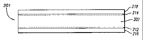
Figure 2A shows a sectional view of an n-type Si substrate with phosphorus
as the n-type dopant source and aluminum as the p-type dopant source;
Figure 2B shows a sectional view of a p-n junction diode with self-doping
contacts formed from the structure of Figure 2A according to an embodiment of
the
to present invention;
Figure 3A shows a sectional view of an n-type Si substrate with phosphorus
as the n-type dopant source and boron as the p-type dopant source;
Figure 3B shows a sectional view of a p-n junction diode with self-doping
contacts formed from the structure of Figure 3A according to an embodiment of
the
is present invention;
Figure 4 shows a cross-sectional view of a silver particle coated with liquid
dopant, where such a coated particle is suitable for incorporation into a
screen-
printing paste;
Figure 5 shows a silver-silicon phase diagram which is utilized in accords nce
2o with the present invention;
Figure 6 shows a current versus voltage plot of a Ag/np+/AI sample structure
after 800 degrees C, two minute heat treatment;
Figure 7 shows a current versus voltage plot of a Ag/ n+np+/AI sample
structure after 900 degrees C, two minute heat treatment;
2s Figure 8 shows a current versus voltage plot of a Ag/n+nn+/Ag resistor
structure obtained with phosphorus dopant on both Ag surfaces, processed at
900
degrees C for two minutes;
Figure 9 shows a current versus voltage plot of a Ag/n+np+/Ag diode
structure obtained with phosphorus dopant on one Ag surface and boron dopant
on
3o the other Ag surface, processed at 900 degrees C for two minutes;
Figure 10 shows a phosphorus and silver depth profile of a sample after
removal of the front silver surface, alloyed at 1000 degrees C for two
minutes;
CA 02392342 2002-05-21
WO 01/41221 PCT/US00/32257
Figure 11 shows a current versus voltage plot of a fully metallized resistor
structure with self-doping contacts formed according to an embodiment of the
present invention; and
Figure 12 shows a current versus voltage plot of a fully metallized diode
s structure with self-doping contacts formed according to an embodiment of the
present invention.
Figure 13 shows a current versus voltage plot, measured under an
illumination level of 100 mW/cm2, of a fully metallized solar cell with self-
doping
contacts formed according to an embodiment of the present invention.
to
is
6
CA 02392342 2002-05-21
WO 01/41221 PCT/US00/32257
DETAILED DESCRIPTION OF PREFERRED EMBODIMENTS
The following description is provided to enable any person skilled in the art
to make and use the invention, and is provided in the context of a particular
application and its requirements. Various modifications to the embodiments
will be
s readily apparent to those skilled in the art, and the generic principles
defined herein
may be applied to other embodiments and applications without departing from
the
spirit and scope of the invention. Thus, the present invention is not intended
to be
limited to the embodiments shown, but is to be accorded the widest scope
consistent with the principles, features and teachings disclosed herein.
io One approach to producing self-doping contacts uses a combination of
materials and processing conditions which produces a self-doping negative
electrode for silicon solar cells, similar in function to the widely-used
aluminum
self-doping positive electrode. Experimental results have shown that a
combination
of antimony as the n-type dopant and silver as the primary contact metal
satisfies
Is the basic requirements for a self-doping negative electrode. Alternatively,
analogous self-doping positive electrodes have been proposed using gallium and
silver. This approach requires that the contact material be applied to silicon
as a n
alloy of silver and a dopant, such as silver-antimony or silver-gallium.
Current
technology for producing small (3 micron) silver particles for incorporation
into a
2o screen-printing paste utilize the precipitation of silver particles from a
solution of
silver nitrate, and is not suitable for producing particles composed of silver
and a
dopant in alloy form. Another approach introduces dopant atoms to the process
separately from a remote source, generally a gas, during the heating process.
An embodiment of the present invention which does not require the
2s application of an alloy of silver and a dopant or a remote doping source is
illustrated
in Figures 1 A and 1 B. Figure 1 A shows a sectional view of a starting
structure
comprising a silicon (Si) substrate 102 contacted by a layer of silver (Ag)
104
which, in turn, is coated with a layer containing a dopant 106. Ag is a widely-
used
contact metal because of its low electrical resistivity and solderability. The
dopant
30 layer 106 may be applied using a commercially-available liquid source.
Alternatively, the Ag layer 104 and dopant layer 106 may be applied by
sputtering,
screen printing or evaporation.
7
CA 02392342 2002-05-21
WO 01/41221 PCT/US00132257
If the temperature of this structure is raised above the Ag-Si eutectic
temperature (> 835°C), Ag can alloy with Si to form a liquid pool
containing Ag, Si,
and the dopant. As shown in Figure 1 B, while cooling to 835°C the Si
re-grows by
liquid phase epitaxy and incorporates dopant atoms into the epitaxial Si layer
112.
s When the temperature drops below 835°C, the liquid pool solidifies
abruptly into a
two-phase eutectic region 118; a Si phase 114 which also contains dopant, and
a
Ag phase 116 which is electrically conductive and contains some dopant as wel
I ,
the two phases being in intimate contact.
A preferred conductive metal for this invention is silver. In addition to its
higt-~
io electrical conductivity, silver has the desirable property that its oxide
is unstable at
temperatures only modestly elevated above room temperature. This means that
the alloying process described will yield a contact with an oxide-free
surface, even if
the alloying is done in air or in oxygen. The oxide-free silver contact is
very wel I
suited for soldering when cells are interconnected to form a module. In
addition,
is the formation of a self-doping negative electrode at a temperature in the
range of
835°C to 1000°C means its formation can be combined with the
creation of a
thermal oxide layer grown on the exposed silicon substrate. This oxide layer
would
serve to passivate the silicon surface, thereby reducing the loss of
photogenerated
electrons and holes by recombination at the surface.
2o This concept can now be applied to create a complete p-n junction diode
from an n-type Si substrate in a single high-temperature step (>
835°C). Figure 2A
shows a sectional view of an n-type Si substrate 202 with an Ag layer 204
coated
with a liquid phosphorus (P) layer 206 as the n-type dopant source and an
aluminum (AI) layer 208 as the p-type dopant source. Figure 2B shows a cross
2s sectional view of the substrate of Figure 2A after high temperature
alloying. AI is
used to form the p+ region 212 as well as ohmic contact to that p+ region,
while Ag
coated with P is used to form the n+ region 214 and ohmic contact to it. The
contact metals are AI-Si eutectic 216 and Ag-Si eutectic 218, respectively.
The
final Ag/n+np+/AI structure 201 constitutes a complete p-n junction diode with
self
3o doping contacts. Note that no separate dopant diffusion step is needed in
this
process. Dopant to create the n+ and p+ regions is supplied either directly by
the AI
or indirectly by the P coating on the Ag via the metal layers.
8
CA 02392342 2002-05-21
WO 01/41221 PCT/US00/32257
A second embodiment of the present invention is illustrated in Figures 3A and
3B. Figure 3A shows a sectional view of an n-type Si starting substrate 302
with a
first Ag layer 304 coated with a liquid P layer 306 as the n-type dopant
source and
a second Ag layer 308 coated with a liquid Boron (B) layer 310 as the p-type
s dopant source. Figure 3B shows a cross sectional view of the substrate of
Figure
3A after high temperature alloying. Analogous to the first embodiment, B is
used to
form the p+ region 312 as well as ohmic contact to that p+ region, while Ag
coated
with P is used to form the n+ region 314 and ohmic contact to it. The final
Ag/n+np+/Ag structure 301 constitutes a complete p-n junction diode with first
io solderable Ag contacts 316 and second solderable contacts 318.
Solderability
follows from the fact that the oxide of Ag is volatile above room temperature,
so that
a clean Ag surface is present after alloying at high temperature.
A third embodiment of the present invention, shown in Figure 4, combines
two existing materials, Ag in particle form and a dopant in liquid form, to
create a
is self-doping, screen printable paste. Rather than coat a planar Ag surface
with
dopant, as illustrated previously, the entire outer surface of an individual
Ag particle
402 is coated with a dopant layer 404. These coated Ag particles 401 can then
be
introduced into a paste formulation with binders, solvents, etc., to make a
screen-printing paste (not shown). Silver pastes, usually with glass frit, are
widely
2o used in the photovoltaic industry. Therefore, a dopant material which can
be
applied as a coating to Ag can generally function as a dopant source in the
alloying
process. This includes a variety of commercially-available liquid dopants such
as
P, antimony (Sb), arsenic (As), indium (In), aluminum (AI) and gallium (Ga). A
coating of elemental Sb, AI, Ga, or In on the Ag particles may also serve as a
2s dopant source. Since it is not uncommon for manufacturers of screen-
printing
pastes to coat Ag particles with a layer of material to prevent agglomeration
of the
small particles, the technology for applying a coating to Ag particles already
exists
for some materials. This embodiment of the invention in which each Ag particle
in
the paste is coated with liquid dopant can be applied to make screen-printing
paste.
3o A silver-silicon phase diagram for this method is shown in Figure 5. The
vertical axis of Figure 5 is temperature in degrees centigrade, while the
horizontal
axis is percentage silver. The horizontal axis has two scales: a lower scale
of
percent silver (by weight) and an upper scale of percent silver (atomic). A
eutectic
point 502 is found at 96.9 % Ag and 3.1 % Si (by weight). Eutectic point 502
lies on
9
CA 02392342 2002-05-21
WO 01/41221 PCT/US00/32257
line 504 which indicates a temperature of 835°C. Also shown are the
melting point
506 of Ag (961.93°C) and the melting point 508 of Si (1414°C).
Curve 510 (which
rises leftward from point 502) indicates that as the temperature is further
increased
above the eutectic, the percent Si, which can be held in a molten mixture of
Si and
s Ag, also increases. Silver is therefore capable of dissolving silicon at
temperatu res
above 835°C, and then allowing the silicon to recrystallize by liquid
phase epitaxy
upon cooling, in analogy with the behavior of aluminum. Unlike aluminum,
however, silver is not a dopant in silicon, so a dopant, some of which will
remain in
the silicon upon epitaxial re-growth, must be added to the silver. From the
phase
to diagram it can be seen that the eutectic material will have two regions
(phases), a
major region which is nearly pure Ag and a minor region which is nearly pure
Si.
The phase diagram of Figure 5 also gives a way of determining the amount of
silicon that a given thickness of silver will dissolve. It thereby provides a
means for
estimating eutectic layer thickness and n+n junction depth for the case where
Ag is
is in contact with an n-type substrate and is coated with an n-type dopant.
The ratio
of thickness of silicon dissolved (ts;) to thickness of silver deposited (tA9)
at an
alloying temperature (T) is given by:
(tsi)/(tA9) _ (Pa9)/(Ps~)*Lws~(T)/(100% - ws;(T))~ (1 )
where pA9 is the density of silver (10.5 g/cm3), ps; is the density of silicon
(2.33 g/cm3), and ws;(T) is the weight percent of silicon at the processing
temperature. With ws;(T = 835°C) of 3.1 % from the phase diagram, the
thickness
ratio is calculated from Equation (1 ) to be 0.144. Thus, the Ag-Si eutectic
layer will
2s be 1.144 times as thick as the Ag layer.
The depth of the n+n junction that would be found beneath the Ag region of the
eutectic layer depends on the temperature at which the alloying was done, as
indicated by Equation (1 ). (The n+ region is the heavily-doped epitaxial
layer 11 2 in
Figure 1B.) For example, at 900°C, ws; is 4.0% (from the left liquidus
branch of the
3o phase diagram because excess Si is available for the limited Ag to
dissolve) and
ts;/tAg is 0.188, while at 1000°C, ws; is 5.8% and ts;/tA9 is 0.278.
The depth of the
junction beneath the Ag region for a contact alloyed at temperature T is then
given
by:
CA 02392342 2002-05-21
WO 01/41221 PCT/US00/32257
Xj(T) = Otgi(T) - ~~tSi~tA9~(T) - ~tSi~tA9~(Teutectic)) * tA9 (2)
Equation (2) shows that xj(T = 900°C) is 0.044 * tA9 and xj(T =
1000°C) is
0.134 * tA9. For example, a 10 ~m thick Ag layer will dissolve 1.88 ~m of Si
at
s 900°C and create a junction depth of 0.44 ~m upon epitaxial re-
growth, while at
1000°C a 10 ~m thick Ag layer will dissolve 2.78 ~.m of Si and create a
junction
depth of 1.34 Vim.
It is noteworthy that semiconductors other than silicon interact with silver
in a
similar way. In particular, the binary phase diagram of germanium with silver
io exhibits a eutectic at 650 C having composition 81 % silver and 19%
germanium by
weight. The melting point of germanium is 937 C. Like silicon, germanium is a
member of Group IV of the periodic table so that elements from Group III and
Group V act as p-type and n-type dopants in germanium, respectively. Germanium
also crystallizes in the diamond cubic structure, like silicon. This means
that the
is concept of a self-doping contact, as described above for silicon and
silver, can be
extended to germanium and to semiconductor alloys of silicon and germanium.
EXPERIMENTAL RESULTS
2o Embodiments of this invention have been tested experimentally with silicon
using both evaporated Ag layers and screen-printed Ag layers, and the key
features of the self-doping alloyed Ag contacts have been demonstrated. Diodes
and resistors were made using evaporated Ag along with liquid P and B dopants.
Electrical measurements, including current-voltage (I-V) curves and spreading
2s resistance profiles, as well as examinations by scanning electron
microscopy
(SEM), scanning Auger microanalysis (SAM), and secondary ion mass
spectroscopy (SIMS) confirmed the creation of a self-doping contact when the
processing temperature exceeded the eutectic temperature. Contact (interface)
resistance and bulk metal resistivity were consistent with an effective ohmic
3o contact. In addition, an experimental Ag paste has been formulated where
the
individual Ag particles have a coating which acts as a source of P dopant.
Optical
microscopy has shown that this paste gives rise to Ag-Si alloying. I-V curves
for
resistors and diodes, type-testing, and measurements of contact resistance and
spreading resistance all show that this paste is self-doping. Solar cell grid
patterns,
11
CA 02392342 2002-05-21
WO 01/41221 PCT/US00/32257
and prototype dendritic web solar cells have also been made using this paste.
Such a paste is desirable as a cost-effective means of implementing self-
doping
contacts in solar cells.
Samples were prepared using dendritic web silicon substrates, 2.5 cm X
s 10.0 cm in area, approximately 120 ~,m thick, and doped n-type (Sb) to
approximately 20 S2-cm. A layer of Ag, 2 - 4 ~m thick, was evaporated on one
side
of the substrate and a layer of AI, 2 - 4 ~m thick, was evaporated on the
opposite
side. A coating of Filmtronics P507 liquid phosphorus dopant from Filmtronics
Semiconductor Process Materials of Butler, PA, was painted onto the Ag surface
in
io most cases and then dried. Heat treatment was done in a Modular Process
Technology (MPT) model 600S rapid thermal processing (RTP) unit at
temperatures ranging from 800°C to 1000°C, typically for 2
minutes in flowing
argon (Ar) gas. With this temperature range, the AI-Si eutectic temperature
(577°
C) was always exceeded, so the AI always gave rise to a p+ layer. However, the
is Ag-Si eutectic temperature (835°C) was exceeded in some cases and
not in others.
In addition, some test structures were processed over the same temperature
range
with no P507 phosphorus dopant layer applied to the Ag surface.
In a first experiment, a starting structure comprising an n-type Si substrate
contacted by a layer of Ag was, in turn, coated with a layer containing a
dopant.
2o The structure was subjected to 900°C, 2 minute, RTP heat treatment,
and then
cooled. Under SEM inspection (without the Ag layer removed), two distinct
regions
on the Ag surface were clearly evident as expected from the phase diagram of
Figure 5 and the schematic of the Ag-Si eutectic layer 118 of Figure 1 B.
Auger
spectroscopy with depth profiling was used to show that darker regions were Si
and
2s lighter regions were Ag. Symmetrical patterns reflected the surface
orientation of
the Si web substrate. Thus, alloying of Ag and Si occurred, as expected, since
the
processing temperature (900°C) exceeded the eutectic temperature
(835°C).
Several small particles (approximately 1 - 2 Vim) of Ag were also present on
the
surface.
3o In a second experiment, a 2.5 cm x10.0 cm P507/Ag/n-Si/AI substrate
structure
was processed at 800° for 2 minutes. After cooling, a 2.0 cm x 2.0 cm
sample was
cut from the structure and electrically tested. The resultant I-V curve 602,
represented in Figure 6, indicated only very high resistance exceeding 1 kS2-
cm2 _
12
CA 02392342 2002-05-21
WO 01/41221 PCT/US00/32257
Such a high resistance is a consequence of the failure of the Ag and Si to
alloy,
since the processing temperature was below the eutectic temperature.
Consequently, there was no liquid region formed and no way for the dopant to
become incorporated into the surface of the Si. This was confirmed by
examining
s the Si surface under SEM inspection after the Ag was removed by etching. The
surface was featureless, indicating no alloying and no self-doping action.
Only a
highly-resistive Ag/np+/AI structure was created.
In a third experiment, a 2.5 cm x10.0 cm P507/Ag/n-Si/Al substrate structure
was processed at 900° for 2 minutes. After cooling, a 2.0 cm x 2.0 cm
sample was
to cut from the structure and electrically tested. The resultant I-V curve
702,
represented in Figure 7, indicated the formation of a self-doping Ag/n+np+IAI
structure, and the creation of a textbook-like Si diode. The low-leakage p+n
junction is an AI alloy junction. The low resistance ohmic contact to the n-
type
substrate follows from the alloying action of Ag, in conjunction with a P
dopant
is source, to create the n+ layer. After the Ag was removed by etching, SEM
inspection revealed that the Si surface exhibited a distinct topography
associated
with the formation of the Ag-Si eutectic. As represented in Figure 1 B, the Si
columns 114 were raised approximately 2 ~m above the floor of the silicon 112
which had been covered with the Ag portions of the eutectic layer 118 prior to
Ag
2o etching. A measurement of the sheet resistance of the front Si n+ surfaces
gave
70 S2/0 for the surface. Other measurements showed that the resistivity of the
Ag-Si eutectic contact metal is 2.0 times as high as the resistivity of the
evaporated
Ag. However, the resistivity of the eutectic metal is still quite low at ~ 6
~S2-cm,
considering the handbook value of resistivity for bulk Ag is 1.6 x.52-cm.
2s In a fourth experiment, a 2.5 cm x10.0 cm P507/Ag/n-Si/AI substrate
structure
was processed at 1000° for 2 minutes. After cooling, a 2.0 cm X 2.0 cm
sample
was cut from the structure and electrically tested. The resultant I-V curve
was
essentially identical to curve 702 represented in Figure 7, and again
indicated the
formation of a self-doping Ag/n+np+/AI structure, and the creation of a
textbook-lil~ce
3o Si diode. A measurement of the sheet resistance of the front Si n+ surfaces
gave
40 S2/0 for the surface. Other measurements showed that the resistivity of the
Ag-Si eutectic contact metal is 2.2 times as high as the resistivity of the
evaporated
13
CA 02392342 2002-05-21
WO 01/41221 PCT/US00/32257
Ag. In both the third and fourth experiments, the structure 201 of Figure 2B
was
therefore realized in practice.
An estimate of the I-V curve that might result if this process were applied to
a
dendritic web silicon solar cell structure can be made by translating the I-V
curve
s 702 of Figure 7 downward along the current axis by 120 mA (typical JS~ value
of
30 mA/cm2). Such an estimate gives V°~ of 0.57 V, Fill Factor (FF) of
0.78, and
efficiency (r1) of 13%. The sharp knee 704 of the diode I-V curve 702 (as also
indicated by the high estimated FF), the high estimated V°~, and the
low reverse
bias leakage current all suggest that Ag is not contaminating the Si substrate
or the
io p-n junction at 900°C or 1000°C. The implication is that high
efficiency solar cells
can be made with this contact system. This was later confirmed when complete
solar cells were fabricated using a self-doping silver paste, as shown in
Figure 13.
Additional information regarding contact resistance was obtained by
evaporating approximately 2 pm Ag on both sides of an n-type web substrate and
Is applying phosphorus liquid dopant to both Ag surfaces for a starting
structure of
P507/Ag/n-Si/Ag/P507. After RTP alloying at 900°C for 2 minutes, the
linear I-V
curve 802 of Figure 8 was obtained, indicating the formation of a resistor
with a
Ag/n+nn+/Ag structure. From the slope of the I-V curve 802, a specific
resistance of
0.12 Sz-cm2 is obtained. This can be attributed entirely to the resistance of
the
2o silicon substrate, indicating a negligible contact resistance associated
with the Ag
metal and Ag/Si interface.
To illustrate the versatility of the Ag-based self-doping contact system,
phosphorus liquid dopant was applied to one Ag surface and a commercial boron
liquid dopant (Boron-A) from Filmtronics was applied to the other Ag surface
to give
2s a starting structure of P507/Ag/n-Si/Ag/Boron-A. After RTP alloying at
900°C for
2 minutes, the rectifying I-V curve 902 of Figure 9 was obtained, indicating
the
formation of a Ag/n+np+/Ag structure in one high-temperature step. In this
case the
p-n junction was formed by alloying Ag with Si in the presence of B dopant,
while
ohmic contacts followed from the creation of the n+ and p+ layers in intimate
contact
30 with the Ag-Si eutectic layer. The structure 301 of Figure 3B was therefore
realized
in practice.
Measurements of I-V curves and sheet resistance indicated P had been
incorporated into the Si to form an n+ layer during alloying, but did not
detect P
14
CA 02392342 2002-05-21
WO 01/41221 PCT/US00/32257
directly. SIMS was employed to determine the composition of the surface layer
for
samples taken in the second, third and fourth experiments after the front Ag
was
removed. Data showed doping of 2 x 10²° P/cm3 to a depth of 0.3 ~m at
900°C, 2 X
102° P/cm3 to a depth of 0.4 ~m at 1000°C, and no appreciable P-
doping at 800°C,
s in good agreement with diode I-V curves. This shows that a necessary
condition
for the formation of a self-doping contact is that Ag alloy with Si, i.e.,
that the
processing temperature exceed the eutectic temperature of 835°C. As
seen in
Figure 10, Ag appeared to be below the detection limit (< 1 x 1 O'S Ag/cm3) at
depths greater than 1 Vim, suggesting that Ag will not contaminate the Si in
the
to alloying process (in agreement with the diode I-V curve 702 of Figure 7).
The S I MS
depth profile 1002 for P and depth profile 1004 for Ag for the sample alloyed
at
1000°C for 2 minutes is shown in Figure 10, where an n+n junction depth
of 0.4 E~.m
is indicated. From Equation (2) this depth implies a starting Ag thickness of
3.0 ~~.m,
which is consistent with the estimated thickness of evaporated Ag of 2 - 4 pm.
The
is gradual reduction in measured P and Ag concentrations from 0.4 ~m to 1.0 ~m
in
Figure 10 may be associated with the Si columns in the eutectic layer which
are
presumed to contain P and Ag. The overall P concentrations and junction depths
obtained by SIMS are in reasonable agreement with those obtained by spreading
resistance measurements.
2o Some Ag/n-Si/AI samples were prepared with no dopant coating on the Ag
layers. After processing under the same conditions described previously
(temperatures up to 1000°C), I-V curves showed extremely high series
resistance.
This demonstrates that self-doping action does not occur because of the Ag
itself,
but only if a dopant coating is applied to the Ag surface. These experiments
2s suggest that conditions for achieving a self-doping Ag contact to Si are:
1. Coating the Ag surface with a dopant source;
2. Using a processing temperature which exceeds the Ag-Si eutectic
temperature so that alloying of Ag with Si occurs.
3o The self-doping alloyed Ag contact system has also been implemented in a
screen-printing paste. DuPont Electronic Materials, Research Triangle Park,
NC,
has formulated an experimental paste in response to a request and
specification
CA 02392342 2002-05-21
WO 01/41221 PCT/L1S00/32257
from EBARA Solar. This paste is designated by DuPont as E89372-146A, and
contains Ag particles~which are coated with a layer which contains P.
The ability of the 146A paste to create a self-doping contact was demonstrated
by converting the surface of a p-type dendritic web silicon substrate to n-
type. A
s p-n junction diode (sample 146A-1000p) was fabricated with a low-resistivity
p-type
web (0.36 S2-cm) serving as the starting substrate. A back ohmic contact was
made by alloying Ferro FX-53-048 AI paste to make a pp+ structure. DuPont 146A
paste was then printed over nearly the entire front of the blank (2.5 cm x
10.0 cm)
and dried (200°C, 10 minutes, Glo-Quartz belt furnace). Binder burnout
and Ag
io alloying were done in the MPT RTP, with alloying at 1000°C for 2
minutes in Ar. A
2 cm x 2 cm piece was cut from the blank. The measured I-V curve was rectifyi
ng,
with a shunt resistance of 1.6 kS2-cm2, a soft turn-on voltage of ~ 0.5 V and
series
resistance in the forward direction < 0.94 S2-cm2. The creation of a diode on
a
p-type substrate indicates an n+ layer was formed beneath the 146A metal, as
is desired, to give a Ag/n+pp+/AI structure. This was confirmed by removing
the Ag
metal in HN03. The underlying Si was found to be strongly n-type by a hot
probe
type tester, and the sheet resistance was measured in the range 4 - 28 S2/~.
Tti us,
the front Si structure was confirmed to be n+p, with 146A paste supplying the
n-type
dopant. For comparison, another p-type web blank was printed with DuPont
2o E89372-119A Ag paste, which is similar to the 146A paste but without the
phosphorus-containing coating, and alloyed as above. Upon stripping the Ag
from
the front, the underlying Si tested p-type, as expected, since the 119A has no
source of P. The supposed structure then is Ag/pp+/AI for the 119A paste which
is
not self-doping. This confirmed that the structure 401 of Figure 4 was
realized i n
2s practice with the 146A paste.
Additional work with the 146A paste further confirmed its ability to serve as
a
self-doping contact material. A fully metallized Ag/n+nn+/Ag resistor and a
Ag/n+np+IAI diode were fabricated using n-type web silicon cell blanks (2.5 cm
x
10.0 cm) in one high temperature step (900°C, 2 minutes, 1 slpm Ar) in
the MPT
3o RTP. The source of AI for the diode was the commercial Ferro FX-53-048 AI
pa ste.
Alloying of Ag with Si was uniform, with only small balls of metal appearing
on tt-~e
surface and no unalloyed areas. Good ohmic contact was obtained for the
resistor
(0.12 S2-cm2, including 0.07 S2-cm2 resistance of bulk Si) as shown in Figure
11.
16
CA 02392342 2002-05-21
WO 01/41221 PCT/US00/32257
The linear I-V curve 1102 demonstrates ohmic contact to the 7 S2-cm n-type
dendritic web Si substrate. Total resistance of 0.12 S2-cm2 includes 0.07 S2-
cm2
associated with the Si (nominal thickness of 100 Vim), leaving an estimated
net
Ag/n+ contact resistance of 25 mS2-cm2.
s Turning to Figure 12, the Ag/n+np+/AI diode was also shown to have very low
leakage current as indicated by its high shunt resistance. Dendritic web Si
substrate was nominally 100 pm thick and had a resistivity of 7 S2-cm. Note
the low
leakage current (as represented by curve 1202) and the sharp knee 1204 of the
curve.
io The ability to print and alloy patterns using the 146A Ag paste was also
demonstrated. A solar cell grid pattern with Ag lines having a nominal 100 ~m
width was printed and alloyed, along with a contact resistance test pattern
utilizi ng
the current transfer length method (TLM) comprising a series of bars 1 mm wide
and 25 mm long. The contact resistance test pattern was printed on 6.8 S2-cm
is n-web (no diffused layer) and fired at 950°C in the MPT RTP. This
gave uniform,
adherent contacts which showed evidence of Ag-Si alloying (triangles
reflecting the
web silicon surface, apparent two-phase region at the surface), and measured
contact resistance of 2.8 mS2-cm2 for the 146A paste. It was further
determined
that phosphorus from the Ag was doping the Si beneath the metal by stripping
the
2o metal and probing the Si surface using the spreading resistance technique.
Measured spreading resistance decreased by a factor of 1000 when the probes
passed from the region beside the Ag bar (6.8 S2-cm) to the region originally
beneath the Ag bar. This implies a surface concentration of 8 x 10'$ PIcm3
supplied by the 146A paste. Simultaneous type testing also confirmed that both
the
2s substrate and the region beneath the metal were n-type.
The bulk resistivity of the screen-printed and alloyed 146A paste has been
measured to be 5 ~SZ-cm, which is sufficiently low and not much greater than
th a
1.6 X52-cm value for pure Ag. Tabs used for interconnecting cells in a module
h ave
also been soldered to the alloyed 146A surface. Thus, electrical conductivity
an d
3o solderability of the 146A paste have been demonstrated.
The DuPont 146A fritless, self-doping paste was used to form the negative
contact to PhosTop web solar cells with an Ag/n+pp+/AI structure, and having
n+
sheet resistances of 35 S2/~ and 70 S2J~ (Lot PhosTop-46). Alloying of 146A Ag
17
CA 02392342 2002-05-21
WO 01/41221 PCT/US00/32257
was done in the MPT RTP at 900°C for 4 minutes. Results are tabulated
in Table 1
below for cells fabricated without an anti-reflective (AR) coating. Commercial
Ferro 3347 fritted Ag paste, fired in a belt furnace at 730°C, is
included for
comparison. In all cases AI alloying in a belt furnace at 850°C
followed the P
diffusion and preceded the Ag alloying or firing. At 35 S2/0, where the Si
surface is
pre-doped liberally with P, cell efficiency for the self-doping 146A Ag is
comparable
to, but no better than, that for the 3347 Ag. However, at 70 S2/0 the 146A
gives
considerably better efficiency than does the 3347. The reason for this is that
the
series resistance is quite high (approximately 20 S2-cm2) for 3347 because of
an
Io insufficient concentration of P at the Si surface, but is at an acceptable
level for
146A which supplies its own P. These results show that the 146A Ag paste
enables the use of a more lightly-doped P layer, which is expected to lead to
higher
efficiency cells when the Si surface is properly passivated. It is also
expected that
an alloying process which can be executed in a belt furnace rather than an RTP
is can be developed for 146A to achieve higher throughput and lower cost.
TABLE 1
Ag PasteRsheet# CellsJS~ (no V Fill FactorEfficiency
AR)
(mA/cm2) (V) (FF) (%)
Ferro 35 30 20.2 0.578 0.0060.758 0.0168.86
0.4 0.35
3347 (20.7 (0.583 best)(0.779 best)(9.24
best) best)
DuPont 35 10 18.6 0.557 0.0170.724 0.0487.49
1.9 1.01
146A (20.5 (0.587 best)(0.767 best)(9.04
best) best)
Ferro 70 19 13.4 0.527 0.0090.417 0.0913.02
1.8 0.99
3347 (16.4 (0.554 best)(0.596 best)(4.75
best) best)
DuPont 70 10 19.0 0.557 0.0050.728 0.0117.69
0.3 0.23
146A (19.5 (0.563 best)(0.743 best)(8.09
best) best)
Additional work was done in which self-doping Ag pastes were alloyed after P
diffusion, but before AI alloying. DuPont 146A fritless Ag paste as well as
DuPont 151 B fritted Ag paste were used. Ag particles in the 151 B paste were
identical to those in the 146A paste in that a phosphorus-containing coating
had
2s been applied to them, but glass frit had been added to the coated paste so
that
151 B was a fritted version of the 146A Ag paste. The best results obtained
when
18
CA 02392342 2002-05-21
WO 01/41221 PCT/US00/32257
Ag alloying (900°C for 4 minutes in the MPT RTP for 146A or
940°C for
approximately 1 minute in a belt furnace for 151 B) preceded AI alloying
(800°C for
approximately 3 minutes in a belt furnace in both cases) are summarized in the
Table 2 below.
s TABLE 2
Ag Paste Rsheet PhosTop J5~(no V~ Fill FactorEfficiency
(S2/p) Lot # AR) (V) (FF) (%)
(mA/cmz)
DuPont 146A57 56 20.2 0.578 0.752 8.76
DuPont 146A69 56 20.2 0.584 0.733 8.65
DuPont 151 78 58 18.6 0.577 0.753 8.09
B
These data show that good fill factors and other solar cell parameters can be
io obtained when the self-doping Ag pastes are applied to a Si surface doped
lightly
(approximately 70 SZ/0) with P. An estimate of the efficiency expected if the
three
cells in the above table had an AR coating can be obtained by multiplying the
observed efficiency (no AR) by 1.45. This gives 12.7%, 12.5%, and 11.7%,
respectively, and confirms the expectations of Figure 7 that screen-printed
Is self-doping Ag contacts can be used for solar cells. Furthermore, the fact
that the
151 B fritted Ag paste can be alloyed in a belt furnace shows that such a
paste is
compatible with a practical, high-throughput process for forming contacts. The
fabrication of cells made with the 151B Ag paste was accomplished by
screen-printing (P, Ag, and AI) along with belt furnace P diffusion
(870°C), Ag
2o alloying (940°C) and AI alloying (800°C).
Finally, dendritic web silicon solar cells having self-doping silver contacts
were
fabricated, complete with an anti-reflective (AR) coating. The AR coating was
silicon nitride (nominal 86 nm thickness and 1.98 index of refraction),
deposited by
plasma-enhanced chemical vapor deposition (PECVD) onto the front n+ silicon
zs surface. This was followed by screen-printing and alloying aluminum to form
the
p+n junction and back contact. The structure to which DuPont experimental 151
A
or 151 B fritted self-doping Ag paste was applied was: SiNx/n+pp+/AI. By
virtue of
the glass frit, these pastes were able to penetrate through the insulating
silicon
nitride layer to make ohmic contact to n+ layers having sheet resistances up
to
30 100 S2/~. This high-throughput process was carried out in a radiantly
heated belt
19
CA 02392342 2002-05-21
WO 01/41221 PCT/US00/32257
furnace at 940 C for 1 minute. The illuminated I-V curve 1302 for such a cell
(Lot
PhosTop-69, cell 111, 151A paste) is given in Figure 13. Cell area is 25 cm2,
and
doping of the n+ layer is very light at 100 521. Cell efficiency is 13.4%,
with JS~ of
30.0 mA/cm2, V°~ of 0.593 V, and FF of 0.752. In spite of the very
light n+ doping,
s the series resistance for this cell was determined to be 0.70 S2-cm2, well
within the 1
S2-cm2 limit desired. Attempts to use commercial Ferro 3347 Ag paste failed
for n+
sheet resistances above 45 S2/~ because of excessive series resistance.
The ability of screen-printed 151A and 151 B Ag pastes to penetrate the
silicon nitride and make ohmic contact to a lightly-doped n+ layer using a
high-
io throughput belt furnace process demonstrates a commercially-viable material
and
process. Furthermore, measurements of contact resistance (current transfer
length
method) of 151A and 151 B contacts through PECVD silicon nitride AR coatings
to
60 S2/0 n+ layers gave 3 mSZ-cm2, equivalent to a series resistance of just
0.03 Sz-
cm2. Commercial Ferro 3347 Ag gave 500 mS2-cm2 contact resistance under the
is same conditions, equivalent to a series resistance of 5 S2-cm2,
considerably above
the 1 S2-cm2 limit. Measured bulk resistivity of-the 151A and 151 B Ag contact
material was quite low at 2 x,52-cm, and the contacts were readily solderable.
Considering the test results in total for the DuPont E89372-146A fritless
paste and the DuPont E89372- 151A and 151 B fritted pastes, it is clear that a
2o self-doping Ag paste has been realized for making ohmic contact to n-type
silicon.
Such pastes, or a successors to them, are expected to provide a practical,
cost-effective material for making self-doping negative electrodes to solar
cells and
other Si devices by alloying the dopant-coated Ag with Si. There is no obvious
reason why silver pastes incorporating coatings of a p-type dopant could not
be
2s made as well. In theory, the process should also be applicable to other
substrates
such as germanium and silicon-germanium alloys.
The foregoing description of the preferred embodiments of the present
invention is by way of example only, and other variations and modifications of
tl-~e
above-described embodiments and methods are possible in light of the foregoing
3o teaching. The embodiments described herein are not intended to be
exhaustive or
limiting. The present invention is limited only by the following claims.