Note : Les descriptions sont présentées dans la langue officielle dans laquelle elles ont été soumises.
CA 02396105 2002-07-02
1
CIRCUIT ARRANGEMENT COMPRISING A CHAIN OF CAPACITORS
The invention is directed to a circuit arrangement having a plurality of
capacitors connected in series.
Double layer capacitors -- often also called super capacitors or ultra
capacitors
or ultracaps -- enable a new kind of electrochemical energy storage. They lie
between
large aluminum electrolytic capacitors and smaller accumulators in view of the
energy
density and the access time to the energy content. The energy storage in
accumulators
ensues with the assistance of reversible chemical reactions. Capacitors, in
contrast,
exploit the polarization of a dielectric in the electrical field for energy
storage. In
contrast, double layer capacitors have no dielectric. They store the
electrical energy
by charge displacement at the boundary surface between an electrode and an
electrolyte.
The underlying effect is also referred to as Helmholtz effect. This effect
occurs when a voltage is applied between two carbon electrodes immersed into
an
electrolyte. A continuous current thereby only flows when the voltage applied
to the
carbon electrodes exceeds a certain decomposition voltage. At the same time, a
development of gas occurs as a result of a chemical reaction at the surface of
the
carbon electrodes. When, however, the voltage applied to the carbon electrodes
remain [sic] below this decomposition voltage, the carbon electrodes behave
like the
electrodes of a capacitor. Upon application of the voltage, ions from the
electrolyte
deposit at the boundary surface to the carbon electrode, and the carbon
electrodes
correspondingly charge positively or negatively. The energy to be stored is
thereby
dependent on the available surface of the carbon electrode, on the size of the
ions and
on the height of the decomposition voltage.
By employing carbon electrodes composed of activated carbon and electrolyte
having a decomposition voltage of 3 Volts, capacitors having an extremely high
energy density (2Wh/kg) have been successfully developed. Although the power
output of these capacitors is higher than the power output of accumulators, it
is clearly
lower than the power output of traditional capacitors. As a result of various
measure
CA 02396105 2002-07-02
2
[sic], however, the voltage multipliers in the carbon electrodes were capable
of being
clearly lowered and a high power density of above 1000 W/kg was able to be
achieved.
The allowable operating voltage of double layer capacitors, however, remains
limited to a few Volts. Since the operating voltage are [sic] significantly
higher in
most applications, a plurality of double layer capacitors must generally be
connected
in series to form a module. Due to different values of the individual
capacitors as well
as due to different self discharge behavior, however, the total voltage that
is applied is
not uniformly divided onto the individual double layer capacitors. As a result
thereof,
over-voltages that lead to the destruction of the double layer capacitor can
occur at
individual double layer capacitors.
The invention is therefore based on the object of creating a circuit
arrangement
with a plurality of capacitors connected in series wherein the occurrence of
over-
voltages is suppressed in an effective way.
This object is achieved in that the voltages at the capacitors are set by
impedances connected parallel to the capacitors, whereby the sizes of the
impedances
are controlled with the assistance of control means dependent on the voltages
at the
capacitors.
The circuit arrangement of the invention comprises impedances connected
parallel to the capacitors. Since the size of these impedances is variable,
the over-
voltages adjacent at the capacitors can be effectively suppressed by lowering
the value
of the impedance. It is thereby especially advantageous that the impedances
adapt to
the respective operating condition of the circuit arrangement.
A preferred embodiment of the invention involves a chain of double layer
capacitors to which a respective control means is allocated. Module that can
be joined
to one another in an arbitrary number can be formed of the double layer
capacitor and
the allocated control means. The voltage adjacent at the double layer
capacitor is
thereby limited to allowable values in an effective way, so that no harmful
over-
voltages occur at the individual double layer capacitor.
CA 02396105 2002-07-02
3
In another preferred embodiment of the invention, the control means
comprises a two-point regulation that switches the impedances back and forth
between
two prescribed values. Expediently, the two-point regulation is accomplished
with the
assistance of a threshold switch that lowers the value of the impedance given
voltages
at the double layer capacitor above a prescribed threshold voltage. Such a
circuit
arrangement can be constructed with simple means and is nonetheless suited for
attenuating over-voltages that occur at the double layer capacitors.
An exemplary embodiment of the invention is explained in detail below on the
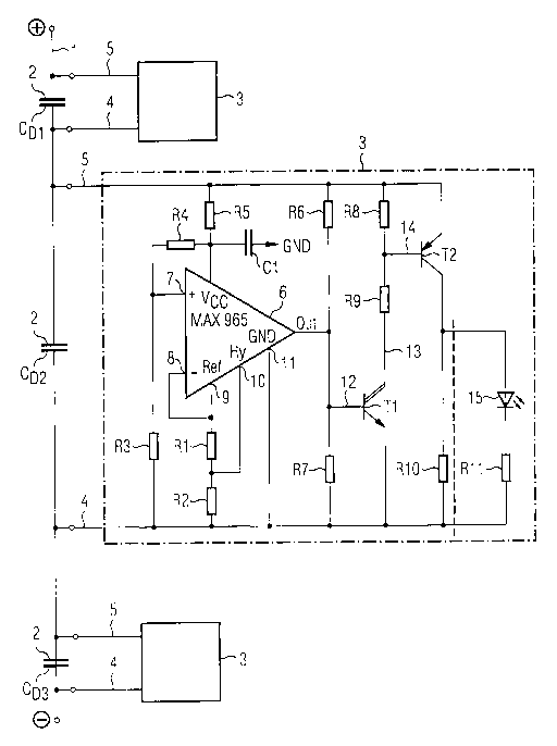
basis of the attached drawing. Shown are:
Figure 1 a circuit diagram of a circuit arrangement according to the
invention.
The circuit arrangement shown in Figure 1 comprises a chain 1 of double layer
capacitors 2 that axe also referenced CD1 through CDn in Figure 1. Modules 3
are
connected parallel to the double layer capacitors 2, the middle module thereof
being
shown in detail in Figure 1.
The module 3 is connected to the chain 1 via a ground line 4 and a voltage
line
5. In this context, the term "ground line" is not intended to mean that the
ground line
4 lies at a defined potential. On the contrary, the potential of the ground
line 4 can
float freely dependent on the voltage applied to the double layer capacitor
CD2. The
term "ground line" is merely intended to express that the ground line 4 has
the
function of a ground within the module 3. The same is true of the voltage line
5.
The central part of the module 3 is the threshold switch 6. Given the
exemplary embodiment shown in Figure 1, this is a matter of a threshold switch
having the designation MAX965 of the Maxim company. The threshold switch 6 is
connected to the voltage line 5 via a low-pass filter formed of a resistor RS
and a
capacitor C1. The low-pass filter formed by the resistor RS and the capacitor
C1
serves for the stabilization of the voltage supply of the threshold switch 6.
The low-
pass filter is followed by a voltage divider composed of the resistors R4 and
R3 via
which the voltage dropping off at the double layer capacitor CDZ is applied to
a non-
inverting input 7 of the threshold switch 6. An inverting input 8 of the
threshold
switch 6 is charged with a voltage from the reference output 9 of the
threshold switch
CA 02396105 2002-07-02
4
6. The reference output 9 also supplies a voltage divider composed of the
resistors Rl
and R2 at which a voltage for a hysteresis input 10 is taken. The hysteresis
of the
threshold switch 6 can be set by means of the voltage adjacent at the
hysteresis input
10. Finally, the threshold switch 6 also has a ground input 11 that is
connected to the
ground line 4.
When the voltage at the non-inverting input 7 exceeds the voltage at the
inverting input 8, an output 12 of the threshold switch 6 becomes low-
impedance and
acts as a current sink. Conversely, the output 12 of the threshold switch 6
becomes
high-impedance when the voltage at the non-inverting input 7 falls below the
voltage
at the inverting input 8.
A pull-up resistor R6 us provided in order to use the switching behavior of
the
threshold switch 6 for generating a voltage signal. As a result thereof, a
voltage
essentially corresponding to the voltage on the voltage line 5 is adjacent at
a following
Darlington circuit 1 [sic] of NPN transistors when the threshold switch 6 is
high-
impedance. Conversely, a voltage corresponding to the voltage on the ground
line 4
lies at the input 12 of the Darlington circuit Tl [sic] when the output 11 of
the
threshold switch 6 is low-impedance.
However, the output 11 of the threshold switch 6 can also become high-
impedance even if it were basically to be switched low-impedance due to the
voltages
pending at the non-inverting input 7 and inverting input 8. This is the case
when the
operating voltage of the threshold switch 6, i.e. the voltage between ground
line 4 and
voltage line 5, falls below an allowable, lower limit value. In this case, the
resistor R7
is provided between the input 12 of the Darlington circuit D 1 [sic] and the
ground line
4. in this case, the input 12 of the Darlington circuit T1 is pulled onto the
potential of
the ground line 4 and a drive of the Darlington circuit T1 is prevented.
A collector terminal 13 of the Darlington circuit T 1 is connected to the base
of
a PNP transistor T2 via a voltage divider composed of a resistor R8 and a
resistor R9.
Accordingly, the transistor T2 opens when the Darlington circuit Tl is through-
connected. Finally, a low-impedance elimination resistor R10 is enabled by the
CA 02396105 2002-07-02
opening of the transistor T2, the voltage adjacent at the double layer
capacitor CDZ
being thereby dismantled.
When the voltage at the double layer capacitor CDZ exceeds the pre-set value,
the module 3 assumes a value of impedance that essentially corresponds to
equal [sic]
the ohmic impedance of the elimination resistor R10.
When, in contrast, the voltage at the double layer capacitor CDZ lies below
the
pre-set value, the module 3 exhibits an impedance with an ohmic resistance
that is
defined above all by the resistors R3 through R7.
In order to indicate the occurrence of an over-voltage at the double layer
capacitor Cp2, a light-emitting diode 15 can be present parallel to the
elimination
resistor R10. Finally, a drop resistor R11 is provided for limiting the
current across
the light-emitting diode 15.
The voltage occurnng at the at the [sic] double layer capacitors 2 is
effectively
limited by the modules 3. One therefore need not fear that over-voltages that
lie
above the allowable limit value can occur at the double layer capacitors. As a
result
thereof, it is possible to construct chains that comprises an overall nominal
voltage of
several 100 V.