Note : Les descriptions sont présentées dans la langue officielle dans laquelle elles ont été soumises.
CA 02397461 2002-07-12
WO 01/52287 PCT/SE01/00064
1
A capacitive element and.electric devices c:omprisi_ng such
an e~_ement
FIELD OF THE INVENTION AND PRIOR ART
The present invention relates to a capacitive object according to
the preamble of claim 1 and a method for production thereof.
The invention also relates to a capacitor and a bank of capaci-
tors. Furthermore, the invention relates to an electric device
having capacitive as well as inductive properties, and a filter for
filtering harmonics in a high voltage network. The invention also
relates to the use of a capacitor and the electric device.
The capacitor and the bank of the capacitors according to the
invention are particularly intended for use in connection with a
network for transmission and distribution of electric power, and
in particular for high voltage applications but also for low volt-
age and medium voltage applications. High voltage here refers
to voltages being higher than 1 kV, preferably higher than 10 kV.
When producing capacitors, it is previously known to let a ca-
pacitor comprise a capacitive object comprising two dielectric
films, each of which in its turn being provided with an electrically
conductive layer on one of its sides. The electrically conductive
layers have interruptions extending in their longitudinal as well
as in their latitudinal direction. The electrically conductive layers
will consequently have a plurality of rectangular, electrically
conductive elements, each of which being electrically insulated
from adjacent electrically conductive elements. Furthermore, the
electrically conductive layers are arranged in such a way in rela-
CA 02397461 2002-07-12
WO 01/52287 PCT/SE01/00064
2
tion to each other that an electrically conductive element in one
of the electrically conductive layers overlaps two electrically
conductive elements in the longitudinal direction of the dielectric
film and two electrically conductive elements in the latitudinal di-
rection of the dielectric film in the other electrically conductive
layer. In this way, a network of capacitor elements is formed,
which capacitive elements are mutually connected in series and
in parallel. The advantage of such an arrangement of a network
of capacitor elements, in comparison with a capacitor which only
has two continuous, electrically conductive layers separated by
a dielectric film, is that a breakthrough in the dielectric film only
results in that a single capacitor element will be put out of op-
eration. The area of the electrically conductive layers being dis-
connected due to the breakthrough is thereby limited to the size
of the electrically conductive element of the capacitor element.
The size of the area of the electrically conductive layers being
disconnected due to the breakthrough will thereby be very small
in comparison with the case for a capacitor having continuous
electrically conductive layers.
Conventional capacitors comprising two dielectric films provided
with layers of electrically conductive elements on one of the
sides of the respective film, are arranged rolled up so as to form
a roll built up in layers. In the radial direction of the roll, every
second layer is therefor of electrically conductive elements and
every second layer of dielectric film.
A dielectric film is provided with a layer of electrically conduc-
tive elements by being covered, normally by steaming, with a
thin layer of metal, such as aluminium or zinc. Said dielectricum
preferably consists of polypropylene.
In a capacitor arranged in the form of a roll and having two
rolled up dielectric films, each of which being provided with said
layer of electrically conductive elements, the layers of electri-
cally conductive elements will form several turns in the roll. The
CA 02397461 2002-07-12
WO 01/52287 PCT/SE01/00064
3
turns increase in circumference with increasing radius. The
electrically conductive elements in the two layers will therefor be
displaced to a different extent in relation to each other in the cir-
cumference direction. This implies, in its turn, that the capacitor
elements formed by the electrically conductive elements will
have different capacitances. A capacitor roll formed in this way
and being put under voltage will therefor have a non-uniform
voltage distribution over the capacitor elements.
The above mentioned capacitors are today used in connection
with networks for transmission and distribution of electric power.
Many electric components, such as for instance transformers
and electric motors, consume reactive power. The generators in
the power stations can deliver such reactive power, but since
the reactive power burdens lines and cables, it is advantageous
to generate the reactive power as close as possible to the load.
Capacitors have a phase angle close to 90° and therefor gener-
ate reactive power. By connecting capacitors close to the com-
ponents that consume reactive power, the desired reactive
power can be generated there. Lines and cables can thereby be
fully used for transmission of active power. The consumption of
reactive power of the load can vary, and it is desirable to always
generate an amount of reactive power corresponding to the con-
sumption. For this purpose, several capacitors are connected in
series and/or in parallel in a so-called bank of capacitors. A re-
quired number of capacitors can be connected so as to corre-
spond to the consumed reactive power. To compensate for con-
sumed power by using capacitors in the above mentioned way is
called power correcting. A bank of capacitors in the form of a
so-called shunt bank is for this purpose arranged closed to the
components that consume reactive power. Such a shunt bank
consists of several capacitor units connected together. The
separate capacitor unit comprises, in its turn, several capaci-
tors. The construction of such a conventional capacitor unit is
explained below. A shunt bank normally comprises a number of
CA 02397461 2002-07-12
WO 01/52287 PCT/SE01/00064
4
chains of several series connected capacitor units. The number
of chains is determined by the number of phases, which nor-
mally is three. The first one of the capacitor units in a chain is
connected to a line for transmission of power to the consuming
component. The line for transmission of electric power is ar-
ranged at a distance from the ground, which distance depends
on the voltage of the line. The capacitor units are connected in
series from the first capacitor unit, which ~is connected to the
line, and downwards. A second capacitor arranged at an end of
the chain of series connected capacitor units opposite the first
capacitor unit is connected to ground. The number of capacitor
units and the construction of these is determined in such a way
that the voltage over the series connected capacitor units corre-
sponds to the voltage in the line. Several capacitor units are se-
ries connected and arranged on platforms on different levels in
altitude at a stand. A number of pin insulators are furthermore
arranged between adjacent platforms. Consequently, such a
bank of capacitor comprises several different components and
requires a relatively large amount of material. Furthermore, a
relatively robust construction is required for the stand to endure
external influence in the form of wind, earthquake etc. It is
therefor laborious to build such a bank of capacitors. This
problem is particularly noticeable when the bank of capacitor
consists of a large number of capacitor units. Furthermore, the
bank of capacitors occupies a relatively large area of land.
Long lines for alternating voltage are inductive and consume re-
active power. Banks of capacitors for so-called series compen-
sation are therefor arranged at mutual distances along such a
line, for generation of the required reactive power. Several ca-
pacitor units are connected in series for compensating the in-
ductive voltage drop. In a bank of capacitors for series compen-
sation, the series connection of the capacitor units normally, in
contrast to a shunt back, only takes up a part of the voltage in
the line. The chains of series connected capacitor units included
CA 02397461 2002-07-12
WO 01/52287 PCT/SE01/00064
in the capacitor bank for series compensation are furthermore
arranged in series with the line to be compensated.
A conventional bank of capacitors comprises several capacitor
5 units. Such a capacitor unit, in its turn, comprises several ca-
pacitors in the form of capacitor rolls. The capacitor rolls are flat
and piled near each other so as to form a pile of for instance 1
m. A very large number of dielectric films with intermediate
metal layers will be arranged in parallel in the vertical direction
of the pile. When a voltage applied over the pile increases, the
pile will be somewhat compressed in vertical direction due to
Coulomb-forces, which act between the metal layers. When the
voltage is lowered, the pile will expand somewhat in the vertical
direction for the same reason. The pile has a certain mechanic
resonance frequency, or natural frequency, which is relatively
low. A strong noise will arise if the frequencies of the current
are close to the mechanic resonance frequency of the pile. Such
a frequency is constituted by the network frequency, which is
defined by the fundamental tone of the current and normally is
50 Hz. Noise can also be caused by overtones of the current.
When producing a capacitor unit, several capacitor rolls, fuses
and discharge resistors are arranged in a container, which
thereafter is being filled with impregnating liquid. Means are
being arranged for connection of the capacitor unit to further
capacitor units. Several capacitor units formed in this way are
subsequently connected so as to form part of a bank of capaci
tors. The assembly of a capacitor unit takes place step by step,
i.e. component after component is being assembled, which is
time consuming and economically disadvantageous.
As mentioned above, the present invention also relates to an
electric device having capacitive as well as inductive properties.
The electric device is particularly intended for use in high volt-
age applications, but can also be used for low and medium volt-
age applications. High voltage here refers to voltages being
CA 02397461 2002-07-12
WO 01/52287 PCT/SE01/00064
6
higher than 1 kV, preferably higher than 10 kV. The electric de-
vice is particularly intended for use in connection with a network
for transmission and distribution of electric power and then in
particular as a filter for the purpose of filtering harmonics.
Henceforth, the inventional electric device having capacitive as
well as inductive properties will be explained when constituting a
filter for filtering harmonics in a network for high voltage. This
field of application is only discussed in exemplifying purpose
and not in any way in a limiting purpose.
Different apparatus arranged in industrial plants, such as static
frequency changers and soft starters, comprise thyristors and
influence or distort the voltage curve in one way or another. This
type of apparatus give an effective use of electric energy, but
they generate disturbances in the form of harmonics on the net-
work. All electric apparatus intended for use in alternating cur-
rent networks are dimensioned for a voltage having a curve
shape in the form of a clean and smooth sine curve. In a net-
work having apparatus which generate harmonics, it is however
more common that the voltage has a distorted curve shape,
where the sine shape is distorted. This distortion is an aggrega-
tion of harmonics. Harmonics are disturbances consisting of
voltage and current having a higher frequency than the funda-
mental frequency, the fundamental tone, of the network. The
harmonics have frequencies which are multiples of the fre-
quency of the fundamental tone. Harmonics are not desired and
can for instance disturb telecommunication as well as computer
and electronic controls.
According to previous technique, a harmonic filter in power ap-
plications consists of a capacitor connected in series with a coil,
a reactor, where the included components are dimensioned so
as to create a series resonant circuit for a given frequency. By
means of such a filter, a harmonic can be filtered away. A so-
CA 02397461 2002-07-12
WO 01/52287 PCT/SE01/00064
7
called tuning frequency for the filter is determined for the filter
by means of the formula (1 ) below, where ~n is the tuning fre
quency, C is the capacitance of the capacitor and L is the in
ductance of the coil. The capacitance of the capacitor depends
on the need of reactive power.
~LC (1)
In order to achieve a filter, a capacitor is arranged in series with
a coil, the capacitor and the coil are produced separately and
are connected to each other via a conduit. The connection of the
capacitor and the coil can either be done before they are trans-
ported to the place where the filter is intended to be arranged,
or be performed at this place.
A conventional capacitor comprises, as mentioned above, a lay-
ered structure formed of two layers of electrically conductive
material rolled up around an axle, which layers are mutually
separated by electrically insulating material. The capacitor is
also provided with means for voltage connection at the ends of
the roll. Each of these means is electrically connected to one of
the electrically conductive layers.
A conventional coil comprises an electric conductor arranged in
several loops, for instance in spiral-shape. When the coil is
traversed by an electric current, a magnetic field is generated,
which is directed through the coil in the longitudinal direction of
the coil.
SUMMARY OF THE INVENTION
A first object of the invention is to develop the capacitive object
indicated in the preamble of the subsequent claim 1 further, in
such a way that it, while maintaining the basic functional fea-
tures of such a capacitive object, obtains a construction that
CA 02397461 2002-07-12
WO 01/52287 PCT/SE01/00064
8
creates the prerequisite of a capacitor production being more
rational than the one used according to known technique.
The first object of the invention is achieved in that the capacitive
object is formed in the way defined in the characterising part of
claim 1. Since the capacitive object is formed as a cable-shaped
conductor having a protective sheath surrounding the elongated
layered structure, very long capacitive objects can be produced
in a manner that is simple from a production technical point of
view, and these capacitive objects can for the production of the
capacitors be used in the lengthes obtained by the method of
production or a separately produced capacitive object can be cut
in several parts, which are one by one used for the formation of
capacitors.
In an advantageous embodiment, the inventional capacitive ob-
ject can be produced in very large lengthes. In case the ca-
pacitive object is designed with such a flexibility that it is wind-
able into roll-shape, the capacitive object can in connection with
the production or at any desired moment thereafter be brought
into the shape of a roll for favourable storage and transport. At
subsequent capacitor production by means of the capacitive
object, required lengthes of the capacitive object are unrolled
from this roll and the capacitive object is cut into parts having
required lengthes.
The invention entails that one single capacitor produced from
such a capacitive object to a long and narrow configuration can
replace arrangements, normally used according to previous
technique, comprising several capacitors connected together so
as to form a capacitor unit. This entails many constructional ad-
vantages. Due to the long and narrow configuration, the total
thickness of the network of the capacitor elements formed by the
layers in the layered structure, will be smaller for a specific ca-
pacitance. When used in a bank of capacitors, a considerably
lower sound level will arise as compared to the sound level
arising when using conventional capacitor units.
CA 02397461 2002-07-12
WO 01/52287 PCT/SE01/00064
9
According to a preferred embodiment of the invention, each of
the electrode forming layers of electrically conductive material
comprises several electrically conductive, electrode forming
elements, and the electrically conductive elements in at least
one of these layers are arranged so as to be displaced in the
longitudinal direction of the capacitive object in relation to the
electrically conductive elements in an adjacent layer. In this
way, the electrically conductive elements in two adjacent layers
will become capacitively coupled to each other and the layered
structure defines an electric alternating current conductor. The
layered structure will form a network of capacitor elements con-
nected in series or in parallel. A relatively small breakthrough in
the structure would only result in that one single, or possibly a
few numbers of capacitor elements being put out of operation.
According to a preferred embodiment of the invention, the lay-
ered structure comprised in the capacitive object is formed by
one or several band-shaped or plate-shaped elongated mem-
tiers, each such separate band-shaped or plate-shaped elon-
gated member comprising at least one of the layers in one of
said sets and extending with at least one component of its lon-
gitudinal extension in the longitudinal direction of the layered
structure so as to give the layered structure, and thereby the
capacitive object, a longitudinal extension which essentially ex-
ceeds the width of said band-shaped or plate-shaped elongated
member. By different arrangements of the elongated members,
the capacitive object can be given different properties.
According to an embodiment of the invention, it is suggested
that present layers of electrically conductive material extend es-
sentially flatly between the ends of the layered structure. Such a
capacitive object can easily be produced by arranging several of
CA 02397461 2002-07-12
WO 01/52287 PCT/SE01/00064
said elongated members against each other between the ends of
the capacitive object.
According to a further embodiment of the invention, the capaci-
tive object comprises plate-shaped support members, which are
5 arranged on opposite flat-sides of the layered structure. The
plate-shaped support members can furthermore have a wave-
shape extending in the longitudinal direction of the layered
structure, so that the layered structure will be in a wave-shaped
state corresponding to the wave-shape of the plate-shaped sup-
10 port members. In this way, a capacitor produced from the ca-
pacitive object can be bent with a reduced risk of the formation
of air pockets in the network between the electrically conductive
elements. The presence of such air pockets would increase the
risk of partial discharge, so called clow. A capacitor built up in
this way is particularly suited for winding onto a roll, for instance
for transport.
According to a further embodiment of the invention, the capaci-
tive object comprises at least one pressure member, which is ar-
ranged at least partially around the plate-shaped support mem-
tiers so as to apply a pressure on the plate-shaped support
members in a direction towards each other. In this way, the size
of and/or the presence of possible air inclusions around the
electrically conductive elements can be reduced.
According to a further embodiment of the invention, said elon-
gated member/members is/are arranged in a spiral-shaped path
along the longitudinal direction of the capacitive object. In a ca-
pacitor formed by this capacitive object, a magnetic flux will
hereby be generated in the longitudinal direction of the capaci-
tor inside said path. In addition to its capacitance, the capacitor
will therefore also obtain an inductance. The capacitor will con-
sequently be tuned to a specific frequency. By adapting the in-
ductance to the capacitance, a pure resistive connection can at
this frequency be achieved between two points in an electric
network by means of the capacitor. Owing to the spiral-shape of
CA 02397461 2002-07-12
WO 01/52287 PCT/SE01/00064
11
the band-shaped or plate-shaped member, the elongated, ca-
pacitive object has inductive properties also when arranged
along an essentially straight line.
According to a further embodiment of the invention, said elon-
gated members are arranged around a core of a material having
a high resistance to deformation. In this way, said elongated
members can be wound relatively hard around the core during
the production of the capacitive object. This reduces the pres
ence of air inclusions in the layered structure and can give the
capacitive object a relatively high stiffness.
A further object of the invention is to achieve an electric device
having capacitive as well as inductive properties, which can be
produced in a rational and cost effective way.
The second purpose of the invention is achieved in that the
electric device is formed as defined in the characterising part of
claim 32 and claim 33, respectively. This implies that the as-
semblage of a capacitive object and an inductive object required
according to previous technique is eliminated.
According to a first variant of the inventional device, defined in
claim 32, the capacitive object included in the device comprises
one or several band-shaped or plate-shaped elongated members
arranged in a spiral-shaped path along the longitudinal direction
of the capacitive object. In an electric device formed of such a
capacitive object, a magnetic flux will thus be generated in the
longitudinal direction of the capacitive object inside said path. In
addition to its capacitance, the electric device will therefore also
obtain an inductance. Owing to the spiral-shape of said band
shaped or plate-shaped members, the capacitive object and
thereby the electric device will have inductive properties even
when it is arranged along an essentially straight line.
According to a second variant of the inventional device, defined
in claim 33, a section of the capacitive object is wound in coil-
shape to obtain inductive properties. Said section of the capaci-
CA 02397461 2002-07-12
WO 01/52287 PCT/SE01/00064
12
tive object here defines a coil. It is well known that a coil has
good inductive properties. In this way, several functional ad-
vantages are achieved. For instance, the capacitive object can
be produced in a first operation and by winding into a suitable
coil-shape be given desired inductive properties and tuned to a
desired frequency in a second operation.
According to an embodiment of the invention, the electric device
comprises at least one electric resistor, which is magnetically
connected to a magnetic flux generated when the capacitive
object is connected to a voltage source. In this way, a damping
of higher frequency components in a network is made possible
in case the electric device is used as a filter.
The invention also relates to a method for producing a capaci-
tive object according to claim 27, a capacitor according to claim
28, a bank of capacitors according to claim 30 and 31, respec-
tively, and a filter according to claim 41.
Furthermore, the invention relates to the use of the inventional
capacitor and the inventional electric device according to claim
29 and claim 40, respectively.
Preferred embodiments of the invention in addition to the ones
mentioned above, appear from the dependent claims and the
following description.
BRIEF DESCRIPTION OF THE DRAWINGS
With reference to the enclosed drawings, a more detailed de-
scription of preferred embodiments of the invention brought for-
ward as examples will follow hereinbelow.
Fig 1 illustrates in a sectional view and in a view from above,
two band-shaped or plate-shaped elongated members
CA 02397461 2002-07-12
WO 01/52287 PCT/SE01/00064
13
included in a capacitive object according to the inven-
tion.
Fig 2 illustrates in a sectional view a layered structure com-
prising elongated members according to fig 1.
Fig 3 illustrates schematically a circuit diagram over capaci-
tor elements of the layered structure according to fig 2.
Fig 4 illustrates a layered structure according to a further ex-
ample, in a sectional view.
Fig 5 illustrates schematically a circuit diagram over capaci-
tor elements of the layered structure according to fig 4.
Fig 6 illustrates in a schematic perspective view an example
of a band-shaped or plate-shaped member intended to
form part a capacitive object according to the invention.
Fig 7 illustrates a further example of a band-shaped or plate-
shaped elongated member, in a view from above.
Fig 8 illustrates a further example of a band-shaped or plate
shaped elongated member, in a schematic view from
above.
Fig 9 illustrates a further example of a band-shaped or plate-
shaped elongated member, in a schematic view from
above.
Fig 10 illustrates a layered structure according to a further ex-
ample, in a longitudinal cross-sectional view.
Fig 11 illustrates a layered structure according to a further ex-
ample, in a longitudinal cross-sectional view.
CA 02397461 2002-07-12
WO 01/52287 PCT/SE01/00064
14
Fig 12 illustrates schematically a circuit diagram over capaci-
tor elements of the layered structure according to fig
11.
Fig 13 illustrates a layered structure according to a further ex-
ample, in a perspective view.
Fig 14 illustrates an embodiment of the inventional capacitive
object in a schematic perspective view.
Fig 15 illustrates a further embodiment of the inventional ca
pacitive object in a schematic perspective view.
Fig 16 illustrates a further embodiment of the inventional ca-
pacitive object in a schematic perspective view.
Fig 17 illustrates a further embodiment of the inventional ca
pacitive object in a schematic perspective view.
Fig 18 illustrates a further embodiment of the inventional ca-
pacitive object in a schematic perspective view.
Fig 19 illustrates a further embodiment of the inventional ca
pacitive object in a schematic perspective view.
Fig 20 illustrates a further embodiment of the inventional ca
pacitive object in a schematic perspective view.
Fig 21 illustrates a further embodiment of the inventional ca-
pacitive object in a schematic perspective view.
Fig 22 illustrates a circuit diagram for the embodiment ac-
cording to fig 21, according to a first variant.
Fig 23 illustrates a circuit diagram for the embodiment ac-
cording to fig 21, according to a second variant.
CA 02397461 2002-07-12
WO 01/52287 PCT/SE01/00064
Fig 24 illustrates a further embodiment of the inventional ca
pacitive object in a schematic perspective view.
5 Fig 25 illustrates schematically a method for producing the in-
ventional capacitive object.
Fig 26 illustrates an example of a bank of capacitors built up
of inventional capacitors.
Fig 27 illustrates a further example of a bank of capacitors
built up of inventional capacitors.
Fig 28 illustrates an electric device in the form of a filter ac-
cording to a first embodiment. The filter is formed from
a capacitive object according to fig 15 or 16 and is il-
lustrated in a perspective view.
Fig 29 illustrates the filter according to fig 28 in a schematic,
partly cut sectional view.
Fig 30 illustrates a circuit diagram over the section of the ca-
pacitive object that according to fig 28 forms a coil-
shape.
Fig 31 illustrates a variant of the filter according to fig 28,
which here also comprises a resistor.
Fig 32 illustrates an arrangement for filtering harmonics com
prising three filters having capacitive objects according
to fig 20.
Fig 33 illustrates several resistors arranged around the ca
pacitive object for damping of higher frequency compo
nents.
CA 02397461 2002-07-12
WO 01/52287 PCT/SE01/00064
16
Fig 34 illustrates a circuit diagram corresponding to fig 33.
DETAILED DESCRIPTION OF PREFERRED EMBODIMENTS
OF THE INVENTION
The inventional capacitive object comprises an elongated lay-
ered structure, which in its turn comprises at least one layer of
several electrically conductive elements and at least one adja-
cent layer of electrically insulating material. The layered struc-
ture of the capacitive object has an elongated shape and band-
shaped or plate-shaped elongated members forming the layered
structure extend with at least one component of their longitudi-
nal extension along the longitudinal direction of the layered
structure. Preferably, said electrically conductive elements of
the band-shaped or plate-shaped elongated members are ar
ranged in several layers, two adjacent layers of electrically con
ductive elements being separated by a layer of electrically in
sulating material. Fig 1-13 illustrates different examples of the
elongated band-shaped or plate-shaped member and layered
structures formed thereof.
In the following, the elongated band-shaped or plate-shaped
members, which can have either a stiff or a flexible constitution,
will be denominated "band members". However, it is emphasised
that the elongated band-shaped or plate-shaped members suita
bly are designed to be flexible so as to give the capacitive ob
ject flexibility in order to, thereby, facilitate storage, transport
and the general handling thereof. Preferably, the capacitive ob
ject is then designed with such a flexibility that it is windable
into roll-shape.
Fig 1 shows a view from above and a view from the side of two
band members 1, 1 a according to a first example. They are both
provided with an electrically insulating layer 3 and 4, respec-
tively, and a layer 5 and 6, respectively, of several electrically
conductive elements arranged on this electrically insulating
CA 02397461 2002-07-12
WO 01/52287 PCT/SE01/00064
17
layer. The electrically conductive elements in the respective
layer 5, 6 are arranged after each other in a row in the longitu-
dinal direction of the band member. The electrically conductive
elements are furthermore electrically insulated from each other,
and the layer of electrically conductive elements is therefor dis
continuous. The electrically conductive elements can for in
stance through usual methods be applied on an electrically in
sulating layer via steaming. The electrically insulating layer can
for instance consist of polypropene and the electrically conduc
tive elements of aluminium.
The two band members 1, 1 a are in fig 1 arranged with a mutual
displacement in the longitudinal direction of the band members
of half a partition (L/2). A partition (L) here refers to the length
of an electrically conductive element in said longitudinal direc-
tion and the distance between two electrically conductive ele-
ments in said longitudinal direction. By applying the two band
members lying on each other with said mutual displacement, the
electrically conductive elements of a first of the band members
will overlap two electrically conductive elements of a second of
the band members in said longitudinal direction. A layered
structure 10 illustrated in fig 2 is then obtained. An electrically
conductive element 7 will be capacitively coupled to two electri-
cally conductive elements 8, 9 in the adjacent layer. Essentially
half the upper surface, namely the left half in fig 2, of the elec-
trically conductive element 7 forms a capacitor element together
with essentially half the lower surface of the electrically
conductive element 8. In a corresponding way, the right half of
the upper surface of the electrically conductive element 7 and
essentially half the lower surface of the electrically conductive
element 9 form a further capacitor element. The two capacitor
elements are furthermore connected in series by the electrically
conductive element 7. The layered structure 10 will conse-
quently form a network of capacitor elements. The layered
structure 10 comprises several series connected capacitor ele-
ments in its longitudinal direction. The two layers of electrically
CA 02397461 2002-07-12
WO 01/52287 PCT/SE01/00064
18
conductive elements are arranged essentially in parallel. All the
capacitor elements will furthermore have essentially the same
capacitance, since they have essentially the same geometry.
Variations of the capacitance can however occur, for instance
due to the fact that the electrically insulating layer, also de-
nominated dielectric, can have partial defects. In fig 3, the net-
work of the series connected capacitor elements according to fig
2 is illustrated.
By arranging several band members 1, 1 a against each other
with displacement in longitudinal direction between two adjacent
band members, a layered structure 11 having the configuration
illustrated in fig 4 can be obtained. The electrically conductive
elements then form a 2-dimensional network of capacitor ele-
ments connected in series and in parallel, which is illustrated in
fig 5. The voltage is then intended to by applied at the ends of
the layered structure. A breakthrough would only result in a sin-
gle capacitor element being put out of operation.
It is emphasised that it is also within the scope of the invention
to design each of the electrode forming layers as one continu-
ous, elongated capacitor element.
Fig 6 illustrates, in a schematic perspective view, an example of
a band member 1 intended to form part of a capacitive object
according to the invention. The band member 1 here includes
several sets of two electrode forming layers 5, 6 of electrically
conductive material mutually separated by a layer 3 of an elec-
trically insulating material. Each of the electrode forming layers
5, 6 of electrically conductive material comprises several electri-
cally conductive, electrode forming elements 7-9. The electri-
cally conductive elements 7 in one of these layers are arranged
with a mutual displacement in the longitudinal direction of the
band member 1 of half a partition. In this way, each of the elec-
trically conductive elements of a said first layers 5 overlaps two
electrically conductive elements 8, 9 in a second of said layers 6
CA 02397461 2002-07-12
WO 01/52287 PCT/SE01/00064
19
in said longitudinal direction. In the example illustrated in fig 6,
the electrically conductive elements 7-9 extend all the way up to
the longitudinal lateral surface of the band member.
In fig 7 a band member 1 according to a further example is il-
lustrated in a view from above. The band member 1 comprises a
layer 13 of several electrically conductive elements. They are
arranged in rows in the longitudinal direction of the band mem-
ber and in columns in the lateral direction of the band member.
By arranging two such band members on each other, in the
same way as in fig 2, with said mutual displacement in longitu-
dinal direction, the layered structure 14 according to fig 8 is
obtained. A number of parallel loops of series connected ca-
pacitor elements are formed in the layered structure. The num-
ber of loops corresponds to the number of electrically conduc-
tive elements in the latitudinal direction of the layered structure.
In fig 9 two band members 1 are furthermore arranged displaced
in relation to each other laterally. In this way, a layered struc-
ture 15 having a 2-dimensional network of capacitor elements
connected in series and in parallel is obtained. By applying fur-
ther band members 1 on each other, while two adjacent band
members being mutually displaced according to fig 9, a layered
structure with a 3-dimensional network of capacitor elements
connected in series and in parallel is obtained.
Fig 10 illustrates a layered structure 55 in a longitudinal cross-
sectional view. The layered structure 55 is provided with a high-
resistance element in the form of a layer 18 between an electri-
cally insulating layer 16 and a layer 17 of electrically conductive
elements. The layer 18 of high-resistance material is arranged
to connect the electrically conductive elements in each of the
electrode forming layers. The high-resistance layer 18 can for
instance be a SiOx-layer. The conductivity of the SiOX-layer can
be controlled by choice of the oxygen content x
CA 02397461 2002-07-12
WO 01/52287 PCT/SE01/00064
The high-resistance layer 18 has such a low conducting capacity
that it essentially does not influence the capacitive function of
the capacitive object formed by the layered structure, when a
voltage is applied to this. The high-resistance layer secures,
5 however, that the capacitor elements can be discharged after
the voltage having been removed, and consequently forms a
discharge resistor. The discharge takes place in that the high-
resistance layer forms a galvanic connection between the elec-
trically conductive elements in two adjacent capacitor elements.
10 The high-resistance layer can furthermore achieve a field
equalisation and thereby a reduction of the large local field
strengthens that can arise at the edges of the electrically con-
ductive elements. This reduces the risk of glow. According to
previous technique, impregnating liquid is used in order to
15 counteract glow. By using high-resistance layers, the need of
impregnating liquid is eliminated or at least reduced. This entails
lower costs for the production of a capacitor.
The possibility to use a capacitor built up of said layered struc-
20 ture in DC-applications is furthermore improved owing to the
high-resistance layer, since this has the ability to equalise the
capacitive potential difference between the capacitor elements.
Fig 11 illustrates a layered structure 56 in a cross-sectional
view. The layered structure 56 constitutes a variant of the lay-
ered structure illustrated in fig 10. Instead of a continuous high-
resistance layer 18, the high-resistance layer 19 is in fig 11 in-
termittent and has only sections 19 which overlap the distance
between two adjacent electrically conductive elements in a layer
of electrically conductive elements. The sections 19 create a
galvanic connection between the conductive elements. With
these sections, essentially the same function is achieved as with
the continuous, low conductive layer 18.
CA 02397461 2002-07-12
WO 01/52287 PCT/SE01/00064
21
In fig 12 a circuit diagram of the capacitor element and dis-
charge resistors arranged over these in accordance with the ex-
amples illustrated in fig 10 and 11, is schematically illustrated.
Fig 13 illustrates a layered structure 20 in a schematic perspec-
tive view. The layered structure 20 is provided with several well
insulating barrier layers 21. The barrier layers 21 insulate sec-
tions on different sides of the same from each other. In this way,
a breakdown in one of these sections is efficiently prevented
from being propagated to a section separated from the same by
said barrier layer. Each of these sections constitutes a network
of capacitor elements. For instance, each of these sections con-
sists of a band member 11. The barrier layers extend essentially
in parallel with said layers of electrically conductive elements in
the longitudinal direction of the band member. The well
insulating barrier layer has a larger thickness than the respec-
tive electrically insulating layer and/or consists of a material
having a higher electrically insulating capacity than the same.
Fig 14 illustrates an embodiment of the inventional capacitive
object. The capacitive object has a sheath 22, which is intended
to protect the layered structure from mechanical loads in the
form of impacts etc. Preferably, the sheath 22 also has
electrically insulating properties. Such a sheath can for instance
consist of polymeric material. Fig 15 and 16 illustrate further
embodiments of the capacitive object. The material 23 located
between the layered structure 20 and the sheath 22 preferably
has insulating properties. The sheath can for instance consist of
an extruded polymeric layer.
The capacitive object according to the invention, has, as ap-
pears from the embodiments illustrated in fig 14-16, cable-shape
and functions as a conductor. The conductor is in this case ca-
pacitive and, consequently, also generates reactive power. Con-
ventional conductors of large lengthes are inductive. The in-
ventional conductor can with advantage be used in a bank of
CA 02397461 2002-07-12
WO 01/52287 PCT/SE01/00064
22
capacitors for series compensation of conventional conductors
instead of the capacitor units used today.
The length of the inventional capacitor, which is intended to be
applied in for instance a so-called shunt bank, is dimensioned
with regard to the voltage level at which the capacitor is in-
tended to be used. The allowed voltage over the capacitor for a
specific geometry of the conductive elements increases with an
increasing length of the capacitor, due to an increased number
of series connected capacitor elements in the longitudinal direc-
tion of the capacitor.
The reactive power generated by a capacitor increases with an
increased number of capacitor elements connected in parallel
and/or an increasing capacitor element surface of the capacitor.
The reactive power of a bank of capacitors built up of inven-
tional capacitors is increased by the same reason by an in-
crease of the number of capacitors connected in parallel.
In the embodiments of the capacitive object illustrated in fig 14-
16 the layered structure 20 is arranged with a first end at a first
end of the capacitive object and with a second and at the sec-
ond end of the capacitive object. Furthermore, the layered
structure extends in such a way between the ends of the ca-
pacitive object that the layers of electrically conductive elements
are located in planes which are in parallel with the longitudinal
direction of the capacitive object. In other words, the perpen-
diculars to the layers have essentially the same direction all
along the length of the capacitive object.
The thinner a layer of conductive material between the electri-
cally conductive elements in the respective capacitor element,
the smaller field amplification is obtained at the edges of the
capacitor elements. A smaller field amplification entails a
smaller risk of glow. In order to counteract the occurrence of
glow, the electrically conductive material around the respective
CA 02397461 2002-07-12
WO 01/52287 PCT/SE01/00064
23
electrically conductive element should furthermore be arranged
to be tight around the electrically conductive element. In case of
existing air inclusions in the vicinity of the capacitor elements,
there is a larger risk of glow. In order to counteract the occur-
s rence of glow, the capacitive object is provided with plate-
shaped support members on opposite sides of the layered
structure. These are essentially in parallel with the layers of
electrically conductive elements. The plate-shaped support
members are intended to, when applied against the layered
structure, exert a pressure against this so as to reduce the
presence of air inclusions around the electrically conductive
elements.
According to a further embodiment of the capacitive object, see
fig 17, the plate-shaped support members 24 have a wave-
shape in the longitudinal direction of the capacitive object. The
layered structure 20, which is located between the support
members, is arranged in a wave-shaped state, which corre-
sponds to the wave-shape of the plate-shaped support mem-
bers. The wave-shaped support members are arranged essen-
tially in parallel with the layers of electrically conductive ele-
ments of the layered structure. Members 25 are arranged in or-
der to achieve a pressure influence on the plate-shaped support
members 24 in a direction towards each other. The pressure
member 25 can for instance consist of a band having a high ten-
sile strength.
When the capacitive object according to fig 14-16 is bent, the
layers arranged inwards, towards the centre of the bending, will
be subjected to a compressive stress and the layers arranged
on the outside of the bent section will be subjected to tensile
stress. Due to the compressive stress, there is a risk of folding
of the layers located on the inside of the bent section. Such a
folding could cause air pockets. Due to the fact that air does not
insulate as good as conventional insulating materials, the risk of
partial discharges increases. It can for instance be desired to
CA 02397461 2002-07-12
WO 01/52287 PCT/SE01/00064
24
bend the elongated capacitive object or a capacitor formed
thereof during transport. It would for instance be desired to be
able to wind the capacitive object/the capacitor into a roll in ac-
cordance with conventional technique for cables. This problem
is solved by arranging the capacitive object with the plate-
shaped members in wave-shape. When such a capacitive object
is bent, the sections subjected to compressive stress will
shorten their wavelength without any risk of local foldings.
It is realised that the plate-shaped support members should
have a relatively high stiffness in order to be able to achieve a
sufficient compression of the layered structure. The plate-
shaped support members can furthermore have a rounded
cross-sectional shape in order to facilitate the elimination of
possible air inclusions of the layered structure when the support
members are being applied. The convex surface of the support
members is directed towards the layered structure and by wind-
ing said band of a material having a high tensile strength rela-
tively hard around the support members, these will obtain an es-
sentially flat state, while possible air inclusions are being
pressed out of the layered structure.
Fig 18 illustrates a schematic perspective view of a further em-
bodiment of a capacitive object according to the invention. This
embodiment of the capacitive object reduces, in the same way
as the previous embodiment, the risk of the occurrence of fold-
ings in the layers in the layered structure 20 subjected to com-
pressive stress. The layered structure is here twisted in its lon-
gitudinal direction.
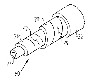
Fig 19 illustrates a further embodiment of an inventional capaci-
tive object in a schematic perspective view. A first band member
26 is arranged in a spiral-shaped path around an axle 27 and
forms a first stratum around the axle. A second band member 28
is arranged in a spiral-shaped path and forms a second stratum
radially outside the first stratum. The two band members 26, 28
CA 02397461 2002-07-12
WO 01/52287 PCT/SE01/00064
are arranged so as to extend in different directions in the cir-
cumference direction of the capacitive object. Furthermore, a
protective sheath 22 is also schematically illustrated. The ar-
rows 29, 57 shown in fig 19 illustrate that the current runs in the
5 longitudinal direction of the respective band member. By ap-
plying the band members around an axle, preferably having a
high resistance to deformation, these band members can be
wound relatively hard around the axle during the production of
the capacitive object. In this way, the risk of air inclusions
10 around the electrically conductive elements is counteracted.
Electrically insulating material in said electrically insulating lay-
ers will be arranged tightly against and at least partly around the
respective electrically conductive element. The core is pref-
erably also flexible in order to make a bending of the capacitive
15 object possible. Such a bending of the capacitive object or a
capacitor produced thereof can be desired for instance for
transport of the same.
Furthermore, a not shown stratum having good insulating prop-
20 erties, for instance in the form of a mica band, is preferably ar-
ranged between these stratums of band members. Such a mica
band consists of a ceramic material, has a high resistance to
penetration of arcs and is high temperature durable. By the
presence of such a stratum having good insulating properties, a
25 breakthrough in a band member is prevented from propagating
into an adjacent band member. ~-
Fig 20 illustrates a further embodiment of the inventional ca-
pacitive object. In contrast to the embodiment in fig 19, the band
members 30, 31 extend in the same direction in the two stra-
tums. This entails that the current is intended to be conducted in
the same direction in the circumference direction of the capaci-
tive object, see arrows 32 , 33, whereby the band members form
a kind of coil. In addition to its capacitance, the capacitive ob-
ject thereby also obtains an essential inductance. The capacitive
object is consequently tuned to a specific frequency. By adapt-
CA 02397461 2002-07-12
WO 01/52287 PCT/SE01/00064
26
ing the inductance to the capacitance, a purely resistive con-
nection can thereby be achieved between two points in a net-
work at a specific frequency. It is realised that the capacitive
object can obtain inductive properties also when it comprises
one single band member 30 arranged in a spiral-shaped path
around an axle 27 and forming a single stratum around the axle.
It is also realised that the capacitive object can obtain inductive
properties also when it comprises more than two band members
arranged in a spiral-shaped path around an axle 27 and forming
more than two stratums around the axle, the band members ex-
tending in the same direction in the different stratums.
The band member 26, 28 and 30, 31 illustrated in fig 19 and 20
form layered structures 60 and 61, respectively.
Fig 21 illustrates a further embodiment of the inventional ca-
pacitive object. An elongated band -34 is wound around a struc-
ture 36 of band members, for instance according to the embodi-
ment in fig 19 and 20. The elongated band 34 of semiconductor
material extends between the two ends of the capacitive object
and constitutes a discharge resistor. Furthermore, a band 35 of
electrically insulating material having a width larger than the
width of the band of semiconductor material is arranged on the
inside of this band. Such an arrangement makes it possible to
dimension the discharge resistance by regulation of the length
of the semiconductor band. This is performed by an overlap
winding of the insulating band with the semiconductor band ar-
ranged along the same. It is realised that the resistance in-
creases with an increasing length of the semiconductor band.
Fig 20 illustrates a schematic circuit diagram over the embodi-
ment in fig 21, the discharge resistor 34 being supposed to be
comprised in a capacitive object of the type shown in fig 20.
Fig 24 illustrates a further embodiment of the inventional ca-
pacitive object. It is here shown that the capacitive object can
CA 02397461 2002-07-12
WO 01/52287 PCT/SE01/00064
27
be provided with a grounded sheath surface in the same way as
conventional cables. A capacitor provided with a grounded
sheath surface can thereby be arranged buried below ground.
This is advantageous in particular since a band of capacitors
built up of such capacitors can be arranged below ground. Such
an arrangement saves space above ground and eliminates the
need of stands for carrying the capacitors according to previous
technique. The capacitor is according to fig 22 provided with,
from the inside and outwards in the radial direction of the ca-
pacitor: a structure 36 of band members, discharge resistor 34,
insulating stratum 37, insulating shield 38, conductive shield, for
instance of copper, 39 and a mechanical protective stratum 40.
Capacitors produced from the above described, inventional ca-
pacitive objects can with advantage be used for the formation of
banks of capacitors. An inventional capacitor can replace a so-
called capacitor unit according to prior art. Such a capacitor unit
was discussed by way of introduction and comprises several ca-
pacitors in the form of rolls. The capacitor rolls are arranged
flattened and piled adjacent to each other in such a capacitor
unit. The height of the layers arranged on each other in the ra-
dial direction of the inventional capacitor is essentially smaller
than the height of a pile of flattened capacitor rolls according to
previous technique. This results in that the mechanic resonance
frequency of the inventional capacitor is essentially lower than
the network frequency and within a frequency range above the
harmonics being most severe as regards resonance amplifica-
tion. This results in a low sound level.
The electrically conductive elements are preferably plate-
shaped, and rectangular. The electrically conductive elements in
two adjacent layers overlap each other with half a partition ac-
cording to the above described examples of layered structures.
Such a relation is preferred, but it is not necessary for the func-
tinning of the capacitor. The electrically conductive elements
should however be at least somewhat displaced in relation to
CA 02397461 2002-07-12
WO 01/52287 PCT/SE01/00064
28
each other in at least two adjacent layers in the longitudinal di-
rection of the layered structure. According to the above de-
scribed examples of layered structures, the electrically conduc-
tive elements have the same shape and size. This is to be pre-
y ferred in order for the capacitor elements to have the same ca-
pacitance, but not necessary for the capacitor to function. By the
capacitor elements having essentially the same capacitance, a
uniform voltage distribution in the network of the capacitor ele-
ments is obtained. In a capacitor according to fig 14-18, the
electrically conductive elements in two respective adjacent lay-
ers can be arranged such that the capacitor elements have es-
sentially the same capacitance due to the fact that the longitudi-
nal direction of the layered structure essentially coincides with
the longitudinal direction of the capacitor. This is also possible,
even though not as prominent, with the embodiments in fig 19-
22 and 24. It can in these cases be achieved for instance in that
the respective layered structure only comprises a low number of
layers of electrically conductive elements. The conductive ele-
ments in two adjacent layers should in that case overlap each
other with half a partition. When the band member is wound
around the axle, and external layer of electrically insulating
material is intended to be more stretched in the longitudinal di-
rection of the band member than a layer located inside this
layer. This stretch makes it possible for the electrically conduc-
tive elements to be arranged with said desired mutual overlap.
The layers of electrically conductive elements extend over es-
sentially the entire length of the layered structure.
The inventional capacitor can be used for direct current as well
as alternating current.
In fig 25 a method for producing a capacitive object according to
the invention is schematically illustrated. Several supplies 41
are arranged, each of which has a roll of a wound dielectric film.
The dielectric film is provided with a layer of several electrically
conductive elements arranged at mutual distances. Possibly, a
CA 02397461 2002-07-12
WO 01/52287 PCT/SE01/00064
29
high-resistance layer is also arranged between the dielectric film
and the layer of electrically conductive elements. Furthermore,
one or several of the supplies 41 can also comprise a roll with a
dielectric film without any layer of electrically conductive ele-
ments. Such a dielectric film is intended to form a barrier layer
in the layered structure. Bands of said dielectric film and said
layers of electrically conductive elements are gradually unwind
from the rolls, redirected and fed to a first station 42. In the sta-
tion 42, the bands are put together and form a layered structure
62 according to any of the above described examples. The lay
ered structure is gradually produced in a feeding direction.
Band members can according to the method be arranged so as
to form a capacitive object according to any of the above de-
scribed embodiments. When a capacitive object is intended to
be produced with band members having a longitudinal direction
essentially corresponding to the longitudinal direction of the
capacitive object, the capacitive object is preferably produced in
a feeding direction essentially corresponding to the feeding di-
rection of the band members. The band members can for in-
stance be guided along an essentially straight lined path and put
together into a layered structure. Two supplies comprise plate-
shaped support members 24. The plate-shaped support mem-
bers are fed forward and arranged on two opposite sides of the
layered structure. In the first station 42, a band of semiconduc-
tor material is wound around the layered structure, and possibly
also around the support members 24, for the achievement of
said discharge resistor. In a second station 43, a protective
sheath is applied around the band. Thereby, a capacitive object
in the form of an elongated cable has been achieved. The ca-
pacitive object can thereafter be cut into desired lengthes de-
pending on the need or the available space. The process of cut-
ting is in the figure indicated with the reference 58. A thus
formed capacitive object can be said to have a capacitance per
unit of length. After cutting into desired length, means 59 for
connection to a voltage can thereafter be arranged at the re-
CA 02397461 2002-07-12
WO 01/52287 PCT/SE01/00064
spective end of a cut capacitive object for the production of the
actual capacitor.
When producing a capacitive object having band members in a
5 spiral-shaped path, the band members are preferably produced
in a first step and wound onto a roll. The roll is arranged on a
rotatable part in a production device. The band member is
thereafter unwound from the roll and applied around an axle
during rotation of the rotatable part. Thereby, the spiral-shaped
10 layered structure is formed. Thereafter, the thus formed capaci-
tive object can be provided with a protective sheath, for instance
of polymeric material. It is of course within the scope of the in-
ventional claims to wind several band members around said
axle.
According to an alternative, the supplies can include rolls with
only dielectric film. In such a case, layers of electrically conduc-
tive elements are applied on the dielectric film after the film has
been unwound from the roll.
With the above mentioned method, the capacitive object is con-
sequently gradually produced in a feeding direction. Preferably,
the production is carried out continuously.
According to an alternative method for producing a capacitive
object, a dielectric film is unwound from a dielectric film roll, and
a layer of electrically conductive elements are applied on the
film. The layer of electrically conductive elements comprises
several rows, for instance eight rows, of electrically conductive
elements, which rows run in the longitudinal direction of the di-
electric film. The electrically conductive elements are preferably
arranged displaced in relation to each other with half a partition
in adjacent rows. Thereafter, the dielectric film is cut in said
longitudinal direction, the cuts being achieved between said
rows of electrically conductive elements. In that way, several,
for instance eight, strips of dielectric film having electrically
CA 02397461 2002-07-12
WO 01/52287 PCT/SE01/00064
31
conductive elements arranged after each other are obtained.
These strips are thereafter arranged lying against each other in
such a way that the respective layer of electrically conductive
elements are arranged separated from an adjacent layer of
electrically conductive elements by a dielectric film. Thereby,
this method does not require any equipment for guiding the
strips in the longitudinal direction of the rows in order to achieve
the desired overlap. For instance, the respective strip is angled
90°, whereupon the strips are brought together to form the lay-
ered structure. Consequently, the strips can in a simple manner
be brought together to form a layered structure comprising a
network of capacitor elements. This layered structure can
thereafter be fed forward in its longitudinal direction so as to
form the capacitive object.
Furthermore, it is within the scope of the inventional claims that
several layered structures are joined along the longitudinal di-
rection of the capacitive object.
When it is desired to produce a capacitive object having a pre-
determined length, it is according to an alternative production
method possible to arrange band members to and fro between
for instance two axles. The positions of these axles thereby form
the ends of the capacitive object.
In case the capacitive object comprises only one band member,
which in its turn only comprises one layer of several electrically
conductive elements and only one adjacent layer of electrically
insulating material, the band member is arranged so as to ex
tend to and fro between the ends of the capacitive object.
In fig 26 a bank of capacitors 44 for series compensation is il-
lustrated: The bank of capacitors is built up of several inven-
tional capacitors. The series compensation device comprises
three sets of capacitors 45, 46, 47. Each of the sets is intended
CA 02397461 2002-07-12
WO 01/52287 PCT/SE01/00064
32
for one of the three phases of the network. The sets of capaci
tors are arranged hanging in the air between two stands 48, 49.
In fig 27 a bank of capacitors 50 in the form of a so-called shunt
bank is illustrated. The bank of capacitors is built up of several
inventional capacitors. The bank of capacitors 50 comprises
three sets of capacitors 51, 52, 53: each set being intended for
one of the three phases of the network. The capacitors are ar-
ranged hanging from a stand 54.
The respective inventional capacitor of the sets of capacitors in
fig 26 and 27 should be compared with a capacitor unit accord-
ing to prior art. The construction of such a capacitor unit has
been described above. In the light of the description above, it is
realised that the inventional capacitor has an essentially simpli
fied construction. Furthermore, an essentially simplified produc
tion, transport and assemblage is made possible. The banks of
capacitors according to fig 26 and 27 furthermore, in relation to
conventional banks of capacitors, require an essentially smaller
space as regards ground surface.
Fig 28 illustrates a first embodiment of an electric device 70
having capacitive as well as inductive properties, which device
here is intended to constitute a filter. A section of a capacitive
object 71 of the type illustrated in fig 15 or 16 is here wound in a
spiral-shaped path. Owing to the capacitive object 71 being ar-
ranged to conduct current in its longitudinal direction, an induc-
tive element 72 in the form of a coil is formed. The filter 70 also
comprises a core 73 of magnetically well conductive material.
The capacitive object 71 is partly wound around two legs 74 of
the core 73.
In fig 29 a schematic, partly cut sectional view of the filter 70 in
fig 28 is illustrated. The core has an air gap 75 between said
legs 74. The air gap 75 is intended to receive a magnetic energy
generated when the capacitive object is connected to a voltage
CA 02397461 2002-07-12
WO 01/52287 PCT/SE01/00064
33
source. In the electric device 70 in fig 28, the capacitive object
71 consequently forms an inductive element in form of a coil.
The two properties are however integrated into one single com
ponent. This is schematically illustrated in a circuit diagram in
fig 30.
Fig 31 illustrates a variant of the electric device illustrated in fig
28 and 29. An electric resistor 76 is magnetically connected to a
magnetic flux generated when the capacitive object 71 is con-
nected to a voltage source. The resistor 76 is here connected to
the iron core 73 via an electric line wire arranged around the
core. When the current is conducted in a spiral-shaped path, a
magnetic flux is generated in the core inside the turns of the ca-
pacitive object 71. This flux gives rise to a current through the
line wire, which current will flow through the resistor 76. The re-
sistor 76 thereby functions as a damping resistor.
The electric device according to the invention, which has ca-
pacitive as well as inductive properties, can of course comprise
other types of capacitive objects in the form of cable-shaped
conductors than the ones illustrated in fig 28-31. The capacitive
object 71 can for instance advantageously be of the type illus-
trated in fig 17, in which case the capacitive object is wound in
such a way that the perpendiculars to the layers in the layered
structure are essentially perpendicular to a geometric centre line
of the coil. Owing to the wave-shape of the layered structure,
the effect of a compressive stress in the layers arranged in
wards, towards the centre line, is mitigated, which reduces the
risk of folding of these layers. Such a folding could cause air
pockets, which in their turn could cause glow.
The capacitive object 71 included in the inventional electric de-
vice can also advantageously be of the type illustrated in fig 18,
in which case the occurrence of foldings in the sections of the
layers of the layered structure being subjected to compressive
CA 02397461 2002-07-12
WO 01/52287 PCT/SE01/00064
34
stress is reduced during winding of the capacitive object into
coil-shape in the same way as in the previous example.
The capacitive object included in the inventional electric device
can also advantageously be of the type illustrated in fig 20, in
which case the capacitive object does not have to be wound into
coil-shape to obtain inductive properties, since a capacitive ob-
ject of this type has inductive properties also in a rectilinear
state. An electric device comprising a capacitive object of this
type is tuned to a specific frequency. By adapting the inductance
to the capacitance, a purely resistive connection can thereby be
achieved between two points in a network at a specific fre-
quency.
Fig 32 illustrates an arrangement for filtering harmonics. A recti
fier 77 is arranged to rectify alternating current from an alter
nating voltage source 78 into direct current. Three filters 79 are
connected in parallel with the rectifier 77 for the purpose of fil
tering one harmonic each. The filters 79 suitably comprise ca
pacitive objects of the type illustrated in fig 20.
Fig 33 illustrates several electric resistors 80 in the form of
electric resistor wires. Each of the electric resistor wires 80 ex-
tends around a layered structure, and in the case shown in fig
33 around the capacitive object 81. Means 82 are also arranged
for maintaining the distance between each of the resistor wires
80 and internally located, heat sensitive parts of the capacitive
object. The distance means 82 are preferably formed of a high
temperature durable material and arranged in such a way that a
low heat transfer is obtained between the resistor wires and the
internally located, heat sensitive parts of the capacitive object.
For instance, they comprise a ceramic material. In the case il-
lustrated in fig 33, the distance means are designed in such a
way that air-cooling is achieved in the space between each of
the resistor wires and the capacitive object 81. It is of course
also within the scope of the inventional claims that the resistors
CA 02397461 2002-07-12
WO 01/52287 PCT/SE01/00064
80 are arranged inside the sheath of the capacitive object 81.
The resistors 80 will consequently be magnetically connected to
a magnetic flux generated by a current through the capacitive
object. This is schematically illustrated in fig 34. The invention
5 is of course not in any way limited to the preferred embodiments
described above, on the contrary, a number of possibilities to
modifications thereof should be obvious to a man skilled in the
art, without departing from the basic idea of the invention as de-
fined in the appended claims.
15