Note : Les descriptions sont présentées dans la langue officielle dans laquelle elles ont été soumises.
CA 02399007 2002-07-30
WO 01/71384 1 PCT/SE01/00556
A METHOD AND A DEVICE FOR RADIOGRAPHY AND A RADIATION DETECTC=_
FIELD OF THE INVENTION
The invention relates to a method and apparatus for obtaining
radiography images. Moreover it relates to a detector for
detecting incident radiation.
BACKGROUND OF THE INVENTION
X-rays have been used in radiographic imaging for a long time,
and have been subject to great developments. In its simplest
form, imaging is conducted by providing a source of X-ray
radiation, an object to be imaged, through which the radiaticn
is transmitted, and a detector for the detection and recordinc
of the transmitted radiation. The X-ray detector used today,
at hospitals, is normally a screen-film combination. In a
phosphor screen (e.g. Gd2OZS), X-ray photons are converted and
thereby produce secondary light, which is registered on a
photographic film. The use of a film limits the dynamic range
of the image. The increased efficiency achieved by using a
phosphor screen is provided at the expense of the resolution,
since the secondary light is emitted isotropically.
To visualise an object within an image, it is necessary tha-_
the signal to noise ratio exceeds a certain threshold. The
ideal system would have the image noise determined only by
photon statistics. This is typically not the case for systems
operating with a screen-film combination. To obtain a useful
diagnostic image one must increase the patient dose of X-ray
radiation.
X-ray photon flux is, by nature, digital. However, one has to
distinguish between two different methods in producing digita=
images:
- Integrating technique is an intrinsically analogue method.
The response in each pixel is proportional to the total X-
CA 02399007 2002-07-30
WO 01/71384 2 PCT/SE01/00556
ray energy flux. The image is then built up digitally by
means of the pixels. Examples of the integrating approach to
imaging are CCD (charge-coupled device), storage phosphors,
selenium plates, etc. The dynamic range of many of these
"digital" detectors is similar to that of film. As in the
film technique, the photon flux energy (not the number of
photons) is integrated, and thus add noise, since X-ray
tubes produce a wide energy spectrum. The most significant
noise sources are the "dark current" and the fluctuations in
photon energy.
- Photon counting is an intrinsically digital method, in which
each photon is detected, and detection signals are counted
A two-dimensional photon counting detector requires many
readout elements, and a huge number of interconnections. This
leads to typical manufacturing and reliability problems, which
has been experienced in such systems. It is difficult to make
a large two-dimensional detector with high resolution and high
probability for interaction of a major fraction of the X-ray
photons.
One way to overcome size and cost limitations, in connection
with two-dimensional detector readout systems, is to create an
image receptor that is essentially one-dimensional and
acquires the second dimension for the image by scanning the X-
ray beam and detector across the object to be imaged. Scanning
can be done by employing a single line detector and a highly
collimated planar X-ray beam. In addition, this approach
eliminates the scattered radiation noise but imposes a large
heat load on the X-ray tube. To ease the tube loading and
simplify the mechanics (by reducing the scanning distance), a
multi line set of low cost one-dimensional detectors is
beneficial.
One advantage with a line detector is a significant reduction
of image noise, which is caused by radiation scattering in the
CA 02399007 2002-07-30
WO 01/71384 3 PCT/SEOI/00556
object to be imaged. An X-ray photon that is Compton-scattered
in the object will not be detected in a line detector.
Several attempts have been made to develop a photon counting
X-ray imaging system based on the scanning technique. This
requires detectors that produce fast signals with a rise time
of a few nanoseconds. Only a few detection media can produce
signals that fast, e.g. a gas or a semiconductor (for example
silicon). Semiconductor detectors are expensive and are thus
not practical in a multi line configuration. In a gas medium,
an X-ray photon interacts with a gas atom which emits a
primary ionisation electron, which in turn produces electron-
ion pairs that are further multiplied in a gas avalanche. The
advantage of a gas detector is low cost, a high noiseless
signal amplification in the gas (up to 106) , and a uniformity
of the detection media.
Several imaging systems described in published articles
utilise a multi wire proportional chamber as detector. In its
basic configuration, the multi wire proportional chamber
consists of a set of thin anode wires stretched between, and
parallel with, two cathode planes. Application of a voltage
between the anode wires and the cathode planes creates an
electric field in the chamber. Electrons emitted in the gas by
ionisation of gas atoms, caused by incident X-ray photons,
drift towards the anode wires, and when approaching the thin
wires they experience ionising interactions, with gas
molecules, in the strong electric field. The ensuing avalanche
multiplication provides a noiseless amplification of the
charge signal, by a factor as large as 105 or more.
An example of a digital imaging system based on photon
counting is described in the article, "Multi wire proportional
chamber for a digital radiographic installation", by S. E.
Baru et. al., in Nuclear Instruments and Methods in Physics
Research A, vol. 283 (Nov. 10 1989), pages 431- 435. This
detector is a combination of a drift chamber and a multi wire
CA 02399007 2002-07-30
WO 01/71384 4 PCT/SE01/00556
proportional chamber with non-parallel anode wires aiming at
the focal point of the X-ray source. The radial wires enable
the use of a thick interaction volume without parallax error.
The uniformity of gain along the anode wires is guaranteed by
an increasing gap between the anode wires and the cathode
planes.
The described device has, however, the following drawbacks.
The need for providing sufficient space for wire mounting and
high voltage isolation results in losses of X-ray detection
efficiency.
The use of radial wires to solve the parallax problem results
in a position resolution limited by the smallest practical
anode wire pitch of about 1 mm. The problem can be overcome by
using cathode strip readout that provides the ultimate multi
wire proportional chamber resolution. One possibility of a
practically feasible fast cathode strip readout is described
in the article, "The OD-3 fast one-co-ordinate X-ray
detector", by V. M. Aulchenco et. al., in Nuclear Instruments
and Methods in Physics Research A, vol. 367 (Dec. 11, 1995),
pages 79- 82. In this solution, an increasing anode- cathode
gap is combined with a decreasing high voltage applied to
different anode wire groups.
A known problem with using multi wire proportional chambers
for medical imaging is the space charge effect that degrades
the detector performance at high X-ray fluxes above 10 kHz/mmz.
To decrease the space charge effect, the anode plane has been
modified by adding alternating cathode wires in a prior art
device, disclosed in US-A-5 521 956 (G. Charpak).
The use of thin wires (typically less than 100 m in diameter)
in multiwire proportional chambers makes them difficult to
construct, and reduces reliability, since one broken wire
disables operation of the whole detector.
CA 02399007 2002-07-30
WO 01/71384 5 PCT/SEOI/00556
A gas avalanche detector that is very simple in construction
and does not use anode wires is the gaseous parallel plate
avalanche chamber. This detector is basically a gas-filled
capacitor, comprising two essentially parallel conducting
plates, an anode and a cathode, subjected to a high voltage.
The high voltage is chosen such that electrons released by
ionisation in the gas produce avalanches in a strong electric
field between the plates. Typically, the distance between the
plates is on the order of one millimetre, and the field
strength is in the order of kilovolts per millimetre,
depending on the type of gas used. A wide variety of gases can
be used depending on the application. In such a detector X-ray
photons are incident on a plane parallel to the detector
plane, or on the cathode, which is made of a material that
emits electrons, so called photoelectrons, when X-ray photons
interact with it.
An important advantage over the multi wire proportional
chamber, is that the electrostatic field in a gaseous parallel
plate avalanche chamber is not concentrated around single thin
wires, but is essentially constant over the entire
amplification volume. This results in a very short drift time
of positive ions across the amplification gap, thus
drastically reducing the space charge effect.
An example of using a gaseous parallel plate avalanche chamber
for radiographic imaging is described in the article, "A
parallel plate chamber with pixel readout for very high data
rate", by F. Angelini et. al., in IEEE Transactions on Nuclear
Science, vol. 36 (February 1989) pages 213- 217. In the two-
dimensional readout configuration described, it is difficult
to achieve high X-ray conversion efficiency despite the
addition of a drift chamber in front of a parallel plate
chamber to increase the thickness of the gas layer.
Another device, disclosed in US-A-5 308 987 (Wuest et. al.),
utilises a cathode made of a high atomic number material to
CA 02399007 2002-07-30
WO 01/71384 6 PCT/SE01/00556
improve the conversion efficiency in a parallel plate chamber
used in a two-dimensional readout configuration. The low yield
of photoelectrons from the high acomic number material results
in a reduction of X-ray ray detection efficiency.
Another important difference from a multi wire proportional
chamber is that the gas amplification factor strongly depends
on the distance from the primary ionisation charge to the
anode, resulting in a poor energy resolution and signal
detection efficiency, in prior used gaseous parallel plate
avalanche chambers. Due to this problem, prior devices were
unable to use the gas amplification gap in gaseous parallel
plate avalanche chambers as an X-ray conversion volume.
In SE 9704015-8 this limitation been overcome by providing a
well collimated planar beam incident essentially sideways on
the detector.
A general drawback with gaseous X-ray detectors relates to the
fact that the X-ray flux coming from the X-ray source is
divergent. In a thick conversion volume this divergence causes
a parallax error. Most methods proposed to minimise the
parallax error are difficult to implement in practice.
In US 5 614 722 it is disclosed that the gaseous medium in a
radiation detector can be replaced with a liquid such as, for
example, liquid argon or liquid xenon. However, there is no
teaching how to obtain liquid argon or xenon. Since liquid
argon has a boiling point of -186 C and liquid xenon has a
boiling point of -107 C this means that the gas in the
detector either has to be cooled to below said temperatures or
pressurized or both. If the gas in the detector is pressurized
the thickness of material of the walls and of the entrance of
radiation of said detector has to be increased. The X-ray
photons will therefore to some extent be adsorbed in the
entrance material which results in a reduction of the X-ray
detection efficiency.
CA 02399007 2008-02-12
7
SUMMARY OF THE INVENTION
It is an object of the present invention to provide a method, an
apparatus and a detector for use in radiography, which overcomes
the above-mentioned problem.
Certain exemplary embodiments may provide a method for obtaining
a radiography image, said method comprising the steps of:
emitting X-rays from an X-ray source into a chamber in any
direction of a half sphere, which is symmetric around a normal
vector of a cathode plan, with respect of a cathode or an anode
in electrode arrangements; transmitting said X-rays through an
object to be imaged; detecting the X-rays transmitted through
said object in said chamber, the depth of which, in the direction
of the incident radiation, is such as to permit interaction of
the incident X-ray photons with atoms of a liquid, at a
temperature between -30 C and room temperature, or solid
material in said chamber, for the production of primary
ionization electron-ion pairs, within a detector including said
electrode arrangements between which a voltage is applied for
creating an electrical field; applying the voltage to said
electrode arrangements in said detector for creating an
electrical field which causes electron-ion avalanches of primary
and secondary ionization electrons released by said incident
X-ray photons; and detecting electrical signals in at least one
detector electrode arrangement, said electrical signals being
induced by said electron-ion pairs, in at least one of a
plurality of detector electrode elements arranged adjacent to
each other.
CA 02399007 2008-02-12
8
Certain other exemplary embodiments may provide an apparatus
for use in radiography, comprising: an X-ray source, wherein
emitted X-rays from the X-ray source enter a chamber from any
direction of a half sphere, which is symmetric around a normal
vector of a cathode plan, with respect to a cathode or anode
in electrode arrangements; a chamber, the depth of which, in
the direction of the incident radiation, is such as to permit
interaction of the incident X-ray photons with atoms of a
liquid, at a temperature between -30 C and room temperature,
or solid material in said chamber, for the production of
primary ionization electron-ion pairs, within a detector
including said electrode arrangements between which a voltage
is applied for creating an electrical field for detecting the
X-ray photons transmitted through said object; and a plurality
of detector electrode elements being arranged adjacent to each
other.
Still certain other exemplary embodiments may provide a
detector for detecting incident radiation, comprising:
electrode arrangements between which a voltage is applied for
creating an electrical field; a chamber, the depth of which,
in the direction of the incident radiation, is such as to
permit interaction of the incident X-ray photons with atoms of
a liquid, at a temperature between -30 C and room
temperature, or solid material in said chamber, said emitted
X-rays from the X-ray source entering the chamber from any
direction of a half sphere, which is symmetric around a normal
vector of a cathode plan, with respect to a cathode or anode
in said electrode arrangements, for the production of primary
ionization electron-ion pairs, within a detector including
CA 02399007 2008-02-12
8a
electrode arrangements between which a voltage is applied for
creating an electrical field for detecting the X-ray photons
transmitted through said object, said voltage applied between
said electrode arrangements in said detector being high enough
for creating an electrical field which causes electron-ion
avalanches of primary and secondary ionization electrons
released by said incident X-ray source; and a plurality of
detector electrode elements arranged adjacent to each other.
Yet another exemplary embodiment may provide an apparatus for
use in planar beam radiography, comprising: a radiation
source, for emitting an incident radiation source; and a
gaseous avalanche detector, including a chamber into which the
incident radiation is emitted so that the radiation enters the
chamber and the incident radiation interacts with atoms of a
liquid, at a temperature between -30 C and room temperature,
or solid material in the chamber for the production of primary
ionization electron-ion pairs, within the gaseous avalanche
detector and a mesh, arranged between and substantially
parallel to a first and a second plate, wherein a voltage is
applied between a first of at least two electrode arrangements
and the mesh, in order to create a conversion and drift volume
and an amplification volume.
Still another exemplary embodiment may provide an apparatus
for use in planar beam radiography, comprising: a radiation
source, for emitting an incident radiation source; and a
gaseous avalanche detector, including a chamber into which the
incident radiation is emitted so that the radiation enters the
chamber and the incident radiation interacts with atoms of a
liquid, at a temperature between -30 C and room temperature,
or solid material in the chamber for the production of primary
CA 02399007 2008-02-12
8b
ionization electron-ion pairs, within the gaseous avalanche
detector.
Yet a further exemplary embodiment may provide an apparatus
for use in planar beam radiography, comprising: a radiation
source, for emitting an incident radiation source; and a
gaseous avalanche detector, including a chamber into which the
incident radiation is emitted so that the radiation enters the
chamber substantially sideways between a first and a second
essentially parallel plate, and in which a voltage is applied
for creating an electrical field, wherein the electrical field
causes electron-ion avalanches of primary and secondary
ionization electrons released by the incident radiation,
wherein the incident radiation interacts with atoms of a
liquid, at a temperature between -30 C and room temperature,
or solid material in the chamber for the production of primary
ionization electron-ion pairs, within the gaseous avalanche
detector.
An advantage of the present invention is that the detector
exhibits fast response with pulse widths less than 10
nanoseconds and as fast as 1 nanosecond.
Another advantage of the present invention is that the
detector can be made thinner compared to a similar gaseous
detector.
Yet another advantage of the present invention is that the
detector is less sensitive to the direction of the incident
X-rays compared to similar gaseous detectors with respect to the
CA 02399007 2002-07-30
WO 01/71384 9 PCT/SE01/00556
resolution of the image from the radiated object detected by
the detector.
Further objects and advantages are attained by further
features in the appended claims.
BRIEF DESCRIPTION OF THE DRAWINGS
Fig. 1 illustrates schematically, in an overall view, an
apparatus for planar beam radiography, according to the
invention,
Fig. 2 is a schematic cross sectional view of a first
embodiment of a detector chamber according to the
invention,
Fig. 3 is a schematic cross sectional view of a detector
chamber, according to the invention, contained in a
housing.
Fig. 4 is a schematic top view of a first embodiment of an X-
ray source and an electrode formed by readout strips,
Fig. 5 is a schematic top view of a second embodiment of an X-
ray source and an electrode formed by segmented readout
strips,
Fig. 6 is a schematic cross sectional view of a second
embodiment of a detector chamber according to the
invention,
Fig. 7 is a schematic cross sectional view of an embodiment
according to the invention, with stacked detectors
Fig. 8 is a schematic cross sectional view of a further
embodiment according to the invention, with stacked
detectors.
DESCRIPTION OF PREFERRED EMBODIMENTS
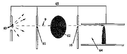
Fig. 1 is a sectional view in a plane orthogonal to the plane
of a planar X-ray beam 9 of an apparatus for planar beam
radiography, according to the invention. The apparatus
includes an X-ray source 60, which together with a first thin
collimator window 61 produce the planar fan-shaped X-ray beam
CA 02399007 2002-07-30
WO 01/71384 10 PCT/SE01/00556
9, for irradiation of an object 62 to be imaged. The first
thin collimator window 61 can be replaced by other means for
forming an essentially planar X-ray beam, such as an X-ray
diffraction mirror or an X-ray lens etc. The beam transmitted
through the object 62 enters a detector 64, optionally through
a thin slit or second collimator window 10, which is aligned
with the X-ray beam. A major fraction of the incident X-ray
photons are detected in the detector 64, which includes a
detector chamber, oriented, in this embodiment, so that the X-
ray photons enter sideways between, and essentially parallel
with two essentially parallel plates. The X-ray photons may
alternatively enter the detector chamber from any direction of
a half sphere 17 which is symmetric around a normal vector of
the cathode plan as shown for example in figure 2.
The detector and its operation will be further described
below. The X-ray source 60, the first thin collimator window
61, the optional collimator window 10 and the detector chamber
64 are connected and fixed in relation to each other by, for
example, a frame or support 65. The so formed apparatus for
radiography can be moved as a unit to scan an object which is
to be examined. In a single detector system, as shown in Fig.
1, the scanning is preferably done by a pivoting movement,
rotating the unit around an axis through for example the X-ray
source 60 or the detector 64. The location of the axis depends
on the application or use of the apparatus, and possibly the
axis can also run through the object 62, in some applications.
An apparatus and a method according to this invention is
especially advantageous in imaging a part of a body of a
patient, e.g. in mammography.
The detector chamber, is generally composed of two essentially
parallel plates constituting two limiting walls of the
chamber. Said plates are subjected to a strong electric field,
which is generated by applying a high voltage. A volume
defined as a region or gap between said plates is filled with
CA 02399007 2002-07-30
WO 01/71384 11 PCT/SEOI/00556
a liquid material, at a temperature between -30 C and room
temperature, or a solid material.
An X-ray photon incident into the liquid material, at a
temperature between -30 C and room temperature, or solid
material produces an electron-ion pair upon interaction with
an atom in said volume. This production may be caused by photo
effect, Compton-effect or Auger-effect. The primary electron
so produced loses its kinetic energy through interactions with
new atoms, causing the production of further new electron-ion
pairs, typically a few hundreds, whereof the electrons are
called secondary ionisation electrons.
The secondary ionisation electrons may then be amplified by
electron-ion avalanches depending on the strength of the
electric field. When the electric field between the plates is
low, no (or very little) electron-ion avalanche amplification
takes place. Above a well defined electric field strength
electron-ion avalanche amplification can start and can reach
amplifications up to 100 or more. The electric field is
preferably in the region to cause avalanche amplification, but
the present invention will also work for said lower electrical
field range, i.e. not high enough to cause electron-ion
avalanches.
The movements of the electrons and ions induce electrical
signals in the electrodes. Those signals are typically picked
up in one or both of the electrodes and are further amplified
and processed by a readout circuitry to obtain an accurate
measurement of the X-ray photon interaction point and,
optionally the X-ray photon energy.
In a preferred embodiment of the invention, the X-rays to be
detected are incident sideways on the detector in a direction
essentially parallel to the parallel plates, and may enter the
detector through a thin slit or collimator window in case of
liquid material, at a temperature between -30 C and room
CA 02399007 2002-07-30
WO 01/71384 12 PCT/SE01/00556
temperature, between said plates. Said thin slit or collimator
window may be omitted in the case of solid material between
said plates. In this way the anode and/or the cathode plates
does not have to be pervious to the X-ray photons. In an
alternative embodiment of the invention, the X-rays to be
detected are incident anywhere from a half sphere with respect
to one of the plates on the detector. This alternative
embodiment may require that the cathode plates are, at least
to some degree, pervious to the X-ray photons, since the X-
rays may go through said cathode in order to interact with the
material in the detector chamber.
Referring to Fig. 2, a first embodiment of a detector
according to the invention, is shown, and designated the
reference number 64. This detector chamber includes an anode
plate 1 and a cathode plate 2, being mutually essentially
parallel and separated by a thin gap or region 13 defining as
mentioned above a volume. Said volume is filled with a liquid
material at a temperature between -30 C and room temperature
or a solid material, being for example TMP (Trimethylpentane)
TME (Trimethylethane), cadmium zinc telluride (CdZnTe),
silicon, germanium or other types of semiconductors.
The anode plate 1 includes a substrate 3, made of for example
glass or ceramics, having a thickness of preferably 0.1 - 10
mm, and an anode electrode 4 arranged thereon in the form of a
coating of a conductive material, for example metal, having a
thickness of preferably 0.01- 10 m.
For better adhesion to the substrate 3 and for better layer
stability, the electrode 4 may include several metal layers,
each with a different thickness and material, for example
vanadium, copper and nickel. When the substrate 3 is made of
glass, the first layer is preferably of chromium, which has
good adhesion properties to glass as well as to the subseauent
metal layers. The electrode 4 may also include a layer of
CA 02399007 2002-07-30
WO 01/71384 13 PCT/SEOI/00556
resistive material, for example silicon monoxide, deposited on
top of the metal layer(s).
Likewise, the cathode plate 2 includes a substrate 6 with a
coating 5, similar to what is described about the anode 1.
Both the anode electrode 4 and the cathode electrode 5 can be
segmented into strips parallel and/or orthogonal to the
incoming X-ray beam.
The important characteristics of the liquid material, at a
temperature between -30 C and room temperature, or solid
material is on the first hand that said materials are capable
of being ionised when influenced by X-ray photons and on the
other hand that said materials exhibit a relatively low
electron affinity. Low electron affinity makes it possible for
an electron to travel a long distance without being absorbed.
The anode electrode 4 and the cathode electrode 5 are
connected to a high voltage DC power supply 7, for producing a
uniform electric field 8, in the gap or region 13 between the
essentially parallel plates 1 and 2. As an example, the gap or
region 13 has a height D (distance between the parallel plates
1 and 2) of 10-1000 m, and the voltage V applied between the
electrodes 4 and 5 is 1000-100,000 V. The voltage applied
creates an electric field E between the electrodes 4 and 5,
that is equal E=V/D.
In operation, X-rays 9 are incident on the detector 64 from
any direction of a half sphere with respect to a cathode 2 or
an anode 1 in said electrode arrangements. In figure 2 the X-
ray photons are incident on the detector by essentially
sideways. The incident X-rays 9 enter the detector 64 through
an optional thin slit or collimator window 10 close to the
cathode plate 2, and travel through the volume in a direction
essentially parallel to the cathode plate 2. X-ray photons
produce a primary ionisation electron-ion pair within the
volume as a result of interaction with an atom of the liquid
CA 02399007 2002-07-30
WO 01/71384 14 PCT/SE01/00556
material, at a temperature between -30 C and room temperature,
or solid material therein. Each primary electron 11 produced
loses its kinetic energy through interactions with atoms
causing further production of electron-ion pairs (secondary
ionisation electron-ion pairs). Typically a few thousand
secondary ionisation electron-ion pairs are produced from a 20
keV X-ray photon in this process. The secondary ionisation
electrons 16 (together with the primary ionisation electron
11) are accelerated in the high electric field, in a direction
towards the anode plate 1. The accelerated electrons 11, 16
interact with other atoms in the gap 13 causing further
electron-ion pairs to be produced. Those produced electrons
will also be accelerated in the field, and will interact with
new atoms, causing further electron-ion pairs to be produced.
This process continues during the travel of the electrons
towards the anode 1 and an avalanche 12 will be formed.
For primary ionisation electrons emitted at a distance H from
the anode 1, the overall charge gain is given by M= exp(aH),
where a is the first Townsend coefficient pertinent to the
liquid material, at a temperature between -30 C and room
temperature, or solid material and field conditions. Under
proper choices of material, e.g. one of those mentioned above,
and electrical field, gains from 2-100 and more can be
achieved. Under the influence of the strong electric field,
the electrons in the avalanche volume will move towards the
anode, while the ions will move towards the cathode 2. Due to
the fact that the strong electric field is uniform over the
gap and the height D of the gap 13 is very small, a very short
drift time of the positive ions across the amplification
volume is achieved, which drastically reduces space charge
effects.
The movement of charges in the gap 13 induces electrical
charges on the anode electrode 4 as well as on the cathode
electrode S. The induced charges can be detected, for example,
by means of the anode electrode 4 coupled to a charge
CA 02399007 2002-07-30
WO 01/71384 15 PCT/SEOI/00556
sensitive pre-amplifier, which converts the charge pulses into
a current or voltage pulse that can be further processed in
processing electronics 14, also including said pre-amplifier.
Possibly, the cathode electrodes or a separate der-ector
electrode arrangement can be used for the detection in a
similar way.
It is to be noted that each incident X-ray photon that
interacts with an atom will cause an avalanche 12, which is to
be detected if the applied electrical field is hiah enough. In
order to achieve a high detection efficiency where a major
fraction of the X-ray photons causes avalanches, the length of
the detector chamber, in the direction of the incident X-ray
photons, must be chosen to give a high probability for
interaction between the X-ray photons and atoms of the
material in the volume 13. The probability of interaction
increases with increasing length of the gaseous parallel plate
avalanche chamber. The definition of length is either the
orthogonal distance between the plates, the length of the
detector as measured parallel with said plates or a distance
being neither orthogonal or parallel with said plates.
As mentioned, the detector chamber 64 contains a solid
material or liquid material, at a temperature between -30 C
and room temperature. Therefore, in case of liquid material at
a temperature between -30 C and room temperature, the detector
includes a leak-proof housing 91 with a slit entrance window
92, through which the X-ray beam 9 enters the detector, as
illustrated in Fig. 3. The window is made of a material which
is essentially transparent to the radiation, e.g. Mylar , or a
thin aluminium foil. This is a particularly advantageous
additional effect of the invention, detecting essentially
sideways incident beams in the detector chamber 64, compared
to detector chambers, which are designed for radiation
incident substantially perpendicular to the parallel plates or
in any direction of a half sphere with respect to the cathode
2 or anode 1, requiring a window covering a large area or a
CA 02399007 2002-07-30
WO 01/71384 16 PCT/SEOI/00556
cathode material pervious to said X-rays. The window 92 can in
this way be made thinner, thus reducing the number of X-ray
photons absorbed in the window 92 or absorbed by the cathode
material.
The electrode arrangement shown in Fig. 4 is preferably the
anode 1, but alternatively or conjointly the cathode 2 can
have the described construction. In the alternative embodiment
of Fig. 3 the detector electrode arrangement 15 may be formed
as shown in Fig. 4. In that case, the anode electrode 4 is
formed as an unitary electrode without strips and spacings.
The same is valid for the cathode electrode or the anode
electrode, respectively, when only the other thereof comprises
the detector electrode arrangement.
In Fig. 5, an alternative configuration of an electrode is
shown. The strips have been divided into segments 21,
electrically insulated from each other. Preferably a small
spacing extending perpendicular to the incident X-rays is
provided between each segment 21 of respective strip. Each
segment is connected to the processing electronics l4 by means
of signal conductors 22, where the signals from each segment
preferably are processed separately. As in Fig. 4, where the
anode or cathode electrode constitute the detector electrode,
the signal conductors 22 also connect the respective strip(s)
to the high voltage DC power supply 7.
This electrode can be used when the energy of each X-ray
photon is to be measured, since an X-ray photon having higher
energy statistically causes a primary ionisation after a
longer path through the material than an X-ray photon of lower
energy. By means of this electrode, both the position of X-ray
photon interaction and the energy of each X-ray photon can be
detected.
Generally in all embodiments, each incident X-ray photon
causes one induced pulse in the detector electrode. The pulses
CA 02399007 2002-07-30
WO 01/71384 17 PCT/SEOI/00556
are processed in the processing electronics, which eventually
shapes the pulses, and integrate or count the pulses from each
strip representing one pixel. The pulses can also be processed
so as to provide an energy measure for each pixel.
Where the detector electrode is on the cathode side the area
of an induced signal is broader (in a direction perpendicular
to the direction of incidence of the X-ray photons) than on
the anode side. Therefore, weighing of the signals in the
processing electronics is preferable.
The fact that the amplitude of an induced signal to be
measured, which is a result of an interaction between an X-ray
photon and an atom of the material in the volume 13, strongly
depends on the distance from the starting point of the
avalanche to the anode electrode, places demands on the
alignment of the collimator windows 61, 10 and the anode
electrode 4. The desired condition is a planar beam parallel
with the anode electrode. These tight demands can be eased by
a detector with a configuration shown in Fig. 6.
An electrically conductive mesh or grid 51 arranged between
and essentially parallel with the anode and the cathode
plates, divides the gap into a drift chamber 52 for X-ray
conversion and a parallel plate avalanche chamber 53 for
amplification. Both chambers may be filled with the same
liquid material, at a temperature between -30 C and room
temperature, and the separating mesh serves as a cathode for
the parallel plate avalanche chamber 53, and as an anode for
the drift chamber 52. If solid material is in the volume 13
the mesh is either integrated in said semi-conducting material
or in between two separated parts of said solid material
preferably in a low pressure environment.
A weak electric field is created between the cathode electrode
5 and the mesh 51 by means of the power supply 7. In this weak
field, the secondary ionisation electrons produced by the
CA 02399007 2002-07-30
WO 01/71384 18 PCT/SE01/00556
primary ionisation electrons (together with the same) can
drift towards the mesh 51. A high voltage is further applied
between the mesh 51 and the anode electrode 4, which results
in a strong electric field. This field may attract the
electrons to pass through the mesh 51, and passing the mesh 51
they may start an electron-ion avalanche 12, as described
above. The other parts of the detector are also the same as
described above. It is important that the distance between the
mesh 51 and the anode electrode is essentially uniform, since
the amplification is strongly dependent on the distance from
the starting point of the avalanche, here the mesh 51, to the
anode electrode. The alignment of the X-ray beam 9 and the
parallelity of the cathode electrode is not critical.
Fig. 7 shows schematically an embodiment of the invention with
a plurality of the inventive detectors 64 stacked, one on top
of another. By this embodiment a multiline scan can be
achieved, which reduces the overall scanning distance, as well
as the scanning time. The apparatus of this embodiment
includes an X-ray source 60, which together with a number of
collimator windows 61 produce a number of planar fan-shaped X-
ray beams 9, for irradiation of the object 62 to be imaged.
The beams transmitted through the object 62 optionally enter
the individual stacked detectors 64 through a number of second
collimator windows 10, which are aligned with the X-ray beams.
The first collimator windows 61 are arranged in a first rigid
structure 66, and the optional second collimator windows 10
are arranged in a second rigid structure 67 attached to the
detectors 64, or arranged separately on the detectors.
By choosing the angle cx between the anode plate 1 and the
cathode plate 2 of each detector, the detectors can be stacked
with the surfaces of the detectors facing each other being
parallel, when the detectors are aligned with the X-ray
source. This facilitates the manufacturing of the multiline
detector, since no special steps for aligning and adjustment
is needed. The stability of the detector is also increased,
CA 02399007 2002-07-30
WO 01/71384 19 PCT/SEOI/00556
while the number of parts is reduced. Preferably the stacked
detectors are accommodated in one common housing 91. It can
be advantageous if the cathodes 2 of the two adjacent
detectors face each other, and that the anodes 1 of two
adjacent detectors face each other. In such a case the
cathodes and/or anodes of two adjacent detectors can be formed
into common elements for two adjacent detectors. If they are
accommodated in separate housings also the outer walls of each
housing exhibit an angle a (i.e. one wall is parallel with the
anode plate 1 and one wall is parallel with the cathode plate
2).
Said angle a is in the range of 0<a!590, preferably l/1600-60
The X-ray source 60, the rigid structure 66, and the possible
structure 67 including collimator windows 61, 10,
respectively, and the stacked detectors 64, which are fixed to
each other, are connected and fixed in relation to each other
by for example a frame or support 65. The so formed apparatus
for radiography can be moved as a unit to scan an object,
which is to be examined. In this multiline configuration, the
scanning can be done in a transverse movement, perpendicular
to the X-ray beam, as mentioned above. It can also be
advantageous if the apparatus for radiography is fixed and the
object to be imaged is moved.
A further advantage of using a stacked configuration, compared
to large single volume gas detectors, is reduction of
background noise caused by X-ray photons scattered in the
object 62. These scattered X-ray photons travelling in
directions not parallel to the incident X-ray beam could cause
"false" signals or avalanches in one of the other detectors 64
in the stack, if passing through anode and cathode plates and
entering such a chamber. This rejection is achieved by
significant absorption of (scattered) X-ray photons in the
material of the anode and the cathode plates, or the
collimator 67.
CA 02399007 2002-07-30
WO 01/71384 20 PCT/SE01/00556
This background noise can be further reduced by providing thin
absorber plates 68 between the stacked detectors 64, as shown
in Fig. 8. The stacked detector is similar to that of Fig. 7,
with the difference that thin sheets of absorbing material is
placed between each adjacent detectors 64. These absorber
plates or sheets can be made of a high atomic number material,
for example tungsten.
Although the invention has been described in conjunction with
a number of preferred embodiments, it is to be understood that
various modifications may still be made without departing from
the spirit and scope of the invention, as defined by the
appended claims.