Note : Les descriptions sont présentées dans la langue officielle dans laquelle elles ont été soumises.
c ' CA 02399793 2002-08-26
, Patent-Treuhand-Gesellschaft
fur elektrische Gliihlampen mbH., Munich
TITLE
Operating circuit for a discharge lamp with preheatable
electrodes
TECHNICAL FIELD
The invention relates to an operating circuit for a
discharge lamp with preheatable electrodes.
BACKGROUND ART
It is generally known that it is necessary in the case
of low-pressure discharge lamps for the electrodes,
generally incandescent filaments, to be preheated
before igniting the discharge. Proper preheating not
only eases the starting operation, but is essential, in
particular, for the service life of the electrodes.
It is conventional to make use for this purpose of a
circuit which is connected in parallel with the
discharge path through the discharge lamp and is
connected in series with the two electrodes of
conventional discharge lamps and includes a parallel
circuit composed of a capacitor and a PTC thermistor
(PTC element). During a cold start, the PTC thermistor
is conducting, and so the capacitor is bridged. The
operating circuit applies an operating voltage to the
discharge lamp but, owing to the PTC thermistor, said
voltage leads to a relatively high current which heats
up electrodes or incandescent filaments through which
this current flows. After a specific preheating time,
the PTC thermistor becomes highly resistive, and so
CA 02399793 2002-08-26
- 2 -
only the reactance of the capacitor is now active.
Consequently, the voltage between the electrodes rises,
and so the discharge can be ignited.
This solution is associated with various disadvantages.
Firstly, in continuous operation the PTC thermistor
results in a power consumption responsible for somewhat
impairing the efficiency. Moreover, thermal problems
can follow therefrom for ballasts. Secondly, the PTC
thermistor requires a comparatively long time, for
example two minutes, for cooling after the discharge
lamp has been switched off. Thus, when the discharge
lamp is switched on again later after being switched
off (possibly inadvertently), this restarting is
performed without proper preheating of the electrodes.
Finally, the capacitor used must be designed for the
voltages present at the discharge lamp during ignition,
and is therefore a comparatively expensive component.
Again, the PTC thermistor is a component which overall
increases noticeably the costs of the operating
circuit.
The aim is therefore to find alternative possibilities
for preheating the electrodes in the discharge lamps.
Such a possibility is outlined in US 5,831,396. It is
proposed there for an operating circuit which has a
,half-bridge oscillator with two bipolar transistors as
switching transistors to vary the emitter resistances
of these bipolar transistors upon expiry of the
preheating time, it thereby being possible to influence
the negative feedback in the half-bridge oscillator. It
is a technical requirement of the circuit represented
there to use a toroidal-core transformer which is
saturated in normal operation at different instants as
a function of the emitter resistances. Consequently,
the variation in the negative feedback influences the
operating frequency of the operating circuit. In this
case, the operating circuit is designed such that
CA 02399793 2002-08-26
- 3 -
during the preheating it is at an excessively high
level with reference to a resonant frequency given by a
lamp circuit, and it is not brought to a value which
leads to ignition of the discharge lamp until after the
preheating time has elapsed in the way described.
DISCLOSURE OF THE INVENTION
The technical problem on which the invention is based
is to specify a novel operating circuit for discharge
lamps with preheatable electrodes which permits a
solution of the preheating of the electrodes which is
functionally reliable, flexible and cost-effective.
Provided for this purpose in accordance with the
invention is an operating circuit for a discharge lamp
with preheatable electrodes, which operating circuit
has an oscillator circuit with at least one switching
transistor for generating an output power at an RF
frequency for the discharge lamp, to be connected to
the oscillator circuit, by means of a switching
operation corresponding to the RF frequency, the
operating circuit being designed such that after the
operating circuit has been started the RF frequency of
the oscillator circuit is varied such that the
discharge lamp does not initially ignite, but a
preheating current for preheating the electrodes flows
through the electrodes, and after a preheating time,
the RF frequency being returned to an operating
frequency in the vicinity of a resonant frequency of
the oscillator circuit in order to ignite the discharge
lamp, characterized in that the RF frequency of the
oscillator circuit is determined by at least one
dedicated resonant circuit which is connected to a
control electrode of the switching transistor, in order
to apply control signals at the RF frequency determined
by the resonant circuit to the control electrode, the
variation in the RF frequency for preheating purposes
. ' CA 02399793 2002-08-26
- 4 -
being performed by a detuning of the natural frequency
of the resonant circuit with reference to the resonant
frequency of the oscillator circuit.
Preferred refinements of the invention are specified in
the dependent claims.
Thus, an independent resonant circuit is used in the
invention in order to fix the operating frequency. This
resonant circuit is connected to the control electrode
of the at least one switching transistor of the
oscillator circuit of the operating circuit, and
therefore impresses the resonant circuit frequency on
the switching operation of the switching transistor,
and thus on the overall operating circuit. When more
than one switching transistor is provided, it is
possible, furthermore, to provide two or more resonant
circuits.
In this case, the statement that the resonant circuit
or circuits fix the operating frequency must not be
understood to the effect that it would thereby be
possible to select any desired resonant frequency of a
resonant circuit as operating frequency. Since the
switching transistors belong to the oscillator circuit,
and the latter has a specific resonant frequency, it is
possible overall to have as operating frequency only
frequencies in a certain environment around this
resonant frequency. Thus, if the frequency of the
resonant circuit should be very strongly detuned with
reference to the resonant frequency of the oscillator
circuit, no operation occurs. However, the operation is
determined by the frequency of the resonant circuit
within a specific environment around the resonant
frequency of the oscillator circuit. The resonant
circuit and the oscillator circuit are coupled in this
case by the driving of the switching transistors, at
least. However, it is also preferably provided to feed
back energy from the oscillator circuit into the
. ' CA 02399793 2002-08-26
- 5 -
resonant circuit in order to couple energy into the
resonant circuit.
The resonant circuit according to the invention is
independent with reference to the oscillator circuit to
the extent that it fixes an independent frequency and
can be tuned independently in frequency and thus, in
particular, also be changed, that is to say detuned.
The invention now provides to vary the frequency-
determining variables directly in the resonant circuit
according to the invention, instead of, as proposed in
the quoted prior art, influencing the circuitry of the
switching transistors, and thus influencing the
feedback of the oscillator circuit. The resonant
circuit is therefore to be specifically detuned in
order to permit the preheating operation. Thus, during
the preheating time it is frequency-shifted with
reference to the or those operating frequencies which
result in ignition of the discharge lamp, and is not
varied so that the discharge lamp can ignite until
expiry of the preheating time.
It is thereby possible to implement particularly simple
and efficient circuits; in particular, there is no need
to use the PCT thermistor and the capacitor
conventionally connected in parallel therewith.
Moreover, the concept according to the invention is
capable of relatively universal use; because the
selection of transistors as switching elements in
oscillator circuits can be effected in various way, not
only in the form of bipolar transistors. In principle,
there are no other essential preconditions than the use
of at least one switching transistor in the oscillator
circuit. The use of a toroidal-core transformer is also
not necessary. Rather, a transistor which does not
saturate in normal operation is preferred for feedback
into the resonant circuit.
CA 02399793 2002-08-26
- 6 -
A half-bridge arrangement which includes two switching
transistors is preferred as oscillator circuit. In this
case, a dedicated resonant circuit can be provided per
switching transistor. However, it is also possible to
find solutions which manage with a single resonant
circuit. In particular, the signal of a resonant
circuit could be inverted for one of the two switching
transistors, while it is applied unchanged at the other
one. However, it is preferred to use complimentary
switching transistors in the half bridge, that is to
say to use a pair composed of an npn and a pnp
switching transistor or a pair composed of an n-channel
and a p-channel FET. The switching elements preferred
according to the invention are voltage-controlled, that
is to say FETs or IGBTs, in particular MOSFETs.
If a bridge circuit (in the general sense, that is to
say including a full bridge) is provided, at least one
resonant circuit is preferably provided between the
control electrode of the respective switching
transistor and the bridge midpoint, as the exemplary
embodiment also shows.
The resonant circuit is preferably a resonant circuit
in which the frequency is defined by one or more
inductances and one or more capacitances, that is to
say an LC resonant circuit. As the exemplary embodiment
makes plain, the capacitance can also be a transistor
input capacitance. A dedicated capacitor is not
mandatory.
The detuning of the resonant circuit can be performed
in different ways, for example by varying the effective
frequency-determining inductance or capacitance.
However, it is preferred to switch a capacitance in or
out. A switch, in particular a transistor, is therefore
provided for this purpose in a section, connected to
the capacitance, in the resonant circuit.
' CA 02399793 2002-08-26
In this case, during the preheating the frequency will
preferably be higher than the continuous operation
frequency, and so the resonant circuit will be detuned
toward yet higher frequencies. Thus, when it acts in
parallel with other capacitances the above-named
capacitance can be switched out during preheating, and
so the corresponding line section is interrupted. Upon
termination of the preheating time, the section is then
switched in, and so the capacitance also determines the
frequency. The reverse applies in the case of a series
interconnection with other capacitances. For example,
it is possible during preheating to use a small
transistor input capacitance, while the capacitance to
be switched in upon termination of preheating is
present in the form of a dedicated capacitor. Reference
is made to the exemplary embodiment.
The preheating time can be defined in various ways. A
preferred solution consists in a circuit which
recharges a preheating capacitance during the
preheating time, and leads to a changeover of the
frequency in the resonant circuit when a specific
voltage is reached across the capacitance.
The invention fundamentally offers the advantage of a
substantially shorter time interval between switching
off and switching on again to the accompaniment of
proper preheating. In the case of the solution proposed
here for defining the preheating time, this time
interval can be further shortened if required by virtue
of the fact that a discharging resistor is connected in
parallel with the preheating capacitance. However, the
discharging of the capacitor itself, which is
conditioned by the components, can basically already
effect sufficiently rapid discharge after the switching
off .
The voltage threshold value in the case of the charging
of the preheating capacitance can be defined, for
. ' CA 02399793 2002-08-26
. example, by a zener diode. The exemplary embodiment
shows how, after the conducting-state voltage of the
zener diode has been overcome, a transistor is turned
on which is arranged in the section situated at the
capacitor for frequency detuning (toward the operating
frequency). The zener diode then serves the purpose of
increasing the threshold voltage prescribed by the
transistor.
It is also possible to provide in parallel with the
control junction of the transistor a further resistor
which renders the circuit less sensitive with regard to
fluctuations in the transistor, that is to say
approximately in parallel with the emitter-base
junction, provided here in the exemplary embodiment, of
the bipolar transistor of the preheating circuit.
When the already mentioned switching transistor input
capacitances are not sufficient for adequate
oscillation of the oscillator circuit during
preheating, the described transistor junction, which is
interrupted during preheating and is thereafter to be
conducting, can be connected in parallel with a
relatively small capacitance in order to bring these
preheating oscillations to an adequate level and thus
to permit an adequate preheating current.
Of course, corresponding solutions are also possible
when an inductance is used in the resonant circuit
instead of the capacitor for frequency detuning.
The invention is basically directed to operating
circuits for discharge lamps, in particular to
operating circuits for low-pressure discharge lamps.
Consequently, it is preferably applied in ballasts
which can be designed separately or in an integrated
fashion. A claim is therefore also being made for
ballasts, configured according to the invention, for
tubular fluorescent lamps which are designed separately
CA 02399793 2002-08-26
- 9 -
as a rule. On the other hand, the invention is also
directed to ballasts for compact fluorescent lamps,
specifically both as separate ballasts and as
integrated ones. In the latter case, the complete
compact fluorescent lamp is therefore being claimed.
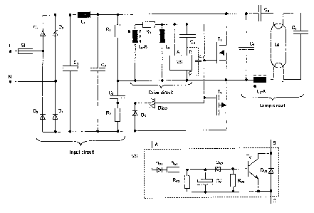
BRIEF DESCRIPTION OF THE DRAWING
Represented in more detail below is an exemplary
embodiment according to the invention which serves to
illustrate the various features according to the
invention. The individual features disclosed in this
case can also be essential to the invention in other
combinations as illustrated. As a precaution, it is
pointed out that the invention could be claimed not
only within the scope of product claims, but also
within the scope of method claims, and thus that the
preceding and following disclosure is therefore also to
be read and understood with regard to method features.
BEST MODE FOR CARRYING OUT THE INVENTION
The figure shows a circuit diagram of an exemplary
embodiment for an operating circuit according to the
invention.
In the drawing, La denotes a low-pressure discharge
lamp, it being illustrated diagrammatically that two
incandescent filaments are connected into the part of
the operating circuit denoted as lamp circuit in the
figure. The incandescent filaments are connected via a
capacitor C7, which serves as resonance capacitor. In
the case of conventional circuits for preheating the
electrodes, a parallel circuit composed of a further
capacitor and a PTC thermistor is connected in series
with the resonance capacitor C7, in order to ensure
that the electrodes are preheated in the way already
described. This further capacitor and the PTC
thermistor are no longer required in the invention.
' CA 02399793 2002-08-26
- 10 -
The~discharge lamp La is supplied as follows: a fuse Si
is connected to the mains input (domestic mains
voltage) denoted by L and N. Following this is a
rectifier comprising the diodes Dl to D4, the output of
which rectifier has a smoothing capacitor C1. L1 denotes
a filter inductor and CZ a capacitor; together, the two
assemblies form an interference suppressor.
There follows the actual oscillator circuit with two
switching transistors T1 and T2, more specifically
MOSFET transistors. The assemblies R1, Rz, C3, D5 and
the diac form a starting circuit which is known per se.
In the case of this starting circuit, after mains
voltage has been applied to the terminals L and N the
capacitor C3 is recharged until a breakdown voltage is
present at the diac and said voltage provides a first
drive pulse for the switching transistors T1 and TZ . In
the further operation, the connection of the capacitor
C3 prevents the latter from resupplying a drive pulse.
The mode of operation of the starting circuit is
immaterial for the present invention.
The discharge lamp La is connected via a resonance
inductance L3-A to the centre tap between the two
switching transistors T1 and T2, which form a half
bridge, and connected at the other electrode via a
decoupling capacitor C6 to the upper supply branch in
the figure, that is to say one of the two outer
terminals of the half bridge.
The resonance inductance L3-A, the decoupling capacitor
C6 and the resonance capacitor C7 form a series resonant
circuit. The capacitor CS serves merely to relieve the
switching transistors T1 and T2, and contributes to the
interference suppression.
The switching transistors are driven via the drive
circuit, thus denoted in th-e figure, whose component VS
' CA 02399793 2002-08-26
- 11 -
is expressly illustrated in the lower part of the
figure and is responsible for preheating the electrodes
of the discharge lamp La. In continuous operation, the
emitter-collector section of the transistor TV is
turned on in the preheating circuit VS such that the
two points B and C are connected. In this state, the
drive circuit forms an independent resonant circuit
with the inductance L2 and the capacitance C4. When, on
the other hand, the emitter-collector section of the
transistor T~ is open, the resonant circuit in the
drive circuit comprises only the inductance LZ together
with the transistor input capacitances of the switching
transistors T1 and Tz. If the transistor input
capacitances do not suffice for the functioning,
explained further below, of the resonant circuit in
this state, the auxiliary capacitor Cgb Illustrated by
dashes in the figure can be inserted, and forms a
suitable (comparatively small) total capacitance in
series connection with the capacitor C4.
In this exemplary embodiment, the control circuit is
provided only once and connected to the control
electrodes of both switching transistors T1 and T2. This
is possible because, as the graphical symbols in the
figure make plain, the switching transistors are
complementary ones.
It is also to be seen that a winding L3-B is connected
via the resistor R3 to the resonant circuit in the
drive circuit, this winding L3-B being coupled to the
already mentioned resonance inductance L3-A in the lamp
circuit. This can be a transformer (not saturating in
normal operation) here, but two inductances can also be
mounted efficiently close to one another as to produce
a magnetic coupling. The coupling serves for
synchronizing the oscillations of the drive circuit and
the remaining oscillator circuit, and for feeding
energy into the resonant circuit. The circuit diagram
shows that, specifically, the resonant circuit in the
CA 02399793 2002-08-26
- 12 -
drive circuit defines an independent frequency with
reference to the lamp circuit with the emitter-
collector sections of the switching transistors T1 and
T2. A system of two coupled oscillators is produced by
the coupling via the inductances L3-A and L3-B and the
control electrodes of the switching transistors T1 and
Tz. This is utilized for the purpose of firstly
preheating the discharge lamp La after starting
(starting pulse of the diac) by virtue of the fact that
the emitter-collector section of the transistor T~ in
the preheating circuit VS remains open, and thus the
resonant circuit composed of the inductance LZ and the
input capacitances of the switching transistors T1 and
Tz, or the overall capacitance CQ in series with C9b
oscillates at a somewhat higher frequency with
reference to the natural frequency of the series
resonant circuit in the lamp circuit. However, in this
case the frequency prescribed by the resonant circuit
is detuned upward with reference to the natural
frequency of the series resonant circuit only to the
extent that the oscillator circuit also oscillators to
a certain extent, that is to say energy is also fed
back into the resonant circuit via the transformer.
Because of the frequency detuning, no adequate voltage
rise occurs in the lamp circuit between the electrodes,
and so the discharge lamp La is not triggered. Instead,
a preheating current flows through the electrodes as a
consequence of the forced oscillation in the oscillator
circuit.
Moreover, if the transistor input capacitances of the
switching transistors T1 and T2 should, together with
the inductance LZ, define a natural frequency, already
close to ignition frequency, of the resonant circuit in
the drive circuit, then either the inductance LZ could
be varied, or an additional damping could be
undertaken.
If, now, a preheating time whose technical
CA 02399793 2002-08-26
- 13 -
implementation is yet to be considered in detail, has
expired, the emitter-collector section of the
transistor T~ is switched on, and so the frequency of
the resonant circuit in the drive circuit is determined
by the inductance LZ together with the capacitance C4.
This frequency is in the vicinity of the resonant
frequency of the remaining oscillator (that is to say
of the series resonant circuit of the lamp circuit
together with the switching paths of the switching
transistors T1 and TZ) .
As a consequence of the resonant increase, this
produces between the already preheated electrodes a
voltage sufficient to ignite the discharge lamp La, and
so the discharge lamp La is triggered. As soon as the
ignition has occurred, the discharge lamp La forms a
parallel current path to the resonance capacitor C7,
such that only relatively slight currents still flow
through the electrodes to the capacitor C~.
The switching operation of the transistor T~, which
firstly switches out the capacitance C9 and then
switches it in, is controlled in the following way: a
capacitor C~ entered in the detailed illustration of
the preheating circuit VS is recharged starting from a
point A via a diode D~,1 and a resistor Rvl until the sum
of the required base-emitter voltage and the
breakthrough voltage of a zener diode Dz,z is reached.
One side of the capacitor C~ is connected via this
zener diode D"2 to the control electrode (the base of
the bipolar transistor T~) , while the other side of the
capacitor C~ is connected to another terminal (the
emitter) of the transistor T~. As a result, the
capacitor voltage is applied to the emitter-base
junction such that the emitter-collector section of the
transistor T~ is turned on. However, as long as the
breakthrough voltage of the zener diode Lh,2 is not
reached the base and the emitter of the transistor T~
are short circuited via the resistor R~z such that the
CA 02399793 2002-08-26
- 14 -
emitter-collector section remains open. The diode
is, moreover, a freewheeling diode customary for
connecting bipolar transistors.
Moreover, connected in parallel with the capacitor C~
is a discharge resistor R~3 which, after the entire
operating circuit is switched off, discharges the
capacitor again in a very short time interval for the
use of the discharge lamp La, and thus.permits the
discharge lamp La to be switched on again briefly with
proper preheating. On the other hand, discharging of
the transistor T~ due to this resistor R~3 is slow
enough to design the discharging to be weak enough by
comparison with the charging operations by the diode D1,1
and the resistor R~l.
The resistor R~1 brakes the recharging of the capacitor
C~ and thereby serves to define the preheating time
together with the capacitance of the capacitor and the
breakdown voltage of the diode D~,2.
The resistor R~2 also serves to avoid excessively strong
functional relationships between scatter bands of
different individual transistors T~.
Overall, the operating circuit from the figure in
conjunction with the discharge lamp La should be an
integrated solution, that is to say, for example, a
compact fluorescent lamp with a ballast integrated in
the cap. However, the circuit can be applied just as
effectively to separate solutions in the case of which
a discharge lamp La can be connected with its
electrodes to corresponding terminals of the operating
circuit. Moreover, instead of the illustrated supply
via the mains voltage to be applied to the terminals L
N, it would also be possible, of course, to provide
another supply, for example from a battery, in which
case the rectifier could then be eliminated.