Note : Les descriptions sont présentées dans la langue officielle dans laquelle elles ont été soumises.
CA 02400513 2002-08-07
WO 01/59835 PCT/USO1/04208
SEMICONDUCTOR DEVICES
Field of the Invention
This invention relates generally to semiconductor
devices, and more specifically to compound semiconductor
devices and to the use of semiconductor devices, and
integrated circuits that include a monocrystalline
compound semiconductor material.
Background of the Invention
The vast majority of semiconductor discrete devices
and integrated circuits are fabricated from silicon, at
least in part because of the availability of inexpensive,
high quality monocrystalline silicon substrates. Other
semiconductor materials, such as the so called compound
semiconductor materials, have physical attributes,
including wider bandgap and/or higher mobility than
silicon, or direct bandgaps that makes these materials
advantageous for certain types of semiconductor devices.
Unfortunately, compound semiconductor materials are
generally much more expensive than silicon and are not
available in large wafers as is silicon. Gallium arsenide
(GaAs), the most readily available compound semiconductor
material, is available in wafers only up to about 150
millimeters (mm) in diameter. In contrast, silicon wafers
are available up to about 300 mm and are widely available
at 200 mm. The 150 mm GaAs wafers are many times more
expensive than are their silicon counterparts. Wafers of
other compound semiconductor materials are even less
available and are more expensive than GaAs.
Because of the desirable characteristics of compound
semiconductor materials, and because of their present
CA 02400513 2002-08-07
WO 01/59835 PCT/USO1/04208
2
generally high cost and low availability in bulk form, for
many years attempts have been made to grow thin films of
the compound semiconductor materials on a foreign
substrate. To achieve optimal characteristics of the
compound semiconductor material, however, a
monocrystalline film of high crystalline quality is
desired. Attempts have been made, for example, to grow
layers of a monocrystalline compound semiconductor
material on germanium, silicon, and various insulators.
These attempts have generally been unsuccessful because
lattice mismatches between the host crystal and the grown
crystal have caused the resulting thin film of compound
semiconductor material to be of low crystalline quality.
If a large area thin film of high quality
monocrystalline compound semiconductor material was
available at low cost, a variety of semiconductor devices
could advantageously be fabricated in that film at a low
cost compared to the cost of fabricating such devices on a
bulk wafer of compound semiconductor material or in an
epitaxial film of such material on a bulk wafer of
compound semiconductor material. In addition, if a thin
film of high quality monocrystalline compound
semiconductor material could be realized on a bulk wafer
such as a silicon wafer, an integrated device structure
could be achieved that took advantage of the best
properties of both the silicon and the compound
semiconductor material.
Accordingly, a need exists for a semiconductor device
that provides a high quality monocrystalline compound
semiconductor film over another monocrystalline material.
Brief Description of the Drawings
CA 02400513 2002-08-07
WO 01/59835 PCT/USO1/04208
3
The present invention is illustrated by way of
example and not limitation in the accompanying figures, in
which like references indicate similar elements, and in
which:
FIGS. 1, 2, 4, 5 illustrate schematically, in cross
section, device structures in accordance with various
embodiments of the invention;
FIG. 3 illustrates graphically the relationship
between maximum attainable film thickness and lattice
mismatch between a host crystal and a grown crystalline
overlayer;
FIG. 6 includes an illustration of a block diagram of
a portion of a communicating device;
FIGS. 7-11 include illustrations of cross-sectional
views of a portion of an integrated circuit that includes
a compound semiconductor portion, a bipolar portion, and
an MOS portion; and
FIGS. 12-18 includes illustrations of cross-sectional
views of a portion of another integrated circuit that
includes a semiconductor laser and an MOS transistor.
Skilled artisans will appreciate that elements in the
figures are illustrated for simplicity and clarity and
have not necessarily been drawn to scale. For example,
the dimensions of some of the elements in the figures may
be exaggerated relative to other elements to help to
improve understanding of embodiments of the present
invention.
Detailed Description of the Drawings
FIG. 1 illustrates schematically, in cross section, a
portion of a semiconductor structure 20 in accordance with
an embodiment of the invention. Semiconductor structure
20 includes a monocrystalline substrate 22, accommodating
buffer layer 24 comprising a monocrystalline material, and
CA 02400513 2002-08-07
WO 01/59835 PCT/USO1/04208
4
a layer 26 of a monocrystalline compound semiconductor
material. In this context, the term "monocrystalline"
shall have the meaning commonly used within the
semiconductor industry. The term shall refer to materials
that are a single crystal or that are substantially a
single crystal and shall include those materials having a
relatively small number of defects such as dislocations
and the like as are commonly found in substrates of
silicon or germanium or mixtures of silicon and germanium
and epitaxial layers of such materials commonly found in
the semiconductor industry.
In accordance with one embodiment of the invention,
structure 20 also includes an amorphous intermediate layer
28 positioned between substrate 22 and accommodating
buffer layer 24. Structure 20 may also include a template
layer 30 between the accommodating buffer layer and
compound semiconductor layer 26. As will be explained
more fully below, the template layer helps to initiate the
growth of the compound semiconductor layer on the
accommodating buffer layer. The amorphous intermediate
layer helps to relieve the strain in the accommodating
buffer layer and by doing so, aids in the growth of a high
crystalline quality accommodating buffer layer.
Substrate 22, in accordance with an embodiment of the
invention, is a monocrystalline semiconductor wafer,
preferably of large diameter. The wafer can be of a
material from Group IV of the periodic table, and
preferably a material from Group IVA. Examples of Group
IV semiconductor materials include silicon, germanium,
mixed silicon and germanium, mixed silicon and carbon,
mixed silicon, germanium and carbon, and the like.
Preferably substrate 22 is a wafer containing silicon or
germanium, and most preferably is a high quality
monocrystalline silicon wafer as used in the semiconductor
industry. Accommodating buffer layer 24 is preferably a
CA 02400513 2002-08-07
WO 01/59835 PCT/USO1/04208
monocrystalline oxide or nitride material epitaxially
grown on the underlying substrate. In accordance with one
embodiment of the invention, amorphous intermediate layer
28 is grown on substrate 22 at the interface between
5 substrate 22 and the growing accommodating buffer layer by
the oxidation of substrate 22 during the growth of layer
24. The amorphous intermediate layer serves to relieve
strain that might otherwise occur in the monocrystalline
accommodating buffer layer as a result of differences in
the lattice constants of the substrate and the buffer
layer. As used herein, lattice constants refers to the
distance between atoms of a cell measured in the plane of
the surface. If such strain is not relieved by the
amorphous intermediate layer, the strain may cause defects
in the crystalline structure of the accommodating buffer
layer. Defects in the crystalline.structure of the
accommodating buffer layer, in turn, would make it
difficult to achieve a high quality crystalline structure
in monocrystalline compound semiconductor layer 26.
Accommodating buffer layer 24 is preferably a
monocrystalline oxide or nitride material selected for its
crystalline compatibility with the underlying substrate
and with the overlying compound semiconductor material.
For example, the material could be an oxide or nitride
having a lattice structure matched to the substrate and to
the subsequently applied semiconductor material.
Materials that are suitable for the accommodating buffer
layer include metal oxides such as the alkaline earth
metal titanates, alkaline earth metal zirconates, alkaline
earth metal hafnates, alkaline earth metal tantalates,
alkaline earth metal ruthenates, alkaline earth metal
niobates, alkaline earth metal vanadates, alkaline earth
metal tin-based perovskites, lanthanum aluminate,
lanthanum scandium oxide, and gadolinium oxide.
Additionally, various nitrides such as gallium nitride,
CA 02400513 2002-08-07
WO 01/59835 PCT/USO1/04208
6
aluminum nitride, and boron nitride may also be used for
the accommodating buffer layer. Most of these materials
are insulators, although strontium ruthenate, for example,
is a conductor. Generally, these materials are metal
oxides or metal nitrides, and more particularly, these
metal oxide or nitrides typically include at least two
different metallic elements. In some specific
applications, the metal oxides or nitride may include
three or more different metallic elements.
Amorphous interface layer 28 is preferably an oxide
formed by the oxidation of the surface of substrate 22,.
and more preferably is composed of a silicon oxide. The
thickness of layer 28 is sufficient to relieve strain
attributed to mismatches between the lattice constants of
substrate 22 and accommodating buffer layer 24..
Typically, layer 28 has a thickness in the range of
approximately 0.5-5 nm.
The compound semiconductor material of layer 26 can
be selected, as needed for a particular semiconductor
structure, from any of the Group IIIA and VA elements
(III-V semiconductor compounds), mixed III-V compounds,
Group II(A or B) and VIA elements (II-VI semiconductor ,
compounds), and mixed II-VI compounds. Examples include
gallium arsenide (GaAs), gallium indium arsenide (GaInAs),
gallium aluminum arsenide (GaAlAs), indium phosphide
(InP), cadmium sulfide (CdS), cadmium mercury telluride
(CdHgTe), zinc selenide (ZnSe), zinc sulfur selenide
(ZnSSe), and the like. Suitable template materials
chemically bond to the surface of the accommodating buffer
layer.24 at selected sites and provide sites for the
nucleation of the epitaxial growth of the subsequent
compound semiconductor layer 26. Appropriate materials
for template 30 are discussed below.
FIG. 2 illustrates, in cross section, a portion of a
semiconductor structure 40 in accordance with a further
CA 02400513 2002-08-07
WO 01/59835 PCT/USO1/04208
7.
embodiment of the invention. Structure 40 is similar to
the previously described semiconductor structure 20 except
that an additional buffer layer 32 is positioned between
accommodating buffer layer 24 and layer of monocrystalline
compound semiconductor material 26. Specifically, the
additional buffer layer is positioned between the template
layer 30 and the overlying layer of compound semiconductor'
material. The additional buffer layer, formed of a
semiconductor or compound semiconductor material, serves
to provide a lattice compensation when the lattice
constant of the accommodating buffer layer cannot be
adequately matched to the overlying monocrystalline
compound semiconductor material layer.
The following non-limiting, illustrative examples
illustrate various combinations of materials useful in
structure 20 and structure 40 in accordance with various
alternative embodiments of the invention. These examples
are merely illustrative, and it is not intended that the
invention be limited to these illustrative examples.
Example 1
In accordance with one embodiment of the invention,
monocrystalline substrate 22 is a silicon substrate
oriented in the (100) direction. The silicon substrate
can be, for example, a silicon substrate as is commonly
used in making complementary metal oxide semiconductor
(CMOS) integrated circuits having a diameter of about 200-
300 mm. In accordance with this embodiment of the
invention, accommodating buffer layer 24 is a
monocrystalline layer of SrZBaI_ZTi03 where z ranges from 0
to 1 and the amorphous intermediate layer is a layer of
silicon oxide (SiOX) formed at the interface between the
silicon substrate and the accommodating buffer layer. The
value of z is selected to obtain one or more lattice
CA 02400513 2002-08-07
WO 01/59835 PCT/USO1/04208
8
constants closely matched to corresponding lattice
constants of the subsequently formed layer 26. The
accommodating buffer layer can have a thickness of about 2
to about 100 nanometers (nm) and preferably has a
thickness of about 10 nm. In general, it is desired to
have an accommodating buffer layer thick enough to isolate
the compound semiconductor layer from the substrate to
obtain the desired electrical and optical properties.
Layers thicker than 100 nm usually provide little
additional benefit while increasing cost unnecessarily;
however, thicker layers may be fabricated if needed. The
amorphous intermediate layer of silicon oxide can have a
thickness of about 0.5-5 nm, and preferably a thickness of
about 1.5-2.5 nm.
In accordance with this embodiment of the invention,
compound semiconductor material layer 26 is a layer of
gallium arsenide (GaAs) or aluminum gallium arsenide
(AlGaAs) having a thickness of about 1 nm to about 100
micrometers (gym) and preferably a thickness of about 0.5
~.m to 10 Vim. The thickness generally depends on the
application for which the layer is being prepared. To-
facilitate the epitaxial growth of the gallium arsenide or
aluminum gallium arsenide on the monocrystalline oxide, a
template layer is formed by capping the oxide layer. The
template layer is preferably 1-10 monolayers of Ti-As, Sr-
O-As, Sr-Ga-O, or Sr-A1-O. By way of a preferred example,
1-2 monolayers of Ti-As or Sr-Ga-O have been shown to
successfully grow GaAs layers.
Example 2
In accordance with a further embodiment of the
invention, monocrystalline substrate 22 is a silicon
substrate as described above. The accommodating buffer
layer is a monocrystalline oxide of strontium or barium
CA 02400513 2002-08-07
WO 01/59835 PCT/USO1/04208
9
zirconate or hafnate in a cubic or orthorhombic phase with
an amorphous intermediate layer of silicon oxide formed at
the interface between the silicon substrate and the
accommodating buffer layer. The accommodating buffer
layer can have a thickness of about 2-100 nm and
preferably has a thickness of at least 5 nm to ensure
adequate crystalline and surface quality and is formed of
a monocrystalline SrZr03, BaZr03, SrHf03, BaSn03 or BaHf03.
For example, a monocrystalline oxide layer of BaZr03 can
grow at a temperature of about 700 degrees C. The lattice
structure of the resulting crystalline oxide exhibits a 45
degree rotation with respect to the substrate silicon
lattice structure.
An accommodating buffer layer formed of these
zirconate or hafnate materials is suitable for the growth
of compound semiconductor materials in the indium
phosphide (InP) system. The compound semiconductor
material can be, for example, indium phosphide (InP) or
indium gallium arsenide (InGaAs) having a thickness of
about 1.0 nm to 10 Vim. A suitable template for this
structure is 1-10 monolayers of zirconium-arsenic (Zr-As),
zirconium-phosphorus (Zr-P), hafnium-arsenic (Hf-As),
hafnium-phosphorus (Hf-P), strontium-oxygen-arsenic (Sr-O-
As), strontium-oxygen-phosphorus (Sr-O-P), barium-oxygen-
arsenic (Ba-O-As), indium-strontium-oxygen (In-Sr-O), or
barium-oxygen-phosphorus (Ba-O-P), and preferably 1-2
monolayers of one of these materials. By way of an
example, for a barium zirconate accommodating buffer
layer, the surface is terminated with 1-2 monolayers of
zirconium followed by deposition of 1-2 monolayers of
arsenic to form a Zr-As template. A monocrystalline layer
of the compound semiconductor material from the indium
phosphide system is then grown on the template layer. The
resulting lattice structure of the compound semiconductor
material exhibits a 45 degree rotation with respect to the
CA 02400513 2002-08-07
WO 01/59835 PCT/USO1/04208
accommodating buffer layer lattice structure and a lattice
mismatch to (100) InP of less than 2.50, and preferably
less than about 1.0%.
5 Example 3
In accordance with a further embodiment of the
invention, a structure is provided that is suitable for
the growth of an epitaxial film of a II-VI material
10 overlying a silicon substrate. The substrate is
preferably a silicon wafer as described above. A suitable
accommodating buffer layer material is SrXBa,_XTi03, where x
ranges from 0 to 1, having a thickness of about 2-100 nm
and preferably a thickness of about 5-15 nm. The II-VI
compound semiconductor material can be, for example, zinc
selenide (ZnSe) or zinc sulfur selenide (ZnSSe). A
suitable template for this material system includes 1-10
monolayers of zinc-oxygen (Zn-O) followed by 1-2
monolayers of an excess of zinc followed by the
selenidation of zinc on the surface. Alternatively, a
template can be, for example, strontium-sulfur (Sr-S)
followed by the ZnSeS.
Example 4
This embodiment of the invention is an example of
structure 40 illustrated in FIG. 2. Substrate 22,
monocrystalline oxide layer 24, and monocrystalline
compound semiconductor material layer 26 can be similar to
those described in example 1. In addition, an additional
buffer layer 32 serves to alleviate any strains that might
result from a mismatch of the crystal lattice of the
accommodating buffer layer and the lattice of the
monocrystalline semiconductor material. Buffer layer 32
can be a gallium arsenide phosphide (GaAsXPl_X) or indium
CA 02400513 2002-08-07
WO 01/59835 PCT/USO1/04208
11
gallium phosphide ( InyGal_yP) strain compensated
superlattice. In the gallium arsenide phosphide
superlattice the value of x ranges from 0 to 1, and in the
indium gallium phosphide superlattice the value of y
ranges from 0 to 1. By so varying the value of x or y, as
the case may be, the lattice constant is varied from
bottom to top across the superlattice to create a match
between lattice constants of the underlying oxide and the
overlying compound semiconductor material. The
superlattice can have a thickness of about 50-500 nm and
preferably has a thickness of about 200-100 nm. The
template for this structure can be the same of that
described in example 1. Alternatively, the buffer layer
can be a layer of monocrystalline germanium having a
thickness of 1-50 rim and preferably having a thickness of
about 2-20 nm. In using a germanium buffer layer, a
template layer of either germanium-strontium (Ge-Sr) or
germanium-titanium (Ge-Ti) having a thickness of about one
monolayer can be used. The formation of the oxide layer
is capped with either a monolayer of strontium or a
monolayer of titanium to act as a nucleating site for the
subsequent deposition of the monocrystalline germanium.
The monolayer of strontium or titanium provides a
nucleating site to which the first monolayer of germanium
can bond.
Example 5
This example also illustrates materials useful in a
structure 40 as illustrated in FIG. 2. Substrate material
22, accommodating buffer layer 24, monocrystalline
compound semiconductor material layer 26 and template
layer 30 can be the same as those described above in
example 2. In addition, a buffer layer 32 is inserted
between the accommodating buffer layer,and the overlying
CA 02400513 2002-08-07
WO 01/59835 PCT/USO1/04208
12
monocrystalline compound semiconductor material layer.
The buffer layer, a further monocrystalline semiconductor
material, can be, for example, a graded layer of indium
gallium arsenide (InGaAs) in which the indium composition
varies from 0 to about 47%. The buffer layer preferably
has a thickness of about 10-30 nm. Varying the
composition of the buffer layer from GaAs to InGaAs serves
to provide a lattice match between the underlying
monocrystalline oxide material and the overlying layer of
monocrystalline compound semiconductor material. Such a
buffer layer is especially advantageous if there is a
lattice mismatch between accommodating buffer layer 24 and
monocrystalline compound semiconductor material layer 26.
Referring again to FIGS. 1 and 2, substrate 22 is a
monocrystalline substrate such as a monocrystalline
silicon substrate. The crystalline structure of the
monocrystalline substrate is characterized by a lattice
constant and by a lattice orientation. In similar manner,
accommodating buffer layer 24 is also a monocrystalline
material and the lattice of that monocrystalline material
is characterized by a lattice constant and a crystal
orientation. The lattice constants of the accommodating
buffer layer and the monocrystalline substrate must be
closely matched or, alternatively, must be such that upon
rotation of one crystal orientation with respect to the
other crystal orientation, a substantial match in lattice
constants is achieved. In this context the terms
"substantially equal" and "substantially matched" mean
that there is sufficient similarity between the lattice
constants to permit the growth of a high quality
crystalline layer on the underlying layer.
FIG. 3 illustrates graphically the relationship of
the achievable thickness of a grown crystal layer of high
crystalline quality as a function of the mismatch between
the, lattice constants of the host crystal and the grown
CA 02400513 2002-08-07
WO 01/59835 PCT/USO1/04208
13
crystal. Curve 42 illustrates the boundary of high
crystalline quality material. The area to the right of
curve 42 represents layers that tend to be
polycrystalline. With no lattice mismatch, it is
theoretically possible to grow an infinitely thick, high
quality epitaxial layer on the host crystal. As the
mismatch in lattice constants increases, the thickness of
achievable, high quality crystalline layer decreases
rapidly. As a reference point, for example, if the lattice
constants between the host crystal and the grown layer are
mismatched by more than about 20, monocrystalline
epitaxial layers in excess of about 20 nm cannot be
achieved.
In accordance with one embodiment of the invention,
substrate 22 is a (100) or (111) oriented monocrystalline
silicon wafer and accommodating buffer layer 24 is a layer
of strontium barium titanate. Substantial matching of
lattice constants between these two materials is achieved
by rotating the crystal orientation of the titanate
material by 45° with respect to the crystal orientation of
the silicon substrate wafer. The inclusion in the
structure of amorphous interface layer 24, a silicon oxide
layer in this example, serves to reduce strain in the
titanate monocrystalline layer that might result from any
mismatch in the lattice constants of the host silicon
wafer and the grown titanate layer. As a result, in
accordance with an embodiment of the invention, a high
quality, thick, monocrystalline titanate layer is
achievable.
Still referring to FIGS. 1 and 2, layer 26 is a layer
of epitaxially grown monocrystalline compound
semiconductor material and that crystalline material is
also characterized by a crystal lattice constant and a
crystal orientation. To achieve high crystalline quality
in this epitaxially grown layer, the accommodating buffer
CA 02400513 2002-08-07
WO 01/59835 PCT/USO1/04208
14
layer must be of high crystalline quality. In addition,
in order to achieve high crystalline quality in layer 26,
substantial matching between the crystal lattice constant
of the host crystal, in this case, the monocrystalline
accommodating buffer layer, and the grown crystal is
desired. With properly selected materials this
substantial matching of lattice constants is achieved as a
result of rotation of the crystal orientation of the grown
crystal with respect to the orientation of the host
crystal. If the grown crystal is gallium arsenide,
aluminum gallium arsenide, zinc selenide, or zinc sulfur
selenide and the accommodating buffer layer is
monocrystalline SrXBal_XTi03, substantial matching of
crystal lattice constants of the two materials is
achieved, wherein the crystal orientation of the grown
layer is rotated by 45° with respect to the orientation of
the host monocrystalline oxide. Similarly, if the host
material is a strontium or barium zirconate or a strontium
or barium hafnate or barium tin oxide and the compound
semiconductor layer is indium phosphide or gallium indium
arsenide or aluminum indium arsenide, substantial matching
of crystal lattice constants can be achieved by rotating
the orientation of the grown crystal layer by 45° with
respect to the host oxide crystal. In some instances, a
crystalline semiconductor buffer layer between the host
oxide and the grown compound semiconductor layer can be
used to reduce strain in the grown monocrystalline
compound semiconductor layer that might result from small
differences in lattice constants. Better crystalline
quality in the grown monocrystalline compound
semiconductor layer can thereby be achieved.
The following example illustrates a process, in
accordance with one embodiment of the invention, for
fabricating a semiconductor structure such as the
structures depicted in FIGS. 1 and 2. The process starts
CA 02400513 2002-08-07
WO 01/59835 PCT/USO1/04208
by providing a monocrystalline semiconductor substrate
comprising silicon or germanium. In accordance with a
preferred embodiment of the invention, the semiconductor
substrate is a silicon wafer having a (100) orientation.
5 The substrate is preferably oriented on axis or, at most,
about 0.5° off axis. At least a portion of the
semiconductor substrate has a bare surface, although other
portions of the substrate, as described below, may
encompass other structures. The term "bare" in this
10 context means that the surface in the portion of the
substrate has been cleaned to remove any oxides,
contaminants, or other foreign material. As is well
known, bare silicon is highly reactive and readily forms a
native oxide. The term "bare" is intended to encompass
15 such a native oxide. A thin silicon oxide may also be
intentionally grown on the semiconductor substrate,
although such a grown oxide is not essential to the
process in accordance with the invention. In order to
epitaxially grow a monocrystalline oxide layer overlying
the monocrystalline substrate, the native oxide layer must
first be removed to expose the crystalline structure of
the underlying substrate. The following process is
preferably carried out by molecular beam epitaxy (MBE).
The native oxide can be removed by first thermally
depositing a thin layer of strontium in an MBE apparatus.
The substrate is then heated to a temperature of about
750° C to cause the strontium to react with the native
silicon oxide layer. The strontium serves to reduce the
silicon oxide to leave a silicon oxide-free surface. The
resultant surface, which exhibits an ordered 2x1
structure, includes strontium, oxygen, and silicon. The
ordered 2x1 structure forms a template for the ordered
growth of an overlying layer of a monocrystalline oxide.
The template provides the necessary chemical and physical
CA 02400513 2002-08-07
WO 01/59835 PCT/USO1/04208
16
properties to nucleate the crystalline growth of an
overlying layer.
In accordance with an alternate embodiment of the
invention, the native silicon oxide can be converted and
the substrate surface can be prepared for the growth of a
monocrystalline oxide layer by depositing strontium oxide
onto the substrate surface by MBE at a low temperature and
by subsequently heating the structure to a temperature of
about 750°C. At this temperature a solid state reaction
takes place between the strontium oxide and the native
silicon oxide causing the reduction of the native silicon
oxide and leaving an ordered 2x1 structure with strontium,
oxygen, and silicon remaining on the substrate surface.
Again, this forms a template for the subsequent growth of
an ordered monocrystalline oxide layer.
Following the removal of the silicon oxide from the
surface of the substrate, in accordance with one
embodiment of the invention,.the substrate is cooled to a
temperature in the range of about 400-600°C and a layer of
strontium titanate is grown on the template layer by
molecular beam epitaxy. The MBE process is initiated by
opening shutters in the MBE apparatus to expose strontium,
titanium and oxygen sources. The ratio of strontium and
titanium is approximately 1:1. The partial pressure of
oxygen is initially set at a minimum value to grow
stochiometric strontium titanate at a growth rate of about
0.3-0.5 nm per minute. After initiating growth of the
strontium titanate, the partial pressure of oxygen is
increased above the initial minimum value. The
overpressure of oxygen causes the growth of an amorphous
silicon oxide layer at the interface between the
underlying substrate and the growing strontium titanate
layer. The growth of the silicon oxide layer results from
the diffusion of oxygen through the growing strontium
titanate layer to the interface where the oxygen reacts
CA 02400513 2002-08-07
WO 01/59835 PCT/USO1/04208
17
with silicon at the surface of the underlying substrate.
The strontium titanate grows as an ordered monocrystal
with the crystalline orientation rotated by 45° with
respect to the ordered 2x1 crystalline structure of the
underlying substrate. Strain that otherwise might exist
in the strontium titanate layer because of the small
mismatch in lattice constant between the silicon substrate
and the growing crystal is relieved in the amorphous
silicon oxide intermediate layer.
After the strontium titanate layer has been grown to
the desired thickness, the monocrystalline strontium
titanate is capped by a template layer that is conducive
to the subsequent growth of an epitaxial layer of a
desired compound semiconductor material. For the
subsequent growth of a layer of gallium arsenide, the MBE
growth of the strontium titanate monocrystalline layer can
be capped by terminating the growth with 1-2 monolayers of
titanium, 1-2 monolayers of titanium-oxygen or with 1-2
monolayers of strontium-oxygen. Following the formation
of this capping layer, arsenic is deposited to form a Ti-
As bond, a Ti-O-As bond or a Sr-O-As. Any of these form an
appropriate template for deposition and formation of a
gallium arsenide monocrystalline layer. Following the
formation of the template, gallium is introduced to the
reaction with the arsenic and gallium arsenide forms.
Alternatively, gallium can be deposited on the capping
layer to form a Sr-O-Ga bond, and arsenic is introduced
with the gallium to form the GaAs.
The structure illustrated in FIG. 2 can be formed by
the process discussed above with the addition of an
additional buffer layer deposition step. The buffer layer
is formed overlying the template layer before the
deposition of the monocrystalline compound semiconductor
layer. If the buffer layer is a compound semiconductor
superlattice, such a.superlattice can be deposited, by MBE
CA 02400513 2002-08-07
WO 01/59835 PCT/USO1/04208
18
for example, on the template described above. If instead
the buffer layer is a layer of germanium, the process
above is modified to cap the strontium titanate
monocrystalline layer with a final layer of either
strontium or titanium and then by depositing germanium to
react with the strontium or titanium. The germanium
buffer layer can then be deposited directly on this
template.
The process described above illustrates a process for
forming a semiconductor structure including a silicon
substrate, a monocrystalline strontium titanate
accommodating buffer layer, and a monocrystalline gallium
arsenide compound semiconductor layer by the process of
molecular beam epitaxy. The process can also be carried
out by the process of chemical vapor deposition (CVD),
metal organic chemical vapor deposition (MOCVD), migration
enhanced epitaxy (MEE), atomic layer epitaxy (ALE), or the
like. Further, by a similar process, other
monocrystalline accommodating buffer layers such as
alkaline earth metal titanates, zirconates, hafnates,
tantalates, vanadates, ruthenates, and niobates, alkaline
earth metal tin-based perovskites, lanthanum aluminate,
lanthanum scandium oxide, and gadolinium oxide can also be
grown. Further, by a similar process such as MBE, other
III-V and II-VI monocrystalline compound semiconductor
layers can be deposited overlying the monocrystalline
oxide accommodating buffer layer.
Each of the variations of compound semiconductor
materials and monocrystalline oxide accommodating buffer
layer uses an appropriate template for initiating the
grown of the compound semiconductor layer. For example,
if the accommodating buffer layer is alkaline earth metal
zirconate, the oxide can be capped by a thin layer of
zirconium. The deposition of zirconium can be followed by
the deposition of arsenic or phosphorus to react with the
CA 02400513 2002-08-07
WO 01/59835 PCT/USO1/04208
19
zirconium as a precursor to depositing indium gallium
arsenide, indium aluminum arsenide, or indium phosphide
respectively. Similarly, if the monocrystalline oxide
accommodating buffer layer is an alkaline earth metal
hafnate, the oxide layer can be capped by a thin layer of
hafnium. The deposition of hafnium is followed by the
deposition of arsenic or phosphorous to react with the
hafnium as a precursor to the growth of an indium gallium
arsenide, indium aluminum arsenide, or indium phosphide
layer, respectively. In a similar manner, strontium
titanate can be capped with a layer of strontium or
strontium and oxygen and barium titanate can be capped
with a layer of barium or barium and oxygen. Each of
these depositions can be followed by the deposition of
arsenic or phosphorus to react with the capping material
to form a template for the deposition of a compound
semiconductor material layer comprising indium gallium
arsenide, indium aluminum arsenide, or indium phosphide.
FIG. 4 illustrates schematically, in cross section, a
device structure 50 in accordance with a further
embodiment of the invention. Device structure 50 includes
a monocrystalline semiconductor substrate 52, preferably a
monocrystalline silicon wafer. Monocrystalline
semiconductor substrate 52 includes two regions, 53 and
54. An electrical semiconductor component generally
indicated by the dashed line 56 is formed in region 53.
Electrical component 56 can be a resistor, a capacitor, an
active semiconductor component such as a diode or a
transistor or an integrated circuit such as a CMOS
integrated circuit. For example, electrical semiconductor
component 56 can be a CMOS integrated circuit configured
to perform digital signal processing or another function
for which silicon integrated circuits are well suited.
The electrical semiconductor component in region 53 can be
formed by conventional semiconductor processing as well
CA 02400513 2002-08-07
WO 01/59835 PCT/USO1/04208
known and widely practiced in the semiconductor industry.
A layer of insulating material 58 such as a layer of
silicon dioxide or the like may overlie electrical
semiconductor component 56.
5 Insulating material 58 and any other layers that may
have been formed or deposited during the processing of
semiconductor component 56 in region 53 are removed from
the surface of region 54 to provide a bare silicon surface
in that region. As is well known, bare silicon surfaces
10 are highly reactive and a native silicon oxide layer can
quickly form on the bare surface. A layer of barium or
barium and oxygen is deposited onto the native oxide layer
on the surface of region 54 and is reacted with the
oxidized surface to form a first template layer (not
15 shown). In accordance with one embodiment of the
invention a monocrystalline oxide layer 60 is formed
overlying the template layer by a process of molecular
beam epitaxy. Reactants including barium, titanium and
oxygen are deposited onto the template layer to form the
20 monocrystalline oxide layer. Initially during the
deposition the partial pressure of oxygen is kept near the
minimum necessary to fully react with the barium and
titanium to form monocrystalline barium titanate layer 60.
The partial pressure of oxygen is then increased to
provide an overpressure of oxygen and to allow oxygen to
diffuse through the growing monocrystalline oxide layer.
The oxygen diffusing through the barium titanate reacts
with silicon at the surface of region 54 to form an
amorphous layer 62 of silicon oxide on the second region
and at the interface between the silicon substrate and the
monocrystalline oxide.
In accordance with an embodiment of the invention,
the step of depositing monocrystalline oxide layer 60 is
terminated by depositing a second template layer 64, which
can be 1-10 monolayers of titanium, barium, barium and
CA 02400513 2002-08-07
WO 01/59835 PCT/USO1/04208
21
oxygen, or titanium and oxygen. A layer 66 of a
monocrystalline compound semiconductor material is then
deposited overlying the second template layer by a process
of molecular beam epitaxy. The deposition of layer 66 is
initiated by depositing a layer of arsenic onto the
template. This initial step is followed by depositing
gallium and arsenic to form monocrystalline gallium
arsenide. Alternatively, strontium can be substituted for
barium in the above example.
In accordance with a further embodiment of the
invention, a semiconductor component, generally indicated
by a dashed line 68 is formed in compound semiconductor
layer 66. Semiconductor component 68 can be formed by
processing steps conventionally used in the fabrication of
gallium arsenide or other III-V compound semiconductor
material devices. Semiconductor component 68 can be any
active or passive component, and preferably is a
semiconductor laser, light emitting diode, photodetector,
heterojunction bipolar transistor (HBT), high frequency
MESFET, or other component that utilizes and takes
advantage of the physical properties of compound
semiconductor materials. A metallic conductor
schematically indicated by the line 70 can be formed to
electrically couple device 68 and device 56, thus
implementing an integrated device that includes at least
one component formed in the silicon substrate and one
device formed in the monocrystalline compound
semiconductor material layer. Although illustrative
structure 50 has been described as a structure formed on a
silicon substrate 52 and having a barium (or strontium)
titanate layer 60 and a gallium arsenide layer 66, similar
devices can be fabricated using other substrates,
monocrystalline oxide layers and other compound
semiconductor layers as described elsewhere in this
disclosure.
CA 02400513 2002-08-07
WO 01/59835 PCT/USO1/04208
22
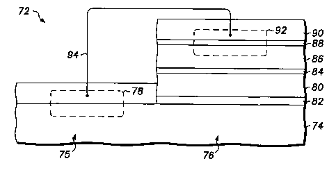
FIG. 5 illustrates a semiconductor structure 72 in
accordance with a further embodiment of the invention.
Structure 72 includes a monocrystalline semiconductor
substrate 74 such as a monocrystalline silicon wafer that
includes a region 75 and a region 76. An electrical
component schematically illustrated by the dashed line 78
is formed in region 75 using conventional silicon device
processing techniques commonly used in the semiconductor
industry. Using process steps similar to those described
above, a monocrystalline oxide layer 80 and an
intermediate amorphous silicon oxide layer 82 are formed
overlying region 76 of substrate 74. A template layer 84
and subsequently a monocrystalline semiconductor layer 86
are formed overlying monocrystalline oxide layer 80. In
accordance with a further embodiment of the invention, an
additional monocrystalline oxide layer 88 is formed
overlying layer 86 by process steps similar to those used
to form layer 80, and an additional monocrystalline
semiconductor layer 90 is formed overlying monocrystalline
oxide layer 88 by process steps similar to those used to
form layer 86. In accordance with one embodiment of the
invention, at least one of layers 86 and 90 are formed
from a compound semiconductor material.
A semiconductor component generally indicated by a
dashed line 92 is formed at least partially in
monocrystalline semiconductor layer 86. In accordance
with one embodiment of the invention, semiconductor
component 92 may include a field effect transistor having
a gate dielectric formed, in part, by monocrystalline
oxide layer 88. In addition, monocrystalline
semiconductor layer 92 can be used to implement the gate
electrode of that field effect transistor. In accordance
with one embodiment of the invention, monocrystalline
semiconductor layer 86 is formed from a group III-V
compound and semiconductor component 92 is a radio
CA 02400513 2002-08-07
WO 01/59835 PCT/USO1/04208
23
frequency amplifier that takes advantage of the high
mobility characteristic of group III-V component
materials. In accordance with yet a further embodiment of
the invention, an electrical interconnection schematically
illustrated by the line 94 electrically interconnects
component 78 and component 92. Structure.72 thus
integrates components that take advantage of the unique
properties of the two monocrystalline semiconductor
materials.
By way of more specific examples, other integrated
circuits and systems are illustrated in FIGS. 6-18. FIG.
6 includes a simplified block diagram illustrating a
portion of a communicating device 100 having a signal
transceiving means 101, an integrated circuit 102, an
output unit 103, and an input unit 104. Examples of the
signal transceiving means include an antenna, a modem, or
any other means by which information or data can be sent
either to or from an external unit. As used herein,
transceiving is used to denote that the signal
transceiving means may be capable of only receiving, only
transmitting, or both receiving and transmitting signals
from or to the communicating device. The output unit 103
can include a display, a monitor, a speaker, or the like.
The input unit can include a microphone, a keyboard, or
the like. Note that in alternative embodiments the output
unit 103 and input unit 104 could be replaced by a single
unit such as a memory, or the like. The memory can
include random access memory or nonvolatile memory, such
as a hard disk, a flash memory card or module, or the
like.
An integrated circuit is generally a combination of
at least two circuit elements (e. g., transistors, diodes,
resistors, capacitors, and the like) inseparably
associated on or within a continuous substrate. The
integrated circuit 102 includes a compound semiconductor
CA 02400513 2002-08-07
WO 01/59835 PCT/USO1/04208
24
portion 1022, a bipolar portion 1024, and an MOS portion
1026. The compound semiconductor portion 1022 includes
electrical components that are formed at least partially
within a compound semiconductor material. Transistors and
other electrical components within the compound
semiconductor portion 1022 are capable of processing
signals at radio frequencies of at least approximately 0.8
GHz. In other embodiments, the signals could be at lower
or higher frequencies. For example, some materials, such
as indium gallium arsenide, are capable of processing
signals at radio frequency signals at approximately 27
GHz.
The compound semiconductor portion 1022 further
includes a duplexer 10222, a radio frequency-to-baseband
converter 10224 (demodulating means or demodulating
circuit), baseband-to-radio frequency converter 10226
(modulating means or modulating circuit), a power
amplifier 10228, and an isolator 10229. The bipolar
portion 1024 and the MOS portion 1026 typically are formed
in a Group IV semiconductive material. The bipolar
portion 1024 includes a receiving amplifier 10242, an
analog-to-digital converter 10244, a digital-to-analog
converter 10246, and a transmitting amplifier 10248. The
MOS portion 1026 includes a digital signal processing
means 10262. An example of such means includes any one of
the commonly available DSP cores available in the market,
such as the Motorola DSP 566xx (from Motorola,
Incorporated of Schaumburg, Illinois) and Texas
Instruments TMS 320C54x (from Texas Instruments of Dallas,
Texas) families of digital signal processors. This
digital signal processing means 10262 typically includes
complementary MOS (CMOS) transistors and analog-to-digital
and digital-to-analog converters. Clearly, other
electrical components are present in the integrated
circuit 102.
CA 02400513 2002-08-07
WO 01/59835 PCT/USO1/04208
In one mode of operation, the communicating device
100 receives a signal from an antenna, which is part of
the signal transceiving means 101. The signal passes
through the duplexer 10227 to the radio frequency-to-
5 baseband converter 10224. The analog data or other
information is amplified by receiving amplifier 10224 and
transmitted to the digital signal processing means 10262.
After the digital signal processing means 10262 has
processed the information or other data, the processed
10 information or other data is transmitted to the output
unit 103. If the communicating device is a pager, the
output unit can be a display. If the communicating device
is a cellular telephone, the output unit 103 can include a
speaker, a display, or both.
15 Data or other information can be sent through the
communicating device 100 in the opposite direction. The
data or other information will come in through the input
unit 104. In a cellular telephone, this could include a
microphone or a keypad. The information or other data is
20 then processed using the digital signal processing means
10262. After processing, the signal is then converted
using the digital-to-analog converter 10246. The
converted signal is amplified by the transmitting
amplifier 10248. The amplified signal is modulated by the
25 baseband-to-radio frequency converter 10226 and further
amplified by power amplifier 10228. The amplified RF
signal passes through the isolator 10229 and duplexer
10222 to the antenna.
Prior art embodiments of the communicating device 100
would have at least two separate integrated circuits: one
for the compound semiconductor portion 1022 and one for
the MOS portion 1026. The bipolar portion 1024 may be on
the same integrated circuit as the MOS portion 1026 or
could be on still another integrated circuit. With an
embodiment of the present invention, all three portions
CA 02400513 2002-08-07
WO 01/59835 PCT/USO1/04208
26
can now be formed within a single integrated circuit.
Because all of the transistors can reside on a single
integrated circuit, the communicating device can be
greatly miniaturized and allow for greater portability of
a communicating device.
Attention is now directed to a method for forming
exemplary portions of the integrated circuit 102 as~
illustrated in FIGs. 7-11. In FIG. 7, a p-type doped,
monocrystalline silicon substrate 110 is provided having a
compound semiconductor portion 1022, a bipolar portion
1024, and an MOS portion 1026. Hlithin the bipolar
portion, the monocrystalline silicon substrate is doped to
form an N' buried region 1102. A lightly p-type doped
epitaxial monocrystalline silicon layer 1104 is then
formed over the buried region 1102 and the substrate 110.
A doping step is then performed to create a lightly n-type
doped drift region 1117 above the N' buried region 1102.
The doping step converts the dopant type of the lightly p-
type epitaxial layer within a section of the bipolar
region 1024 to a lightly n-type monocrystalline silicon
region. A field isolation region 1106 is then formed
between the bipolar portion 1024 and the MOS portion 1026.
A gate dielectric layer 1110 is formed over a portion of
the epitaxial layer 1104 within MOS portion 1026, and the
gate electrode 1112 is then formed over the gate
dielectric layer 1110. Sidewall spacers 1115 are formed
along vertical sides of the gate electrode 1112 and gate
dielectric layer 1110.
A p-type dopant is introduced into the drift region
1117 to form an active or intrinsic base region 1114. An
n-type, deep collector region 1108 is then formed within
the bipolar portion 1024 to allow electrical connection to
the buried region 1102. Selective n-type doping is
performed to form N+ doped regions 1116 and the emitter.
region 1120. N+ doped regions 1116 are formed within layer
CA 02400513 2002-08-07
WO 01/59835 PCT/USO1/04208
27
1104 along adjacent sides of the gate electrode 1112 and
are source, drain, or source/drain regions for the MOS
transistor. The N' doped regions 1116 and emitter region
1120 have a doping concentration of at least 1E19 atoms
per cubic centimeter to allow ohmic contacts to be formed.
A p-type doped region is formed to create the inactive or
extrinsic base region 1118 which is a P+ doped region
(doping concentration of at least 1E19 atoms per cubic
centimeter).
In the embodiment described, several processing steps
have been performed but are not illustrated or further
described, such as the formation of well regions,
threshold adjusting implants, channel punchthrough
prevention implants, field punchthrough prevention
implants, as well as a variety of masking layers. The
formation of the device up to this point in the process is
performed using conventional steps. As illustrated, a
standard N-channel MOS transistor has been formed within
the MOS region 1026, and a vertical NPN bipolar transistor
has been formed within the bipolar portion 1024. As of
this point, no circuitry has been formed within the
compound semiconductor portion 1022.
All of the layers that have been formed during the
processing of the bipolar and MOS portions of the
integrated circuit are now removed from the surface of
compound semiconductor portion 1022. A bare silicon
surface is thus provided for the subsequent processing of
this portion, for example in the manner set forth above.
An accommodating buffer layer 124 is then formed over
the substrate 110 as illustrated in FIG. 8. The
accommodating buffer layer will form as a monocrystalline
layer over the properly prepared (i.e., having the
appropriate template layer) bare silicon surface in
portion 1022. The portion of layer 124 that forms over
portions 1024 and 1026, however, may be polycrystalline or
CA 02400513 2002-08-07
WO 01/59835 PCT/USO1/04208
28
amorphous because it is formed over a material that is not
monocrystalline, and therefore, does not nucleate
monocrystalline growth. The accommodating buffer layer
124 typically is a monocrystalline metal oxide or nitride
layer and typically has a thickness in a range of
approximately 2-100 nanometers. In one particular
embodiment, the accommodating buffer layer is
approximately 5-15 nm thick. During the formation of the
accommodating buffer layer, an amorphous intermediate
layer 122 is formed along the uppermost silicon surfaces
of the integrated circuit 102. This amorphous
intermediate layer 122 typically includes an oxide of
silicon and has a thickness and range of approximately 1-5
nm. In one particular embodiment, the thickness is
approximately 2 nm. Following the formation of the
accommodating buffer layer 124 and the amorphous
intermediate layer 122, a template layer 126 is then
formed and has a thickness in a range of approximately one
to ten monolayers of a material. In one particular
embodiment, the material includes titanium-arsenic,
strontium-oxygen-arsenic, or other similar materials as
previously described with respect to FIGS. 1-5.
A monocrystalline compound semiconductor layer 132 is
then epitaxially grown overlying the monocrystalline
portion of accommodating buffer layer 124 as shown in FIG.
9. The portion of layer 132 that is grown over portions
of layer 124 that are not monocrystalline may be
polycrystalline or amorphous. The monocrystalline
compound semiconductor layer can be formed by a number of
methods and typically includes a material such as gallium
arsenide, aluminum gallium arsenide, indium phosphide, or
other compounds semiconductor materials as previously
mentioned. The thickness of the layer is in a range of
approximately 1-5,000 nm, and more preferably 100-500 rim.
In this particular embodiment, each of the elements within
CA 02400513 2002-08-07
WO 01/59835 PCT/USO1/04208
29
the template layer are also present in the accommodating
buffer layer 124, the monocrystalline compound
semiconductor material 132, or both. Therefore, the
delineation between the template layer 126 and its two
immediately adjacent layers disappears during processing.
Therefore, when a transmission electron microscopy (TEM)
photograph is taken, an interface between the
accommodating buffer layer 124 and the monocrystalline
compound semiconductor layer 132 is seen.
At this point in time, sections of the compound
semiconductor layer 132 and the accommodating buffer layer
124 are removed from portions overlying the bipolar
portion 1024 and the MOS portion 1026 as shown in FIG. 10.
After the section is removed, an insulating layer 142 is
then formed over the substrate 110. The insulating layer
142 can include a number of materials such as oxides,
nitrides, oxynitrides, low-k dielectrics, or the like. As
used herein, low-k is a material having a dielectric
constant no higher than approximately 3.5. After the
insulating layer 142 has been deposited, it is then
polished, removing portions of the insulating layer 142
that overlie monocrystalline compound semiconductor layer
132.
A transistor 144 is then formed within the
monocrystalline compound semiconductor portion 1022. A
gate electrode 148 is then formed on the monocrystalline
compound semiconductor layer 132. Doped regions 146 are
then formed within the monocrystalline compound
semiconductor layer 132. In this embodiment, the
transistor 144 is a metal-semiconductor field-effect
transistor (MESFET). If the MESFET is an n-type MESFET,
the doped regions 146 and monocrystalline compound
semiconductor layer 132 are also n-type doped. If a p-
type MESFET were to be formed, then the doped regions 146
and monocrystalline compound semiconductor layer 132 would
CA 02400513 2002-08-07
WO 01/59835 PCT/USO1/04208
have just the opposite doping type. The heavier doped (N+)
regions 146 allow ohmic contacts to be made to the
monocrystalline compound semiconductor layer 132. At this
point in time, the active devices within the integrated
5 circuit have been formed. This particular embodiment
includes an n-type MESFET, a vertical NPN bipolar
transistor, and a planar n-channel MOS transistor. Many
other types of transistors, including P-channel MOS
transistors, p-type vertical bipolar transistors, p-type
10 MESFETs, and combinations of vertical and planar
transistors, can be used. Also, other electrical
components, such as resistors, capacitors, diodes, and the
like, may be formed in one or more of the portions 1022,
1024, and 1026.
15 Processing continues to form a substantially
completed integrated circuit 102 as illustrated in FIG.
11. An insulating layer 152 is formed over the substrate
110. The insulating layer 152 may include an etch-stop or
polish-stop region that is not illustrated in the FIG. 11.
20 A second insulating layer 154 is then formed over the
first insulating layer 152. Portions of layers 154, 152,
142, 124, and 122 are removed to define contact openings
where the devices are to be interconnected. Interconnect
trenches are formed within insulating layer 154 to provide
25 the lateral connections between the contacts. As
illustrated in FIG. 11, interconnect 1562 connects a
source or drain region of the n-type MESFET within portion
1022 to the deep collector region 1108 of the NPN
transistor within the bipolar portion 1024. The emitter
30 region 1120 of the NPN transistor is connected to one of
the doped regions 1116 of the n-channel MOS transistor
within the MOS portion 1026. The other doped region 1116
is electrically connected to other portions of the
integrated circuit that are not shown.
CA 02400513 2002-08-07
WO 01/59835 PCT/USO1/04208
31
A passivation layer 156 is formed over the
interconnects 1562, 1564, and 1566 and insulating layer
154. Other electrical connections are made to the
transistors as illustrated as well as to other electrical
or electronic components within the integrated circuit 102
but are not illustrated in the figures. Further,
additional insulating layers and interconnects may be
formed as necessary to form the proper interconnections
between the various components within the integrated
circuit 102.
As can be seen from the previous embodiment, active
devices for both compound semiconductor and Group IV
semiconductor materials can be integrated into a single
integrated circuit. Because there is some difficulty in
incorporating both bipolar transistors and MOS transistors
within a same integrated circuit, it may be possible to
move some of the components within bipolar portion into
the compound semiconductor portion 1022 or the MOS portion
1024. More specifically, turning to the embodiment as
described with respect to FIG. 6, the amplifiers 10248 and
10242 may be moved over to the compound semiconductor
portion 1022, and the converters 10244 and 10246 can be
moved over into the MOS portion 1026. Therefore, the
requirement of special fabricating steps solely used for
making a bipolar transistor can be eliminated. Therefore,
there would only be a compound semiconductor portion and a
MOS portion to the integrated circuit.
In still another embodiment, an integrated circuit
can be formed such that it includes an optical laser in a
compound semiconductor portion and an optical interconnect
(waveguide) to an MOS transistor within a Group IV
semiconductor region of the same integrated circuit.
FIGS. 12-18 include illustrations of one embodiment.
FIG. 12 includes an illustration of a cross-section
view of a portion of an integrated circuit 160 that
CA 02400513 2002-08-07
WO 01/59835 PCT/USO1/04208
32
includes a monocrystalline silicon wafer 161. An
amorphous intermediate layer 162 and an accommodating
buffer layer 164, similar to those previously described,
have been formed over wafer 161. In this specific
embodiment, the layers needed to form the optical laser
will be formed first, followed by the layers needed for
the MOS transistor. In FIG. 12, the lower mirror layer
166 includes alternating layers of compound semiconductor
materials. For example, the first, third, and fifth films
within the optical laser may include a material such as
gallium arsenide, and the second, fourth, and sixth films
within the lower mirror layer 166 may include aluminum
gallium arsenide or vice versa. Layer 168 includes the
active region that will be used for photon generation.
Upper mirror layer 170 is formed in a similar manner to
the lower mirror layer 166 and includes alternating films
of compound semiconductor materials. In one particular
embodiment, the upper mirror layer 170 may be p-type doped
compound semiconductor materials, and the lower mirror
layer 166 may be n-type doped compound semiconductor
materials.
Another accommodating buffer layer 172, similar to
the accommodating buffer layer 164, is formed over the
upper mirror layer 170. In an alternative embodiment, the
accommodating buffer layers 164 and 172 may include
different materials. However, their function is
essentially the same in that each is used for making a
transition between a compound semiconductor layer and a
monocrystalline Group IV semiconductor layer. A
monocrystalline Group IV semiconductor layer 174 is formed
over the accommodating buffer layer 172. In one
particular embodiment, the monocrystalline Group IV
semiconductor layer 174 includes germanium, silicon
germanium, silicon germanium carbide, or the like.
CA 02400513 2002-08-07
WO 01/59835 PCT/USO1/04208
33
In FIG. 13, the MOS portion is processed to form
electrical components within this upper monocrystalline
Group IV semiconductor layer 174. As illustrated in FIG.
13, a field isolation region 171 is formed from a portion
of layer 174. A gate dielectric layer 173 is formed over
the layer 174, and a gate electrode 175 is formed over the
gate dielectric layer 173. Doped regions 177 are source,
drain, or source/drain regions for the transistor 181, as
shown. Sidewall spacers 179 are formed adjacent to the
vertical sides of the gate electrode 175. Other
components can be made within at least a part of layer
174. These other components include other transistors (n-
channel or p-channel), capacitors, transistors, diodes,
and the like.
A monocrystalline Group IV semiconductor layer is
epitaxially grown over one of the doped regions 177. An
upper portion 184 is P+ doped, and a lower portion 182
remains substantially intrinsic (undoped) as illustrated
in FIG. 13. The layer can be formed using a selective
epitaxial process. In one embodiment,. an insulating layer
(not shown) is formed over the transistor 181 and the
field isolation region 171. The insulating layer is
patterned to define an opening that exposes one of the
doped regions 177. At least initially, the selective
epitaxial layer is formed without dopants. The entire
selective epitaxial layer may be intrinsic, or a p-type
dopant can be added near the end of the formation of the
selective epitaxial layer. If the selective epitaxial
layer is intrinsic, as formed, a doping step may be formed
by implantation or by furnace doping. Regardless how the
P+ upper portion 184 is formed, the insulating layer is
then removed to form the resulting structure shown in FIG.
13.
The next set of steps is performed to define the
optical laser 180 as illustrated in FIG. 14. The field
CA 02400513 2002-08-07
WO 01/59835 PCT/USO1/04208
34
isolation region 171 and the accommodating buffer layer
172 are removed over the compound semiconductor portion of
the integrated circuit. Additional steps are performed to
define the upper mirror layer 170 and active layer 168 of
the optical laser 180.. The sides of the upper mirror
layer 170 and active layer 168 are substantially
coterminous.
Contacts 186 and 188 are formed for making electrical
contact to the upper mirror layer 170 and the lower mirror
layer 166, respectively, as shown in FIG. 14. Contact 186
has an annular shape to allow light (photons) to pass out
of the upper mirror layer 170 into a subsequently formed
optical waveguide.
An insulating layer 190 is then formed and patterned
to define optical openings extending to the contact layer
186 and one of the doped regions 177 as shown in FIG. 15.
The insulating material can be any number of different
materials, including an oxide, nitride, oxynitride, low-k
dielectric, or any combination thereof. After defining
the openings 192, a higher refractive index material 202
is then formed within the openings to fill them and to
deposit the layer over the insulating layer 190 as
illustrated in FIG. 16. With respect to the higher
refractive index material 202, "higher" is in relation to
the material of the insulating layer 190 (i.e., material
202 has a higher refractive index compared to the
insulating layer 190). Optionally, a relatively thin
lower refractive index film (not shown) could be formed
before forming the higher refractive index material 202.
A hard mask layer 204 is then formed over the high
refractive index layer 202. Portions of the hard mask
layer 204, and high refractive index layer 202 are removed
from portions overlying the opening and to areas closer to
the sides of FIG. 16.
CA 02400513 2002-08-07
WO 01/59835 PCT/USO1/04208
The balance of the formation of the optical
waveguide, which is an optical interconnect, is completed
as illustrated in FIG. 17. A deposition procedure
(possibly a dep-etch process) is performed to effectively
5 create sidewalls sections 212. In this embodiment, the
sidewall sections 212 are made of the same material as
material 202. The hard mask layer 204 is then removed,
and a low refractive index layer 214 (low relative to
material 202 and layer 212) is formed over the higher
10 refractive index material 212 and 202 and exposed portions
of the insulating layer 190. The dash lines in FIG. 17
illustrate the border between the high refractive index
materials 202 and 212. This designation is used to
identify that both are made of the same material but are
15 formed at different times.
Processing is continued to form a substantially
completed integrated circuit as illustrated in FIG. 18. A
passivation layer 220 is then formed over the optical
laser 180 and MOSFET transistor 181. Although not shown,
20 other electrical or optical connections are made to the
components within the integrated circuit but are not
illustrated in FIG. 18. These interconnects can include
other optical waveguides or may include metallic
interconnects.
25 In other embodiments, other types of lasers can be
formed. For example, another type of laser can emit light
(photons) horizontally instead of vertically. If light is
emitted horizontally, the MOSFET transistor could be
formed within the substrate 161, and the optical waveguide
30 would be reconfigured, so that the laser is properly
coupled (optically connected) to the transistor. In one
specific embodiment, the optical waveguide can include at
least a portion of the accommodating buffer layer. Other
configurations are possible.
CA 02400513 2002-08-07
WO 01/59835 PCT/USO1/04208
36
Clearly, these embodiments of integrated circuits
having compound semiconductor portions and Group IV
semiconductor portions, are meant to illustrate
embodiments of the present invention and not limit the
present invention. There are multiplicity of other
combinations and other embodiments of the present
invention. For example, the compound semiconductor
portion may include light emitting diodes, photodetectors,
diodes, or the like, and the Group IV semiconductor can
include digital logic, memory arrays, and most structures
that can be formed in conventional MOS integrated
circuits. By using embodiments of the present invention,
it is now simpler to integrate devices that work better in
compound semiconductor materials with other components
that work better in Group IV semiconductor materials.
This allows a device to be shrunk, the manufacturing costs
to decrease, and yield and reliability to increase.
Although not illustrated, a monocrystalline Group IV
wafer can be used in forming only compound semiconductor
electrical components over the wafer. In this manner, the
wafer is essentially a "handle" wafer used during the
fabrication of the compound semiconductor electrical
components within a monocrystalline compound semiconductor
layer overlying the wafer. Therefore, electrical
components can be formed within III-V or II-VI
semiconductor materials over a wafer of at least
approximately 200 millimeters in diameter and possibly at
least approximately 300 millimeters.
By the use of this type of substrate, a relatively
inexpensive "handle" wafer. overcomes the fragile nature of
the compound semiconductor wafers by placing them over a
relatively more durable and easy to fabricate base
material. Therefore, an integrated circuit can be formed
such that all electrical components, and particularly all
active electronic devices, can be formed within the
CA 02400513 2002-08-07
WO 01/59835 PCT/USO1/04208
37
compound semiconductor material even though the substrate
itself may include a Group IV semiconductor material.
Fabrication costs for compound semiconductor device should
decrease because larger substrates can be processed more
economically and more readily compared to the relatively
smaller and more fragile, conventional compound
semiconductor wafers.
In the foregoing specification, the invention has
been described with reference to specific embodiments.
However, one of ordinary skill in the art appreciates that
various modifications and changes can be made without
departing from the scope of the present invention as set
forth in the claims below. Accordingly, the specification
and figures are to be regarded in an illustrative rather
than a restrictive sense, and all such modifications are
intended to be included within the scope of present
invention.
Benefits, other advantages, and solutions to problems
have been described above with regard to specific
embodiments. However, the benefits, advantages, solutions
to problems, and any elements) that may cause any
benefit, advantage, or solution to occur or become more
pronounced are not to be construed as a critical,
required, or essential feature or element of any or all
the claims. As used herein, the terms "comprises,"
"comprising," or any other variation thereof, are intended
to cover a non-exclusive inclusion, such that a process,
method, article, or apparatus that comprises a list of
elements does not include only those elements but may
include other elements not expressly listed or inherent to
such process, method, article, or apparatus.