Note : Les descriptions sont présentées dans la langue officielle dans laquelle elles ont été soumises.
CA 02401539 2009-09-18
79628-33
I
METHOD AND DEVICE FOR ACTIVE IMPEDANCE MATCHING
By Ramon Hernandez-Marti, Austin, Texas
BACKGROUND
The invention relates generally to transmission lines and, more particularly,
to
adjusting the terminating and driving impedance of a transmission line to
match the
characteristic impedance of the transmission line.
It is well known to skilled practitioners in the electrical arts that if a
source
impedance is matched to a complex conjugate of a load impedance, maximum power
transfer between the source and the load is achieved. However, it is difficult
to match the
imaginary part of the complex impedance and half of the power is lost in the
matched
source impedance when using passive components for impedance matching.
Although
this is a characteristic of many electrical circuits, it may take on greater
significance
where transmission lines are considered. With transmission lines, the primary
objective
is to avoid reflections in the transmission line, so the characteristic
impedance is
assumed to be resistive.
Transmission lines, where the transmission line length is large with respect
to the
wavelength of the lowest transmission frequency, are commonly used for
transmission
of data between two or more locations. It is well known in the art of
transmission lines,
and particularly transmission lines for transmitting information at high data
rates, that in
order to maximize the efficiency of information transfer with minimum loss and
dispersion effects, the terminating impedance of a receiver and the driving
impedance of
a transmitter must match the characteristic impedance Zo of the transmission
line over
CA 02401539 2002-08-27
WO 01/65691 PCT/US01/05580
2
the frequency range of interest. That is, it is desirable to maintain a
uniform
characteristic impedance Z0 along the length of the signal carrying line. Any
mismatch
in the characteristic impedance across interconnect interfaces will cause
reflection of the
signal at the interface, resulting in losses and distortion of the signal in
the form of
attenuation, echo and cross-talk. Furthermore, multiple reflections from
multiple
interfaces only compound the deleterious affect on the information-carrying
signal. The
classical solution to the impedance matching problem involves attempting to
match the
distributed-parameter impedance of the transmission line with lumped-parameter
impedances of resistor, capacitor and inductor circuit elements.
Wide band communication channels, like ADSL modulation over telephone
conventional lines or other wideband modulation schemes, require matching of
line
impedances that are complex, where amplitude and phase are dependent on
frequency.
Telephone subscriber loops with bridged taps present impedance variations at
the
receiver end that are difficult to match using simple circuits. Furthermore,
the
impedances variations may change from loop to loop, making it impossible to
design a
matching circuit using generic discrete circuit components. The use of full-
duplex
techniques, where bi-directional transmission is conducted concurrently only
further
complicates the difficulty of matching interface impedances to the
characteristic
impedance of the transmission line.
There have been a number of different approaches to solving the characteristic
impedance matching problem. In the most simple and rudimentary form, fixed
resistor
elements are connected across the transmission line interfaces to match the
interface
impedance with the characteristic impedance of the transmission line. More
complex
impedance matching circuits using combinations of resistor and capacitor
elements are
CA 02401539 2002-08-27
WO 01/65691 PCT/USOI/05580
3
often found connected to transmission lines. Impedance matching circuits using
passive
components may dissipate half of the available power at the transmitter,
oftentimes
reducing its dynamic range by half. Although power is seldom a major
consideration on
a standard data transmission line, loss in dynamic range can result in
excessive signal
clipping with high peak to average ratios that are typical of Quadrature
Amplitude
Modulated signals and Discrete Multi-Tone signals, used in many modern data
transmission systems.
One of the oldest and widely used approaches to match a transmitter-receiver
to a
transmission line is a hybrid circuit that makes use of two transformers and a
balance
impedance network ZL that, when matched to the characteristic impedance Z0 of
the
transmission line, results in very high isolation between transmitter and
receiver circuits.
This circuit provides a line termination that matches the characteristic
impedance of the
line and results in no reduction in dynamic range. However, only half the
power
delivered by the transmitter is sent to the transmission line, the other half
being wasted
on the balancing impedance network ZL. In addition to loss of transmitted
power, the
balancing impedance network ZL cannot perfectly match a line with bridged taps
or
multiple interfaces. It is impractical to add switching circuits to adapt the
impedance to
different lines, where each line has a different configuration of taps or
interfaces along
the length of the line. Furthermore, this hybrid circuit makes use of multiple
magnetic
circuits that have inherent non-linear characteristics that produce
distortion, which
adversely affects signals with high peak to average ratios. These transformers
also
exhibit parasitic capacitance and leakage inductance that may impair circuit
operation
and reduce useful bandwidth.
CA 02401539 2002-08-27
WO 01/65691 PCT/USO1/05580
4
Another approach that has received increased interest is the use of a
differential
driver circuit having two outputs, where each output is connected through an
impedance
matching resistor to each of the two terminals, respectively, of the primary
winding of a
transformer. The secondary winding of the transformer is connected to the
transmission
line. However, not only is half of the transmitter power dissipated in the two
impedance
matching resistors, but half of the signal amplitude is also dropped across
these resistors.
This results in reducing the dynamic range of the signal at the transmitter by
one-half
and reducing the maximum power available to drive the transmission line by one-
fourth.
The transformer provides for scaling the line impedance to compensate for this
reduction
and for generating enough peak voltage without excessive clipping. Two
amplifiers,
each connected across a terminating resistor receive the signal on the
transmission line.
This circuit may only perform better than the hybrid circuit described above
in the high
frequency range, where the line impedance will be mostly resistive in nature.
Although
more complex networks may replace these terminating resistors, the resultant
configuration would also suffer from the same limitations as the hybrid
circuit described
above, namely low power efficiency and reduced dynamic range.
All of these solutions assume that the characteristic impedance of the
transmission line is fixed and known, and therefore terminated accordingly.
These
solutions result in reduced power available to the transmission line, reduced
dynamic
range of the signal, and losses and distortion in the signal. Although more
pronounced
with transmission lines, these problems apply to many electrical circuits.
For the foregoing reasons, it is desirable to have a method and device for
driving
and receiving signals on a transmission line that does not exhibit loss of the
available
transmitter power to drive the line, does not suffer from a reduction in
dynamic signal
CA 02401539 2009-09-18
79628-33
range, and dynamically matches the driving and terminating impedance at the
interfaces to
the characteristic impedance of the transmission line.
SUMMARY
According to one broad aspect, the present invention provides a device for
5 active impedance matching, the device comprising: a. a voltage driver having
an output
connected to a load; b. means for detecting an output current from the voltage
driver to the
load, the means for detecting an output current comprising a transformer
having a primary
winding in series with the output current; c. means for scaling the detected
output current by
a scaling value; and d. means for subtracting a value representing the scaled
detected
output current from an input signal of the voltage driver.
According to another broad aspect, the present invention provides a method
for active impedance matching, the method comprising: a. connecting an output
of a
voltage driver to a load; b. detecting an output current from the voltage
driver to the load,
the detecting comprising connecting a primary winding of a transformer in
series with the
output current; c. scaling the detected output current by a scaling value; and
d. subtracting
a value representing the scaled detected output current from an input signal
of the voltage
driver.
According to still another broad aspect, the present invention provides a
method for active impedance matching, the method comprising: a. connecting an
output of
a voltage driver to a load; b. detecting an output current value from the
voltage driver to the
load, the detecting comprising connecting a primary winding of a transformer
in series with
the output current; c. connecting the detected output current to an analog-to-
digital
converter; d. converting the detected output current value to a digital
representation by the
analog-to-digital converter; e. connecting the digital representation of the
output current at
an output of the analog-to-digital converter to an input of a digital signal
processor;
f. connecting a digital representation of an input signal to another input of
the digital signal
processor; g. executing a program in the digital signal processor, wherein the
program
comprises the steps of scaling the output current value and subtracting the
scaled output
current value from the digital representation of the input signal; h.
providing a digital
representation output from the digital signal processor to a digital-to-analog
converter; and
i. connecting an output of the digital-to-analog converter to an input of the
voltage driver.
CA 02401539 2009-09-18
79628-33
5a
The present invention is directed to a method and device for driving a load
with
active impedance matching that satisfies these needs. The present invention is
particularly suitable for providing a method and device for driving and
receiving signals
on a transmission line that does not exhibit loss of the available transmitter
power to
drive the line, does not suffer from a reduction in dynamic signal range, and
dynamically
matches the transmission line interface driving and terminating impedance to
the
characteristic impedance of the transmission line.
In a voltage driver version of the present invention, a means is provided for
sensing the current provided to a load by a voltage source, and the magnitude
of the
voltage source is automatically adjusted by negatively feeding back a voltage
to an input
that represents a scaled value of the sensed current multiplied by an
impedance that
matches the load impedance. The result is a voltage source having an effective
internal
impedance that matches the load impedance, but yet maintains full dynamic
signal range
without a loss of transmitted power to the load.
In a current driver version of the present invention, a means is provided for
sensing the voltage provided to a load by a current source, and the magnitude
of the
current source is automatically adjusted by negatively feeding back a current
to an input
that represents a scaled value of the sensed voltage divided by an impedance
that
matches the load impedance. The result is a current source having an effective
internal
CA 02401539 2009-09-18
79628-33
6
impedance that matches the load impedance, but yet maintains full dynamic
signal range
without a loss of transmitted power to the load.
Although the present method and device is applicable to many electrical
circuits,
its application is particularly suitable to transmission lines.
A device having features of the present invention is a device with active
impedance matching for driving a load that comprises a voltage driver having
an output
connected to a load, means for detecting an output current from the voltage
driver to the
load, means for scaling the detected output current by a scaling value, and
means for
subtracting a value representing the scaled detected output current from an
input signal
of the voltage driver. The means for scaling the detected output current may
be a
multiplier having an input comprising the detected output current and another
input
comprising the scaling value, an output of the multiplier representing the
scaled output
current. In some embodiments, the scaling value is a value representing a load
impedance to be matched. The means for scaling the detected output current may
be an
amplifier having an input comprising the detected output current and a gain
equal to the
scaling value, an output of the amplifier representing the scaled output
current. The
means for detecting an output current may be a transformer having a primary
winding in
series with the output current. The means for detecting an output current may
be a
resistor in series with the output current and an amplifier with inputs
connected to
terminals of the resistor. The means for subtracting may be a summing junction
of an
operational amplifier. The load may be a transmission line. The scaling value
may be a
characteristic impedance of the transmission line. The means for scaling and
the means
for subtracting may comprise a digital signal processor.
CA 02401539 2002-08-27
WO 01/65691 PCT/USO1/05580
7
In an alternative embodiment of the present invention, a device with active
impedance matching for driving a load comprises a current driver having an
output
connected to a load, means for detecting an output voltage from the current
driver to the
load, means for scaling the detected output voltage by a scaling value, and
means for
subtracting a value representing the scaled detected output voltage from an
input signal
of the current driver. The means for scaling the detected output voltage may
be a
multiplier having an input comprising the detected output voltage and another
input
comprising the scaling value, an output of the multiplier representing the
scaled output
voltage. The scaling value may be a value representing a load impedance to be
matched.
The means for scaling the detected output voltage may be an amplifier having
an input
comprising the detected output voltage and a gain equal to the scaling value,
an output of
the amplifier representing the scaled output voltage. The means for detecting
an output
voltage may be an amplifier with inputs connected to the outputs of the
current driver.
The means for detecting an output voltage may be a transformer with primary
terminals
connected to the outputs of the current driver. The means for subtracting may
be a
summing junction of an operational amplifier. The load may be a transmission
line. The
scaling value may be a characteristic impedance of the transmission line. The
means for
scaling and the means for subtracting may comprise a digital signal processor.
In another alternative embodiment of the present invention, a method for
driving
a load with active impedance matching, comprises connecting an output of a
voltage
driver to a load, detecting an output current from the voltage driver to the
load, scaling
the detected output current by a scaling value, and subtracting a value
representing the
scaled detected output current from an input signal of the voltage driver.
Scaling the
detected output current may comprise multiplying the detected output current
by the
CA 02401539 2002-08-27
WO 01/65691 PCT/USO1/05580
8
scaling value, an output of the multiplication representing the scaled output
current. The
scaling value may be a value representing a load impedance to be matched. The
detected
output current may comprise amplifying the detected output current by the
scaling value
for obtaining a value representing the scaled output current. Detecting an
output current
may comprise connecting a primary winding of a transformer in series with the
output
current. Detecting an output current may comprise connecting a resistor in
series with
the output current and connecting inputs of an amplifier to terminals of the
resistor.
Subtracting may comprise summing currents into a summing junction of an
operational
amplifier. The load may be a transmission line. The scaling value may be a
characteristic
impedance of the transmission line. Scaling and subtracting may comprise
processing
instructions of a digital signal processor.
In another alternative embodiment of the present invention, a method for
driving
a load with active impedance matching comprises connecting an output of a
current
driver to a load, detecting an output voltage from the current driver to the
load, scaling
the detected output voltage by a scaling value, and subtracting a value
representing the
scaled detected output voltage from an input signal of the current driver.
Scaling the
detected output voltage may comprise multiplying the detected output voltage
by the
scaling value, an output of the multiplication representing the scaled output
voltage. The
scaling value may be a value representing a load impedance to be matched.
Scaling the
detected output voltage may comprise amplifying the detected output voltage by
the
scaling value for obtaining a value representing the scaled output voltage.
Detecting an
output voltage may comprise connecting inputs of an amplifier to outputs of
the current
driver. Detecting an output voltage may comprise connecting a primary winding
of a
transformer to the outputs of the current driver. Subtracting may comprise
summing
CA 02401539 2002-08-27
WO 01/65691 PCT/USOI/05580
9
currents into a summing junction of an operational amplifier. The load may be
a
transmission line. The scaling value may be a characteristic impedance of the
transmission line. Scaling and subtracting may comprise processing
instructions of a
digital signal processor.
In another alternative embodiment of the present invention, a method for
driving
a load with active impedance matching comprises connecting an output of a
voltage
driver to a load, detecting an output current value from the voltage driver to
the load,
connecting the detected output current to an analog-to-digital converter,
converting the
detected output current value to a digital representation by the analog-to-
digital
converter, connecting the digital representation of the output current at an
output of the
analog-to-digital converter to an input of a digital signal processor,
connecting a digital
representation of an input signal to another input of the digital signal
processor,
executing a program in the digital signal processor, providing an digital
representation
output from the digital signal processor to a digital-to-analog converter, and
connecting
an output of the digital-to-analog converter to an input of the voltage
driver. The
method may further comprise interposing an anti-aliasing low-pass filter
between the
detected current output and the analog-to-digital converter. The method may
further
comprise interposing an interpolation low-pass filter between the output of
the digital-to-
analog converter and the input of the voltage driver. The step of connecting a
digital
representation of an input signal may comprise connecting an input signal to
another
input of the voltage driver. The step of executing a program in the digital
signal
processor may further comprise executing an initialization routine, reading an
input
voltage value, associating a time value with the input voltage value,
adjusting the time
value with a time domain filter delay, reading an output current value from
the analog-
CA 02401539 2002-08-27
WO 01/65691 PCT/USO1/05580
to-digital converter, applying the output current value to the time domain
filter,
subtracting the filtered output current value from the adjusted input voltage
value,
outputting the result of the subtraction to a digital-to-analog converter,
repeating steps b.
through h. if the program is not terminated, and ending the process if the
program is
5 terminated.
BRIEF DESCRIPTION OF THE DRAWINGS
These and other features, aspects, and advantages of the present invention
will
become understood with regard to the following description, appended claims,
and
10 accompanying drawings where:
FIG. 1A shows a half duplex configuration of a transmitter/receiver circuit;
FIG. 1B shows a full duplex configuration of a transmitter/receiver circuit;
FIG. 2A shows a Thevenin equivalent of a voltage transmitter circuit;
FIG. 2B shows an equivalent circuit of the circuit shown in FIG. 2A;
FIG. 3A shows a Norton equivalent of a current transmitter circuit;
FIG. 3B shows an equivalent circuit of the circuit shown in FIG. 3A;
FIG. 4 shows a block diagram of a voltage transmitter circuit;
FIG. 5 shows a block diagram of a current transmitter circuit;
FIG. 6A shows a circuit diagram of an a voltage transmitter using an inductive
sensor;
FIG. 6B shows a circuit diagram of a voltage transmitter using a resistive
sensor;
FIG. 7 shows a circuit diagram of a DSP implementation of a voltage
transmitter;
FIG. 8A shows a flow diagram of a program executed in the DSP of FIG. 7; and
FIG. 8B shows a flow diagram of an initialization routine.
CA 02401539 2002-08-27
WO 01/65691 PCT/USO1/05580
11
DETAILED DESCRIPTION
Turning now to FIG. 1A, FIG. 1A shows a half duplex configuration 10 of
transmitter/receiver circuit connected to a transmission line 140. This
configuration is
well known to skilled practitioners in the relevant art. In the half duplex
configuration of
FIG IA, a transmit input signal 112 is connected to an input of a differential
transmitter
102. An output of the transmitter is connected to a switch 1'06. A receive
output signal
114 is provided by an output of a differential receiver 104. An input of the
receiver 104
is connected to the switch 106. A transmission line signal 108, 110 is
connected to the
switch 106 such that the when the switch 106 is in position A, the
transmission line
signal 108, 110 is connected to the output of the transmitter 102, for
transmitting a
transmission line signal 108, 110. Alternatively, when the switch is in
position B, the
transmission line signal 108, 110 is connected to the input of the receiver
104, for
receiving a transmission line signal 108, 110. Although the switch 106 is
depicted as an
electromechanical device, skilled practitioners would recognize that a
semiconductor
device would normally provide this function for half duplex operation. In half
duplex
operation, a transmission line 140 is transmitting signals in one direction at
a time.
Turning now to FIG. 1B, FIG. lB shows a full duplex configuration 12 of
transmitter/receiver circuit connected to a transmission line 140. This
configuration is
also well known to skilled practitioners in the relevant art. In the half
duplex
configuration of FIG 1 B, a transmit input signal 112 is connected to an input
of a
differential transmitter 102. An output of the transmitter is connected to a
transmission
line signal 108, 110 through one port 128 of a hybrid coil or four-to-two wire
converter
126. A receive output signal 114 is provided by an output of a differential
receiver 104.
CA 02401539 2002-08-27
WO 01/65691 PCT/USO1/05580
12
An input of the receiver 104 is connected the transmission line signal 108,
110 through
another port 130 of the hybrid coil or four-to-two wire converter 126. In this
full duplex
configuration 12, the transmission line 140 may transmit signals in both
directions
simultaneously, the directional coupling and line termination being performed
by the
hybrid coil or four-to-two wire converter 126.
The subsequent descriptions of embodiments of the present invention pertain to
the transmitter 102 of FIG. IA and FIG. lB. Skilled practitioners will
recognize that
embodiments of the present invention may be used with a receiver 104 in either
a half
duplex configuration of FIG. lA or the full duplex configuration of FIG. 1B,
eliminating
the need for the switch 106 or the hybrid coil or four-to-two wire converter.
Turning now to FIG. 2A and FIG. 2B, FIG. 2A shows a Thevenin equivalent
circuit 20 of a voltage transmitter circuit and FIG. 2B shows an equivalent
circuit 22 of
the circuit 20 shown in FIG. 2A. In FIG. 2A, a voltage generator V. 202
represents a
Thevenin equivalent open circuit voltage source and an impedance Z. 204
represents a
Thevenin equivalent impedance. The circuit has an output voltage Vo 208 and an
output
current Io 206 connected to a load impedance ZL 240. By measuring the output
current Io
206 and negatively feeding it back with an appropriate gain required to
synthesize the
impedance Zg 204, the equivalent circuit 22 shown in FIG. 2B is formed. FIG.
2B
comprises a voltage generator 222 having a value of
Vo=Vg - Zglo
that provides the output voltage Vo 208 and the output current Io 206
connected to a load
impedance ZL 240. Note that Vo 208 and Io 206 are the same in FIG. 2A and FIG.
2B. If
the value of Vg is set to zero (short-circuit) and a current generator of
unity value is
connected to the outputs of the circuits shown in both FIG. 2A and FIG. 2B,
the value of
CA 02401539 2002-08-27
WO 01/65691 PCT/USOI/05580
13
the voltage Vo = Zg is the same in both circuits. This example illustrates the
principle of
operation of one of the embodiments of the present invention. That is, in a
voltage
transmitter circuit, the source impedance Zg 204 may be matched to a load
impedance ZL
240 by measuring the output current from the circuit and negatively feeding
back a
scaled part of the output current determined by the value of the load
impedance ZL 240.
In this manner, maximum power transfer may be achieved by setting Zg 204 = ZL
240
without power loss in Zg 204.
Turning now to FIG. 3A and FIG. 3B, FIG. 3A shows a Norton equivalent circuit
30 of a current transmitter circuit and FIG. 3B shows an equivalent circuit 32
of the
circuit 30 shown in FIG. 3A. In FIG. 3A, a current generator Ig 302 represents
a Norton
equivalent short circuit current source and an impedance Zg 304 represents a
Norton
equivalent impedance. The circuit has an output voltage Vo 308 and an output
current Io
306 connected to a load impedance ZL 340. By measuring the output voltage Vo
306 and
negatively feeding it back with an appropriate gain required to synthesize the
admittance
1/Zg 304, the equivalent circuit 32 shown in FIG. 3B is formed. FIG. 3B
comprises a
current generator 322 having a value of
Io = Ig - Vc/Zg
that provides the output voltage Vo 308 and the output current Io 306
connected to the
load impedance ZL 340. Note that Vo 308 and Io 306 are the same in FIG. 3A and
FIG.
3B. If the value of Ig is set to zero (open-circuit) and a voltage generator
of unity value is
connected to the outputs of the circuits shown in both FIG. 3A and FIG. 3B,
the value of
the current L = 1/Z9 is the same in both circuits. This example illustrates
the principle of
operation of one of the embodiments of the present invention. That is, in a
current
transmitter circuit, the source impedances Z. 304 may be matched to a load
impedance
CA 02401539 2002-08-27
WO 01/65691 PCT/USO1/05580
14
ZL 340 by measuring the output voltage from the circuit and negatively feeding
back a
scaled part of the output voltage, determined by the value of the load
admittances 1/ZL
340. In this manner, maximum power transfer may be achieved by setting Zg 304
= ZL
340 without power loss in Z. 304.
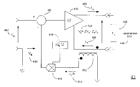
Turning now to FIG. 4, FIG. 4 shows a block diagram of a voltage transmitter
circuit 40 connected to a transmission line 440 having a characteristic
impedance Zo 442.
The block diagram 40 illustrates a use of current feedback-418 from the an
output of a
voltage driver 410 to synthesize a driver circuit whose Thevenin equivalent is
a voltage
generator of amplitude 2Viõ in series with an impedance Z0, similar to the
circuit shown
in FIG. 2A. The input voltage V;r, 402 is summed with a negative feedback
voltage Vfb
420 to provide an input voltage of Vin - Vfb to the voltage driver 410. Since
the voltage
driver 410 has a voltage gain of two, the output voltage Vo 408 of the voltage
driver 410
is Vo = 2Viõ - 2Va,. A transformer 412 having a turns ratio of n senses the
output current
Io 406 and provides the signal Io/n to one input to a multiplier 414. Another
input signal
to the multiplier is the constant value nZo/2 516. Therefore, the output
signal of the
multiplier 414 is Vfb = (Io/n)(nZo/2) = L Z,/2 420. By substituting this value
of Vfb 420
into the expression above for the output voltage Vo 408, the output voltage
Vo=2Vi0-10Zo
This expression for the output voltage Vo 408 has the form of the output
voltage of FIG.
2A and FIG. 2B, and illustrates how the driving source impedance may be
matched to
the characteristic impedance of a transmission without the use of power
consuming
components. Summarizing, the output current 406 is measured, scaled and
multiplied by
an impedance nZJ2, resulting in the feedback voltage Vt, 420. The feedback
voltage Vtb
420 is subtracted from the input voltage Viõ 402 and fed to an input of the
voltage driver
CA 02401539 2002-08-27
WO 01/65691 PCT/USOI/05580
410, which has a gain of two. The scaling and multiplication may be
accomplished on a
current-to-voltage converter, the output driver, or through use of digital
filtering
techniques in a Digital Signal Processor (DSP). Note that the voltage driver
410 will
only generate the voltage seen by the line V0, even if the Thevenin equivalent
circuit has
5 a voltage generator of twice this value. This method achieves the objective
of impedance
matching without wasting power or dropping a voltage in an impedance-matching
resistor. This method is also adaptable to the use of a DSP'to enable more
accurate and
adaptive matching through digital signal processing techniques. It also allows
full duplex
communication over the same transmission line.
10 Turning now to FIG. 5, FIG. 5 shows a block diagram of a current
transmitter
circuit 50 connected to a transmission line 540 having a characteristic
impedance Zo 542.
The block diagram 50 illustrates a use of output voltage feedback Vo 508 from
an output
of a transconductance driver 510 to synthesize a driver circuit 50 whose
Norton
equivalent circuit is a current generator of amplitude L = kV;,, 506 having an
internal
15 shunt impedance Zg = Z0, the characteristic impedance of the line, and a
transconductance of k, similar to FIG. 3A. The input voltage Vin 502 is summed
with a
negative feedback voltage Va, 520 to provide an input voltage of Vin - Vtb to
the
transconductance driver 510. Since the transconductance driver 510 has a
transconductance of 2k, the output current I3 506 of the transconductance
driver 510 is Io
= 2kV;0 - 2kVa,. An amplifier 512 senses the output voltage Vo 508 and
provides this
signal V,, 508 to one input of a multiplier 514. Another input signal to the
multiplier is
the constant value 1/2kZo 516. Therefore, the output signal of the multiplier
514 is Vfb _
Vo/2kZ0 520. By substituting this value of Va, 520 into the expression above
for the
output current L 506, the output current
CA 02401539 2002-08-27
WO 01 /65691 PCT/USOI/05580
16
Io = 2kV;. - V./Z.
This expression for the output current I,, 506 has the form of the output
current of FIG.
3A and FIG. 3B, and illustrates how the driving source impedance may be
matched to
the characteristic impedance of a transmission without the use of power
consuming
components. Summarizing, the output voltage 508 is measured and multiplied by
an
admittance 1/2kZo, resulting in the feedback voltage Va, 520. The feedback
voltage Va,
520 is subtracted from the input voltage V;,, 502 and fed Wan input of the
transconductance driver 510, which has a gain of 2k, where k is the
transconductance of
the transconductance driver 510. The scaling and multiplication may be
accomplished on
an amplifier, the output driver, or through use of digital filtering
techniques in a Digital
Signal Processor (DSP). This method achieves the objective of impedance
matching
without wasting power or dropping a voltage in an impedance-matching resistor.
This
method is also adaptable to the use of a DSP to enable more accurate and
adaptive
matching through digital signal processing techniques. It also allows full
duplex
communication over the same transmission line.
Turning now to FIG. 6A, FIG. 6A shows a circuit diagram 60 of a voltage
transmitter circuit using an inductive sensor connected to a transmission line
640 having
a characteristic impedance Z,, 642. The voltage transmitter circuit of Fig. 6A
comprises a
first operational amplifier 614 and a second operational amplifier 616 having
input and
outputs connected to a resistor network 618. An input voltage V;" 602 is
connected to
one terminal of an input impedance nZo/4 603. Another terminal of the input
impedance
nZc/4 603 connects a summing junction 620. An output voltage Vo 608 is derived
between an output terminal of the first amplifier 614 and an output terminal
of the
second amplifier 616. The voltages at the output terminals of the amplifiers
are mirror
CA 02401539 2002-08-27
WO 01/65691 PCT/USO1/05580
17
images of each other. That is, when the output terminal of the first amplifier
is at given
voltage, the output terminal of the second amplifier is at an equal voltage of
opposite
polarity. The magnitude of the voltage at the output terminal of each
amplifier 614, 616
is V0/2. A terminal of a feedback impedance nZo/2 604 is connected to the
output
terminal of the second amplifier 616 and another terminal of the feedback
impedance
nZd2 604 is connected to the summing junction 620. A transformer 612 senses
the
output current Io 606 and provides a scaled feedback current If, = 1,/n 622 to
the
summing junction 620. By summing the currents into the summing junction, an
expression for the output voltage may be derived
V. = 4Vi^ - I.Z.
This expression for the output voltage Vo 608 has the form of the output
voltage of FIG
2A and FIG. 2B, and illustrates how the driving source impedance may be
matched to
the characteristic impedance of a transmission without the use of power
consuming
components.
Turning now to FIG. 6B, FIG. 6B shows a circuit diagram 65 of a voltage
transmitter circuit using a resistive sensor connected to a transmission line
690 having a
characteristic impedance Zo 692. FIG. 6B is similar to FIG. 6A, except that a
current
sensing resistor R, 662, a differential amplifier 660 with a gain of A and a
resistor nRs/A
674 have replaced the current sensing transformer of FIG. 6A.The inputs of the
amplifier
660 are connected to the terminals of the sensing resistor RS 662. The output
current Io
656 through the sensing resistor RS 662 creates a voltage that is detected by
the amplifier
660. The output of the amplifier 660 is connected to a terminal of the
resistor nRs/A 674
and another terminal of the resistor nRs/A 674 is connected to a summing
junction 670.
The voltage transmitter circuit of Fig. 6B further comprises a first
operational amplifier
CA 02401539 2002-08-27
WO 01/65691 PCT/USOI/05580
18
664 and a second operational amplifier 666 having input and outputs connected
to a
resistor network 668. An input voltage Vin 652 is connected to one terminal of
an input
impedance nZo/4 653. Another terminal of the input impedance nZo/4 653
connects the
summing junction 670. An output voltage Vo 658 is derived between an output
terminal
of the first amplifier 664 and an output terminal of the second amplifier 666.
The
voltages at the output terminals of the amplifiers are mirror images of each
other. That
is, when the output terminal of the first amplifier is at given voltage, the
output terminal
of the second amplifier is at an equal voltage of opposite polarity. The
magnitude of the
voltage at the output terminal of each amplifier 664, 666 is Vo/2. A terminal
of a
feedback impedance nZo/2 654 is connected to the output terminal of the second
amplifier 666 and another terminal of the feedback impedance nZ0/2 654 is
connected to
the summing junction 670. By summing the currents into the summing junction,
an
expression for the output voltage may be derived:
V. = 4Vin - IoZ0
This expression for the output voltage Vo 658 has the form of the output
voltage of FIG
2A and FIG. 2B, and illustrates how the driving source impedance may be
matched to
the characteristic impedance of a transmission without the use of power
consuming
components.
Turning now to FIG. 7, FIG. 7 shows a circuit diagram 70 of a DSP
implementation of a voltage transmitter connected to a transmission line 740
having a
characteristic impedance Zo 742. The amplifiers 714, 716, resistor network
718, input
resistor 703, feedback resistor 704, and transformer 712 are similar to those
corresponding elements shown in FIG. 6A. The voltage transmitter circuit of
Fig. 7
comprises a first operational amplifier 714 and a second operational amplifier
716
CA 02401539 2002-08-27
WO 01/65691 PCT/US01/05580
19
having input and outputs connected to a resistor network 718. An input
resistor 703
connects between an output of an interpolation filter 728 and a summing
junction 734. A
feedback resistor 704 connects between the summing junction 734 and an output
of the
second amplifier. An output voltage Vo 708 is derived between an output
terminal of the
first amplifier 714 and the output terminal of the second amplifier 716. The
voltages at
the output terminals of the amplifiers are mirror images of each other. That
is, when the
output terminal of the first amplifier is at given voltage, the output
terminal of the
second amplifier is at an equal voltage of opposite polarity. The magnitude of
the
voltage at the output terminal of each amplifier 714, 716 is VO/2. A
transformer 712
senses the output current k 706 and provides a scaled feedback current L/n to
the
summing junction 736 of an I/V converter 730. A feedback resistor 732 connects
between an output of the I/V converter 730 and the summing junction 736 of the
I/V
converter 730. The output of the I/V converter 730 is connected to the input
of an anti-
aliasing filter 720. An output of the anti-aliasing filter 720 is connected to
an input of an
analog-to-digital (A/D) converter 722. Outputs from the A/D converter 722 are
connected to a DSP 724. Outputs from the DSP 724 are connected to the inputs
of a
digital-to-analog (D/A) converter 726. An output from the D/A converter 726 is
connected to the interpolation filter 728. Normally the DSP generates the
signals to be
transmitted over the transmission line, functioning as a modem. Alternatively,
a digital
input voltage V;,, 702 is connected an input terminal of the DSP. By
performing scaling
and feedback functions in a DSP 724, intelligence is added to the process that
allows
sophisticated and adaptive matching of the characteristic impedance Zo of the
transmission line. The DSP 724 may send a voltage signal Vo to the line,
measure the
resulting current and calculate a transfer function, such as nV/I. With
sufficient over-
CA 02401539 2002-08-27
WO 01/65691 PCT/US01/05580
sampling to avoid excessive phase shift, the line impedance may be matched by
multiplying the line current to by a suitable transfer function and
subtracting the result
from twice the intended output signal V0. For full duplex operation, the
received signal
may be obtained by digitally subtracting the transmitted signal from the line
voltage Vo
5 measured by a receiver. Since the invention requires the use of line
impedance models,
with a DSP, these models are no longer limited to simple passive network
elements.
Turning now to FIG. 8A, FIG. 8A shows a representative flow diagram 80 of a
program executed in the DSP of FIG. 7. The DSP is started 802 whenever it is
initially
powered on or reset. A first step is an execution of an initialization routine
804. The
10 details of the initialization routine 804 are described in the description
of FIG. 8B. The
DSP then reads a value representing an input voltage 806, associates a current
time value
with the input voltage 808, and adjusts the time value for a time domain
filter delay 810.
Concurrently with these steps, the DSP reads a value' representing an output
current Io/n
from an A/D converter 812, calculates an error from a predicted current and
updates time
15 domain filter 813, and applies the output current value to a nZo/2 time
domain filter 814.
The DSP then subtracts the filtered output current value from the input
voltage value
816, and provides the resultant value to a D/A converter. If the DSP operation
is to be
terminated 820, the process is ended 822. If not terminated 820, the process
beginning
with concurrently reading input voltage values 806 and reading output current
values
20 812 is repeated. As an alternative to the initialization routine 804
described in FIG. 8B,
the initialization routine may be limited to setting initial parameters of the
time domain
filter for synthesizing an output impedance of approximate value. Then,
referring to FIG.
8A, the DSP would read the output current 812, calculate an error from a
predicted
current and update the time domain filter 813 with a fraction of the error to
improve the
CA 02401539 2002-08-27
WO 01/65691 PCT/USOI/05580
21
matching in a recursive manner. These updated values would then be used to
adjust the
output voltage 816.
Turning now to FIG. 8B, FIG. 8B shows a flow diagram 85 of an initialization
routine depicted as step 804 in FIG. 8A. If the DSP requires initialization,
as described
in the description of FIG. 8A, the initialization routine is started 850. A
value of the
characteristic impedance Zo of the transmission line is set to approximately
match the
transmission line and this value is applied to a time domain filter 852. For
example, an
approximate value of 600 ohms is used for telephone lines, 120 ohms for
twisted pair, or
50 ohm for coaxial cable. The DSP then initiates a request to a receiver at
the opposite
end of the transmission line to present a short-circuit for a fixed amount of
time 854,
simulates a short-circuit output by setting an output voltage to a constant
856, and
measures the value of an output current to find values for a short-circuit
impedance Z;s
versus frequency 858. The DSP then initiates a request to the receiver at the
opposite end
of the transmission line to present an open-circuit for a fixed amount of time
860,
simulates an open-circuit output by setting an output voltage to zero and
setting Zo to a
high value 862, and measures the value of the output current to find values
for an open
circuit impedance Z10 versus frequency 864. The DSP then computes values for
the
characteristic impedance Zo = (Z;, Z0)"2 versus frequency 866 and sets time
domain
filter parameters to match Zo versus frequency 869. Control is then returned
to the main
program 870.
Although the present invention has been described in detail with reference to
certain preferred embodiments, it should be apparent that modifications and
adaptations
to those embodiments may occur to persons skilled in the art without departing
from the
spirit and scope of the present invention as set forth in the following
claims.