Note : Les descriptions sont présentées dans la langue officielle dans laquelle elles ont été soumises.
CA 02403496 2002-09-16
w 1 -
TITLE OF THE INVENTION
SEQUENTIAL MESA AVALANCHE PHOTODIODE CAPABLE OF
REALIZING HIGH SENSITIZATION AND METHOD OF
MANUFACTURING THE SAME
BACKGROUND OF THE INVENTION
The present invention relates to a sequential mesa
avalanche photodiode and a method of manufacturing
the same, and in particular, to a sequential mesa
avalanche photodiode having a sequential mesa structure
in which, in an avalanche photodi.ode to be used as a
light receiving element for converting a light signal
to an electric signal in an optical communication
network or the like, high sensitization can be realized
and the fabrication costs of modularization can be
greatly decreased, and to a method of manufacturing
the same.
As is well-known, recently, the signal speed of
light signals used in optical communication networks
has been made much more high-speed.
In accordance therewith, making the speed more
high-speed has been required of light receiving
elements built in optical communication equipment
transmitting and receiving such light signals.
Further, in such light receiving elements, it is
required that even low level light signals can be
precisely received.
As such a light receiving element receiving
CA 02403496 2002-09-16
- 2 -
high-speed and weak light signals, generally,
an avalanche photodiode (hereinafter, abbreviated APD)
has been put into practice.
In such an APD, in a state in which a depletion
region is formed by applying reverse-bias voltage to
a pn junction formed by a pair of semiconductor layers
whose conductive types are different from one another,
when an electromagnetic wave of a light signal or
the like is incident from the exterior, a pair of
an electron and a positive hole i.s generated.
Further, this pair of the electron and the
positive hole is multiplied by the avalanche phenomenon
in the APD, and taken out as voltage or electric
current to the exterior.
There are various ways of classifying APDs.
When classifying structurally, there are a planar type
and a mesa type, and when classifying by main carrier,
there are a positive hole type and an electron type.
Here, a sequential mesa structure used regardless
of the type of the main carrier will be described.
Generally, in order to aim for making the APD
high-speed, the mesa type, not the planar type, is
generally used as the shape of the APD.
This is for decreasing the electric capacity of
the APD element itself in order to make the APD high-
speed.
In order to increase the permissible
CA 02403496 2002-09-16
- 3 -
light-receiving current as an APD element, there is the
need to remove the bias of the light-receiving current
density flowing through the interior of the mesa
portion.
Therefore, in a mesa type APD element, the shape
of the mesa must be made to be isotropic, namely, as
shown in FIG. 9B, formed sonically as viewed from the
top surface of a substrate.
Moreover, in a mesa type APD element, when the
shape of the mesa is formed to be conical, attention
must be paid such t=hat the crystallinity of the cross-
section of the mesa is not damaged.
Therefore, in a mesa type APD element, when the
shape of the mesa is fabricated, diffusive wet-etching
by an etchant which is not anisotropic is necessary.
By applying this diffusive wet-etching, the
sequential mesa shape, which is a shape (generally,
conical) in which the mesa diameter (cross-sectional
area) widens as it approaches the substrate, can be
obtained.
Accordingly, the sequential mesa type APD is
generally used for making the APD high-speed.
Further, as APDs using positive holes as the main
carrier, there are an APD in which the above-described
pn junction is formed by epitaxial growth, and an APD
in which the pn junction is formed by Zn diffusion.
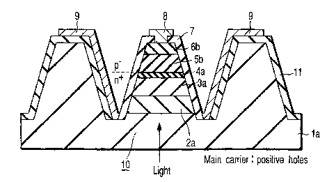
FIGS. 9A and 9B rest>ectively show
CA 02403496 2002-09-16
- 4 -
a cross-sectional view and an external perspective view
of a sequential mesa type APD, in accordance with a
prior art, which has a sequential mesa structure and in
which positive holes are used as the main carrier and
the pn junction is formed by epitaxial growth.
Hereinafter, on the basis of FIGS. 9A and 9B, the
structure of the sequential mesa type APD according to
the prior art will be described.
Namely, in the sequential mesa type APD according
to the prior art, as shown in FIGS. 9A and 9B,
an n-type buffer layer 2a, an n-type light absorbing
layer 3a, an n-type electric field relaxation layer 4a,
an n-type multiplying layer 5a, and a p-type contact
layer 6b are successively formed by epitaxial growth by
using an MOVPE (organometallic vapor phase epitaxial
growth) method on an n-type semiconductor substrate la.
Therefore, a conical sequential mesa portion 10 is
formed by wet-etching from above.
Next, after a protective layer 7 is coated on the
sequential mesa portion 10, a p electrode 8 contacting
the p-type contact layer 6b is formed.
Further, at the both sides of the sequential mesa
portion 10, an n electrode 9 is attached, via
a protective layer 11, to another mesa portion formed
for attaching electrodes.
As shown by the arrcw in FIG. 9A, light incident
on the APD from the bottom surface of the semiconductor
CA 02403496 2002-09-16
-- 5 -
substrate la penetrates through i:he semiconductor
substrate la and the buffer layer 2a and is absorbed at
the light absorbing layer 3a, so that a pair of
an electron and a positive hole is generated.
Among the pair of the electron and the positive
hole generated in this way, the electron moves to the n
electrode 9 via the semiconductor substrate la, and the
positive hole is multiplied at the multiplying layer
5a, and moves to t:he p electrode 8 via the contact
layer 6b.
In order to make the positive hole be the main
carrier among the pair of the electron and the positive
hole, a great number of the carriers of the light
absorbing layer 3a must be electrons.
Namely, the conductive type of the light absorbing
layer 3a must be n type.
Such a sequential mesa type APD uses a so-called
SAM (Separate Absorption and Multiplication) structure,
in which the multiplying layer 5a and the light
absorbing layer 3a are separated by the electric field
relaxation layer 4a such that a low electric field
intensity is applied to the lighi= absorbing layer 3a
while a high electric field intensity is applied to the
multiplying layer 5a.
In this case, becau~~e the electric field intensity
of the n-type light absorbing layer 3a is suppressed by
the electric field relaxation layer 4a, the conductive
CA 02403496 2002-09-16
-- 6 -
type of the electric field relaxation layer 4a is the
same n type as that of th.e light absorbing layer 3a.
Because such a sequential mesa type APD has
a function avalanche-multiplying the light exciting
carrier, the crystallinity of the above-described
layers is considered to be extremely important.
Note that, in such a sequential mesa type APD, the
epitaxial growth itself of each layer can be carried
out, in theory, on a semiconductor substrate which is
any of an n-type semiconductor substrate, a p-type
semiconductor substrate, or a semi-isolated
semiconductor substrate.
As described above, in the sequential mesa type
APD, when considering the fact that light-receiving
current flows via the semiconductor substrate, the
semiconductor substrate which is used must be an n-type
or a p-type semiconductor substrate.
However, as shown in FIGS. 9A and 9B, because
a dopant such as Sn, S or the like included in the
semiconductor substrate 7_a does not diffuse during
the epitaxial growth, the n-type semiconductor
substrate 1a is suitable as a substrate for the
epitaxial growth of each semiconductor layer.
On the other hand, in the p-type semiconductor
substrate, there are problems such as the Zn included
in the semiconductor substrate diffuses during the
epitaxial growth, there =.s the need to form a thicker
CA 02403496 2002-09-16
- 7 -
buffer layer by epitaxial growth in order to prevent
the Zn from diffusing, and because the n-type
semiconductor substrate layer is formed by epitaxial
growth after the p-type semiconductor substrate is
formed by epitaxial growth, the time after the
epitaxial growth of the p-type semiconductor layer
becomes longer. Thus, diffusion of the 2n which is the
dopant in the p-type semiconductor layer formed by the
epitaxial growth easily arises.
Namely, the p-type semiconductor substrate
having such problems is not generally suitable for
a sequential mesa type APD in which crystallinity is
considered to be extremely important.
Accordingly, it is preferable that the n-type
semiconductor substrate la is used as the sequential
mesa type APD in order to epitaxially grow
a semiconductor layer having good quality
crystallinity.
In this way, in order to obtain a good light-
receiving characteristic in a sequential mesa type APD
in which the positive holes are the main carrier and
the pn junction is formed by epit.axial growth,
the n-type light absorbing layer 3a and the n type
field relaxation layer 4a are necessary, and the
semiconductor subst=rate which is used is preferably
the n-type semiconductor substrate la.
Further, as described above, in a sequential mesa
CA 02403496 2002-09-16
_ g _
type APD in which t:he positive holes are the main
carrier and the pn junction is formed by the epitaxial
growth, as shown in FIGS. 9A and 9B, the p-type contact
layer 6b is used in order to ensure an ohmic electrode
in the p electrode 8.
At the time of epi.taxial growth of the contact
layer 6b, the contact layer 6b is doped to p type by
using a p-type dopant such as Zn or the like.
Note that, in order to obtain the ohmic electrode,
the p-type carrier density of the contact layer 6b is
preferably set to be as high as possible, for example,
about 5 x 10¹⁸ (cm-3) or more.
Note that the above-described MOVPE method or the
like is mainly used as a growth method (manufacturing
method) of the contact layer 6b.
Further, due to the Zn which is the dopant of the
contact layer 6b being diffused in the n-type electric
field relaxation layer 4a, the conductive type of
the multiplying layer 5a is made to be n type so that
the appropriate internal electric field intensity
distribution in the direction perpendicular to the
n-type semiconductor substrate 1a is not destroyed.
Accordingly, the pn junction in the sequential
mesa type APD is formed by the p-type contact layer 6b
and the n-type multiplying layer 5a.
Note that, in this case, the carrier density of
the p-type contact layer 6b is particularly high as
CA 02403496 2002-09-16
-- 9 -
compared with the carrier density of the n-type
multiplying layer 5a.
Therefore, it is ideal that the sequential mesa
type APD, in which the positive holes are used as the
main carrier and the pn junction is formed by epitaxial
growth, has the structure shown in FIGS. 9A and 9B.
Namely, because the sequential mesa type APD
basically does not use a Zn diffusing process to be
described later, there is the advantage that the
manufacturing process (the process steps) can be
simplified.
Further, because the sequential mesa type APD uses
an n-type semiconductor in the electric field
relaxation layer 4a which is difficult to be
manufactured by a p-type semiconductor, there is the
advantage that MOVPE, which can epitaxially grow at the
wafer a semiconductor layer having high crystallinity,
can be used as the method of manufacturing
the sequential mesa type APD.
Next, a sequential mesa type APD, which has
a sequential mesa structure and in which positive holes
are used as the main carrier and the pn junction is
formed by 2n diffusion, will be described.
The structure itself of such a sequential mesa
type APD is the same as the structure of the sequential
mesa type APD shown in FIGS. 9A and 9B.
As described above, in order to acquire excellent
CA 02403496 2002-09-16
- 10 -
characteristics at the sequentia7_ mesa type APD in
which the positive holes are the main carrier,
the n-type light absorbing layer 3a and the n-type
electric field relaxation. layer 4a are necessary, and
it is preferable to use the n-type semiconductor
substrate la. This is also true in the case of
a sequential mesa type APD in which the pn junction is
formed by Zn diffusion, and in the case of the above-
described sequential mesa type APD, in which the pn
junction is formed by epi_taxial growth.
Further, the contact. layer 6b is made to be p type
by diffusing Zn therein by a Zn diffusion method
in order to ensure an ohmic electrode in the
p electrode 8.
Note that, in order to obtain the ohmic electrode,
the p-type carrier densit=y of the contact layer 6b is
preferably set to be as high as possible, for example,
about 5 x 10¹⁸ (cm-3) or more.
Further, in the Zn diffusing method, by heating
the Zn raw material and the wafer contained in
a container filled with an inert gas atmosphere, the Zn
is diffused from the surface of the wafer to the
interior of the wafer.
At this time, in order to carry out sufficient Zn
diffusion, there is the need to control the gas
pressure of the inert gas atmosphere so as to maintain
a relatively high value by using an exclusively-used
CA 02403496 2002-09-16
- 11 -
controller, and there is the problem that the
manufacturing process (process st=eps) is complicated.
The Zn diffused in this way remains in the contact
layer 6b, and the p-type carrier density is enhanced to
a degree at which an ohmic electrode can be obtained,
for example, to 5 ;~ 1018 ( cm-3 ) or more .
Note that, at this t=ime, because the Zn is not
diffused in the multiplying layer 5a, the conductive
type of the multiplying 7_ayer 5a is n type as is.
In accordance therewith, the pn junction is formed
by the p-type contact layer 6b, in which the p-type
carrier density is increased by Zn diffusion, and the
n-type multiplying layer 5a.
As a result, also in the case of a sequential mesa
type APD in which positive holes are used the main
carrier and the pn junction is formed by Zn diffusion,
the structure shown in FIGS. 9A and 9B is ideal.
Further, the sequential mesa type APD in which
the pn junction is formed by Zn diffusion has the
advantage that. the desired pn junction can be formed by
appropriately setting the diffusing conditions of
the Zn.
Further, the sequential mesa type APD in which
the pn junction is formed by Zn diffusion also has
the advantage that, because an n-type semiconductor is
used as the electric field relaxation layer 4a which is
difficult to fabricate by a p-type semiconductor,
CA 02403496 2002-09-16
- 12 -
the MOVPE method, by which a highly crystalline
semiconductor layer can be ep:itaxially grown on the
wafer, can be used as the manufacturing method.
On the other hand, because the sequential mesa
type APD uses a Zn diffu~~ing process, the sequential
mesa type APD has the drawback that the manufacturing
process (process steps) is complicated due to the
above-described reasons.
Next, the sequential mesa type APD, which has
a sequential mesa structure and in which electrons are
used as the main carrier and the pn junction is formed
by epitaxial growth, will be described.
FIG. 10 shows a cross-sectional view of the
sequential mesa type APD which has a sequential mesa
structure and in which electrons are used as the main
carrier and the pn junction is formed by epitaxial
growth.
Note that, in this FIG. 10, portions which are
the same as those of the sequential mesa type APD shown
in FIG. 9A are denoted by the same reference numerals.
Further, an external perspective view of the
sequential mesa type APD, which is shown in FIG. 10 and
in which electrons are used as the main carrier and the
pn junction is formed by epitaxial growth, is the same
as in FIG. 9B, and thus, illustration is omitted.
Namely, as shown in FIG. 10, in the sequential
mesa type APD in which electrons are used as the main
CA 02403496 2002-09-16
- 13 -
carrier and the pn junction is formed by epitaxial
growth, after the n-type buffer layer 2a, the n-type
multiplying layer 5a, the p-type electric field
relaxation layer 4b, the p type light absorbing
layer 3b, a p-type window layer 13b, and the p-type
contact layer 6b are successively formed by epitaxial
growth on the n-type semiconductor substrate la by
using an epitaxial growth method, the conical
sequential mesa portion 10 is formed by wet-etching
from above.
Further, after the protective layer 7 is coated on
the sequential mesa portion 10, the p electrode 8
contacting the p-type contact layer 6b is formed.
Further, on the both sides of the sequential mesa
portion 10, the n electrodes 9 are attached, via the
protective layer 11, to another mesa portion formed for
attaching electrodes.
In such a sequential mesa type APD in which
electrons are the main carrier, as shown by the arrow
in FIG. 10, light incident from the bottom surface of
the semiconductor substrate la penetrates through the
semiconductor substrate :La, the buffer layer 2a, the
multiplying layer 5a, and the electric field relaxation
layer 4b and is absorbed at the light absorbing
layer 3b, so that a pair of an electron and a positive
hole is generated.
Among the pair of the electron and the positive
CA 02403496 2002-09-16
- 14 -
hole generated in this way, the electron is multiplied
at the multiplying layer 5a and moves to the n
electrode 9 via the n-type semiconductor substrate la,
and the positive hole moves to the p electrode 8 via
the contact layer 6b.
In order to make the positive hole be the main
carrier among the pair of the electron and the positive
hole, a great number of carriers of the light absorbing
layer 3b must be positive holes.
Namely, in this case, the conductive type of the
light absorbing layer 3b must be p type.
In such a sequential mesa type APD in which
electrons are the main carrier, the above-described SAM
structure, in which the multiplying layer 5a and the
light absorbing layer 3b are separated by the electric
field relaxation layer 4b such that a low electric
field intensity is applied to the light absorbing layer
3b while a high electric field intensity is applied to
the multiplying layer _'ia, is used.
In this case, because the electric field intensity
of the p type light absorbing layer 3b is suppressed by
the electric field relaxation layer 4b, the conductive
type of the electric field relaxation layer 4b is p
type which is the same as that of the light absorbing
layer 3b.
Further, because such a sequential mesa type APD
in which electrons ar_e the main carrier has a function
CA 02403496 2002-09-16
- 15 -
avalanche-multiplying the light exciting carrier, the
crystallinity of the above-described layers is
considered to be extremely important.
In order to obtain excellent crystallinity of each
semiconductor layer, for the same reasons as in the
case of the sequential mesa type APD described in
FIGS. 9A and 9B in which positive holes are the main
carrier, the semiconductor substrate which is used is
preferably the n-type semiconductor substrate la.
Moreover, in order. t=o improve the accuracy of the
electric field intensity distribution in the sequential
mesa portion 10 in the direction perpendicular to the
semiconductor substrate la, because the pn junction is
preferably formed between the p-type electric field
relaxation layer 4b and the multiplying layer 5a, the
multiplying layer 5a is n type.
Such a formed position of the pn junction is also
preferable for making estimation of the amount of
decrease in the electric field intensity in the
multiplying layer 5a be unnecessary.
Accordingly, in the sequential mesa type APD in
which electrons are the main carrier, the pn junction
is formed by the p-type electric field relaxation
layer 4b and the multiplying layer 5a.
In this way, in order to obtain excellent light-
receiving characteristics in a sequential mesa type APD
in which the electrons are the main carrier and the pn
CA 02403496 2002-09-16
- 16 -
junction is formed by epitaxial growth, the p type
light absorbing layer 3b, the p-type electric field
relaxation layer 4b, and the n-type multiplying layer
5a are necessary, and the semiconductor substrate which
is used is preferably the n-type semiconductor
substrate la.
In such a sequential- mesa-type APD, the window
layer 13b also is necessary in order to prevent the
electrons which are a light exciting carrier from
diffusing/moving to the contact :Layer 6b.
Note that GS-MBE (gas-molecule beam epitaxy), MBE
(molecule beam epitaxy), and the like are mainly used
as the epitaxial growth method.
Further, in order to ensure the ohmic electrode of
the p electrode 8, the conductive type of the contact
layer 6b is p type.
Moreover, at the time of epitaxial growth, the
contact layer 6b is doped to a p type by using a p-type
dopant such as Be or the like.
Note that, in order to obtain the ohmic electrode,
the p-type carrier density of the contact layer 6b is
preferably set to be as high as possible, for example,
about 5 x 101 (cm-3) or more.
Accordingly, in a sequential mesa type APD in
which electrons are the main carrier, the structure
shown in FIGS. 9A and 9B is ideal, and because
electrons having a light effective mass are the main
CA 02403496 2002-09-16
- 17 -
carrier, there is the feature that it is advantageous
with respect to the point of high-speed performance.
However, in the APDs having the sequential mesa
structures shown in FIGS. 9A, 9B and FIG. 10, there are
still the following problems which must be improved.
Firstly, in the sequential mesa type APD in which
positive holes are the main carrier, or also in the
sequential mesa type APD in which electrons are the
main carrier, there is the problem that, in each
semiconductor layer forming the sequential mesa
portion 10, except for the case of selectively
diffusing Zn at a specific portion in the surface
parallel to the semiconductor substrate, it is
difficult for the in-surface distribution of electric
field intensity in a surface parallel to the
semiconductor substrate to concentrate at the central
portion of the mesa by only the epitaxial growth
process.
FIG. 3 shows measured results of the light-
receiving sensitivity distribution characteristic of
a sequential mesa type AL~D whose light-receiving
diameter is 40 Vim.
Concretely, FIG. 3 shows measured values of
light-receiving current (~A) obtained between the p
electrode 6 and the n electrode 9 at each position (gym)
in a case in which the irradiating position of
an extremely thin light beam is successively moved
CA 02403496 2002-09-16
- 18 -
within the aforementioned range of 40 ~,m.
In FIG. 3, characteristic B shows the light-
receiving sensitivity distribution characteristic of
the sequential mesa type APD as shown in FIGS. 9A
and 9B.
As illustrated, characteristic B is a double-
peaked characteristic in which the light-receiving
current at the peripheral portion of the mesa shown by
the positions -20 ~,m, +20 ~,m from the central position
(0) is larger than the light-receiving current at the
central portion of the mesa.
A sequential mesa type APD whose light-receiving
characteristic is a double-peaked characteristic in
this way has the problem that it is difficult to align
the optical axes at the t=ime of actual use when made
into a module, and the yield of the modularization
deteriorates. Because alignment of the optical axes
must be carried out at the central portion of the mesa
at which the light-receiving current is smaller than
that of the peripheral portion of the mesa,
a sufficient light-receiving characteristic cannot be
exhibited. In addition, it is difficult to realize
high sensitization by keeping to a minimum the effects
of the dark current and noise contained in the light-
receiving signal :relating to the problem of
crystallinity described later, and to decrease the
fabricating costs of modularization.
CA 02403496 2002-09-16
- 19
Hereinafter, reasons why these problems arise will
be described.
Because the APD shown in FIGS. 9A and 9B is
a sequential mesa type structure, the more the electric
field intensity increases, the more the carrier of the
positive holes or the electrons is multiplied.
Accordingly, the magnitude of the light-receiving
current shows the magnitude of the electric field
intensity at the pn junction.
It can be said that the electric field intensity
at the periphery of the mesa is higher and the electric
field intensity at the central portion of the mesa is
low in the sequential mesa type APD shown in FIGS. 9A
and 9B.
FIG. 11 shows the way of broadening (width) of
the depletion region (depletion layer) by built-in
potential from the pn junction in the sequential mesa
type APD shown in FIGS. 9A and 9B in which positive
holes are used as the main carrier.
Note that, as described above, because the carrier
density of the p-type contact layer 6b forming the pn
junction is higher than the carrier density of the
multiplying layer 5a, the majority of the depletion
region (depletion layer) is formed at the semiconductor
substrate la side of the pn junction.
As shown in FIG. 11, because this APD has
a sequential mesa structure, the ratio of the
CA 02403496 2002-09-16
- 20 -
cross-sectional area showing the depletion region of
the p-type contact layer 6b structuring the pn junction
and the cross-sectional area showing the depletion
region of the n-type multiplying layer 5a greatly
differs at the central portion of the mesa and at the
peripheral portion of the mesa.
Here, considering from the standpoint of depleting
the pn junction portion, because the APD has
a sequential mesa structure, at the vicinity of the
periphery of the mesa, there is a state in which the
carrier density of the multiplying layer 5a is
substantially higher than at the central portion of the
mesa.
In contrast, at the contact layer 6b, conversely,
there is a state in which the carrier density is weak.
However, because the carrier density is originally high
at the contact layer 6b, even if it is in a state in
which the carrier density is substantially weak,
the effect is small.
As a result, in the sequential mesa type APD,
the way of broadening (width) of the depletion region
is shorter (narrower) than the way of broadening
(width) of the central portion.
Namely, it can be understood that the electric
field intensity at the peripheral portion of the mesa
is higher than that at the central portion of the mesa
in the sequential mesa type APD.
CA 02403496 2002-09-16
- 21 -
FIG. 12 shows the way of broadening (width) of
the depletion region (depletion layer) by built-in
potential from the pn junction portion in the
sequential mesa type APD as shown. in FIG. 10 in which
electrons are used as the main carrier.
In this sequential mesa type APD, the carrier
density of the p-type electric field relaxation layer
4b forming the pn junction is higher than the carrier
density of the multiplying layer 5a. Thus, as shown in
FIG. 12, in accordance with the principles of charge
neutrality, the way of broadening (width) of the
depletion region at the vicinity of the periphery of
the mesa is shorter (narrower) than the way of
broadening (width) of the central portion.
Namely, in the sequential mesa type APD, the
electric field intensity at the peripheral portion of
the mesa is higher than that at the central portion of
the mesa.
The reason for this is that, in the sequential
mesa type APD, it is difficult for the in-surface
distribution of field intensity in a surface parallel
to the semiconductor substrate to concentrate at the
central portion of the mesa by only the epitaxial
growth process, so that there is a double-peaked
characteristic in which the light-receiving current at
the peripheral portion of the mesa is greater than the
light-receiving current at the central portion of the
CA 02403496 2002-09-16
- 22 -
mesa.
In this way, in the sequential mesa type APD in
which positive holes or electrons are used as the main
carrier and the pn junction is formed by epitaxial
growth, the way of broadening (width) of the depletion
region at the vicinity of the periphery of the mesa is
shorter (narrower) that at the central portion, and the
electric field intensity at the peripheral portion of
the mesa is higher than at the central portion of the
mesa.
Here, the relationship between the crystallinity
and the light-receiving characteristic of the
sequential mesa type APD will be described.
As described above, a sequential mesa type APD of
this type, the light-receiving current is multiplied by
an avalanche multiplying function.
Further, the noise at the time of the avalanche
multiplying function greatly depends on
the crystallinity of the sequential mesa type APD.
Accordingly, even among light-receiving elements
in which crystallinity is considered to be important,
in particular, the crystallinity of a sequential mesa
type APD is important.
In a sequential mesa type APD, a mesa side surface
10a formed by mesa-etching is provided at the
peripheral portion of the mesa of a sequential mesa
portion 10.
CA 02403496 2002-09-16
- 23 -
Generally, the mesa side surface 10a has a great
number of crystal defects as compared with the interior
portion of the mesa.
Further, the crystal defects adversely affect the
consideration of solutions for decreasing dark current
in the sequential mesa type APD, decreasing noise, high
sensitization, and modular_ization.
Namely, in a sequential mesa type APD in which
positive holes or electrons are used as the main
carrier and the pn junction is formed by epitaxial
growth, as shown by characteristic B of FIG. 3, when
the light-receiving characteristic of the sequential
mesa type APD is dominant at the peripheral portion of
the mesa, the good crystallinity which the central
Z5 portion of the mesa has is not reflected in the light-
receiving characteristic of the entire sequential mesa
type APD. As a result, it is a cause for the light-
receiving characteristic of the entire sequential mesa
type APD to deteriorate, and for it to be difficult to
align optical axes at the time of making the APD
a module, and for the yield of modularization to be
poor, and for the fabricating costs of modularization
to increase.
BRIEF SUMMARY OF THE INVENTION
An object of the present invention is to provide
a sequential mesa type avalanche photodiode which is
achieved on the basis of the above-described
CA 02403496 2002-09-16
- 24 -
circumstances, and in which, in a sequential mesa type
APD in which positive holes or electrons are used as
the main carrier and a pn junction is formed by
epitaxial growth, by making the distribution of the
electric field concentrate at the central portion of
the mesa, the effects of dark current and noise
contained in a light-receiving signal can be kept to
a minimum, and high sensitization can be realized, and
the fabricating costs at the time of modularization of
the APD can be greatly decreased.
Another object of the present invention is to
provide a method of manufacturing a sequential mesa
type avalanche photodiode which is achieved on the
basis of the above-described circumstances, and in
which, in a sequential mesa type APD in which positive
holes or electrons are used as the main carrier and
a pn junction is formed by epitaxial growth, by
making the distribution of the electric field
concentrate at the central portion of the mesa, the
effects of the dark current and noise contained in
a light-receiving signal can be kept to a minimum, and
high sensitization can be realized, and the fabricating
costs at the time of modularization of the APD can be
greatly decreased.
First, the point of interest of the present
invention will be described.
As described above, in a sequential mesa type APD
CA 02403496 2002-09-16
- 25 -
in which the pn junction is formed by only an epitaxial
growth process, it is difficult to concentrate, at
the central portion of the mesa, the in-surface
distribution of the electric field intensity in
a surface parallel to the semiconductor substrate.
Therefore, conventionally, regardless of the fact
that there is the difficulty that the manufacturing
process (process steps) is complicated, the sequential
mesa type APD, in which the pn junction is formed by
using the Zn diffusion process which can make the
distribution of the electric field concentrate at the
central portion of the mesa by selectively diffusing
the Zn at a specific portion in a surface parallel to
the semiconductor substrate, is exclusively used.
The present inventor has used in combination
contrivances for concentrating the distribution of
the electric field at the central portion of the mesa
which has not been carried out in the prior art, in
a sequential mesa type APD in which positive holes or
electrons are used as the main carrier and the pn
junction is formed by only an epitaxial growth process.
From the concept opposite that of a sequential
mesa type APD in which the pn junction is formed by
using the conventional Zn diffusion process, the
present inventor, as a result of diligently searching
for such contrivances, has found that it suffices that
the carrier density of a semiconductor layer which is
CA 02403496 2002-09-16
- 26 -
near to the semiconductor substrate among a pair of
semiconductor layers forming the pn junction is larger
than the carrier density of a semiconductor layer which
is far from the semiconductor substrate among the pair
of semiconductor layers.
In a sequential mesa type APD structured by
satisfying such a relationship, as described above,
the ratio of the cross-sectional areas of the pair of
semiconductor layers structuring the pn junction formed
within the mesa portion is constant at the central
portion of the mesa, and is different at the central
portion of the mesa and at the peripheral portion of
the mesa.
Here, considering from the standpoint of depleting
the pn junction portion, because the APD has a
sequential mesa structure, among the pair of
semiconductor layers structuring the pn junction, at
the vicinity of the periphery of the mesa, there is
a state in which the carrier density of the
semiconductor Layer which is far from the semiconductor
substrate is substantially weaker than at the central
portion of the mesa.
In contrast, at the semiconductor layer which is
near to the semiconductor substrate, conversely, there
is a state in which the carrier density is high.
However, because the carrier density is originally high
at the semiconductor layer which is near to the
CA 02403496 2002-09-16
- 27 -
semiconductor substrate, even if it is in a state in
which the carrier density is substantially high, the
effect is small.
Namely, the way of broadening (width) of the
depletion region at the peripheral portion of the mesa
is greater than the way of broadening (width) of the
depletion region at the central portion of the mesa,
and the electric field intensity at the central portion
of the mesa is greater than the electric field
intensity at the peripheral portion of the mesa.
Thus, in such a sequential mesa type APD according
to the present invention, the component at the central
portion of the mesa contained in the overall light-
receiving characteristic of the APD can be increased,
and the component at the peripheral portion of the mesa
can be decreased.
Accordingly, in such a sequential mesa type APD
according to the present invention, the effects of
the dark current and noise caused due to crystal
defects which are many at the peripheral portion of the
mesa can be kept to a minimum, and decreasing of dark
current, decreasing of noise, and high sensitization in
the overall light-receiving characteristic of the APD
can be attempted. Further, since the yield of
modularizing is improved by making the alignment of the
optical axes at the time of modularizing be easy and
exact, the fabricating costs of modularizing can be
CA 02403496 2002-09-16
- 28 -
greatly decreased.
In such a sequential mesa type APD, the
relationship of the magnitude of the carrier densities
of the pair of semiconductor layers forming the pn
junction is a relationship opposite to the .relationship
of the magnitude of the carrier densities of the pair
of semiconductor layers forming the pn junction in
a conventional sequential mesa type APD in which the pn
junction is formed by a 2n diffusion process.
Next, the background of the difficulty of the idea
of the relationship of the magnitude of the carrier
densities of the pair of semiconductor layers forming
the pn junction will be described.
Namely, in a conventional sequential mesa type APD
in which the pn junction is formed by using a Zn
diffusion process, as described above, the pn junction
is formed by the p-type contact layer 6b, in which the
p-type carrier density is made high by 2n diffusion,
and the n-type multiplying layer 5a.
At this time, it is preferable, for the contact
layer 6b as well, that the p-type carrier density of
the contact layer 6b is set to be as high as possible,
for example, about 5 x 10¹⁸ (cm-2) or more. The gas
pressure of the inert gas atmosphere used for carrying
out sufficient Zn diffusion is controlled so as to
maintain a relatively high value by using an
exclusively-used controller.
CA 02403496 2002-09-16
- 29 -
Namely, in the conventional sequential mesa type
APD in which the pn junction is formed by using a Zn
diffusion process, there is a relationship in which the
carrier density of the p-type contact layer 6b (the
semiconductor layer which is far from the semiconductor
substrate) forming the pn junction is larger than the
carrier density of the n-type multiplying layer 5a
(the semiconductor layer which is near to the
semiconductor substrate).
Accordingly, in the sequential mesa type APD of
the present invention, whose relationship is opposite
to this relationship and in which the pn junction is
formed by epitaxial growth, it would not be generally
thought to make the carrier density of the
semiconductor layer which is near to the semiconductor
substrate among the pair of semiconductor layers
forming the pn junction, larger than the carrier
density of the semiconductor layer which is far from
the semiconductor substrate among the aforementioned
pair of semiconductor layers.
Further, in the sequential mesa type APD of the
present invention in which the pn junction is formed by
epitaxial growth, the semiconductor layer which is far
from the semiconductor substrate among the pair of
semiconductor layers forming the pn junction, is formed
separate from and at the lower layer of the p-type
contact layer, and the gas pressure of the inert gas
CA 02403496 2002-09-16
- 30 -
atmosphere used for 2n diffusion for obtaining an ohmic
electrode of the contact layer 6b may be maintained at
a relatively low value.
Accordingly, in accordance therewith, in the
sequential mesa type APD of the present invention in
which the pn junction is formed by epitaxial growth, it
would not be generally thought to make the carrier
density of the semiconductor layer which is near to the
semiconductor substrate among the pair of semiconductor
layers forming the pn junction, larger than the carrier
density of the semiconductor layer which is far from
the semiconductor substrate among the aforementioned
pair of semiconductor layers.
In order to achieve the above object, there is
provided a sequential mesa type avalanche photodiode
comprising:
a semiconductor substrate; and
a sequential mesa portion formed on
the semiconductor substrate, a plurality of
semiconductor layers which include a light absorbing
layer and a multiplying layer being laminated by
epitaxial growth, in the sequential mesa portion, and
a pair of semiconductor layers which form a pn junction
being included in the plurality of semiconductor
layers, wherein
the carrier density of a semiconductor layer which
is near to the semiconductor substrate among the pair
CA 02403496 2002-09-16
- 31 -
of semiconductor layers is larger than the carrier
density of a semiconductor layer which is far from the
semiconductor substrate among the pair of semiconductor
layers, and
in accordance therewith, in the sequential mesa
type avalanche photodiode, light-receiving current
based on movement of electrons and positive holes
generated in the sequential mesa portion when light is
incident from the semiconductor substrate toward the
light absorbing layer is larger at a central portion
than at a peripheral portion of the sequential mesa
portion.
According to a second aspect of the present
invention, there is provided a sequential mesa type
avalanche photodiode according to the first aspect,
wherein the semiconductor substrate is structured from
an n-type semiconductor substrate, and any of the
electrons or the positive holes are the main carrier.
According to a third aspect of the present
invention, there is provided a sequential mesa type
avalanche photodiode according to the second aspect,
wherein the n-type semiconductor substrate is a
semiconductor substrate formed from n+-type InP.
According to a fourth aspect of the present
invention, there is provided a sequential mesa type
avalanche photodiode according to the second aspect,
wherein the semiconductor layer which is near to the
CA 02403496 2002-09-16
- 32 -
n-type semiconductor substrate among the pair of
semiconductor layers is an n-type semiconductor layer,
and the semiconductor layer which is far from the
n-type semiconductor substrate among the pair of
semiconductor layers is a p-type semiconductor layer.
According to a fifth aspect of the present
invention, there is provided a sequential mesa type
avalanche photodiode according to the fourth aspect,
wherein the n-type semiconductor layer (4a, 14a, 15a)
is an n-type electric field relaxation layer (4a),
and the p-type semiconductor layer (5b, 14b, 12b) is
a p-type multiplying layer (5b), and the positive holes
are the main carrier.
According to a sixth aspect of the present
invention, there is provided a sequential mesa type
avalanche photodiode according to the fifth aspect,
wherein the n-type electric field relaxation layer is
an electric field relaxation layer formed from n+-type
InP, and the p-type multiplying layer is a multiplying
layer formed from p--type InP.
According to a seventh aspect of the present
invention, there is provided a sequential mesa type
avalanche photodiode according to the fourth aspect,
wherein the n-type semiconductor layer is an n-type
electric field relaxation layer, and the p-type
semiconductor layer is a p-type electric field
concentration layer, and the positive holes are the
CA 02403496 2002-09-16
- 33 -
main carrier.
According to an eighth aspect of the present
invention, there is provided a sequential mesa type
avalanche photodiode according to the seventh aspect,
wherein the n-type electric field relaxation layer is
an electric field relaxation layer formed from n+-type
InP, and the p-type electric field concentration
layer is a electric field concentration layer formed
from p--type InP.
According to a ninth aspect of the present
invention, there is provided a sequential mesa type
avalanche photodiode according to the fourth aspect,
wherein the n-type semiconductor layer is an n-type
multiplying layer, and the p-type semiconductor layer
is a p--type electric field concentration layer, and
the electrons are the main carrier.
According to a tenth aspect of the present
invention, there is provided a sequential mesa type
avalanche photodiode according to the ninth aspect,
wherein the n-type multiplying layer is a multiplying
layer formed from n type InP, and the p-type electric
field concentration layer is an electric .field
concentration layer formed from p--type InP.
According to an eleventh aspect of the present
invention, there is provided a sequential mesa type
avalanche photodiode according to the fourth aspect,
wherein the n-type semiconductor layer is an n-t~°pe
CA 02403496 2002-09-16
- 34 -
electric field concentration layer, and the p-type
semiconductor layer i.s a p-type electric field
concentration layer, and the electrons are the main
carrier.
According to a twelfth aspect of the present
invention, there is provided a sequential mesa type
avalanche photodiode according to the eleventh aspect,
wherein the n-type electric field concentration layer
is a first electric field concentration layer formed
from n+-type InP, and the p-type electric field
concentration layer is a second electric field
concentration layer formed from p--type InP.
According to a thirteenth aspect of the present
invention, there is provided a sequential mesa type
avalanche photodiode according to the first aspect,
wherein the semiconductor substrate is formed from
a p-type semiconductor substrate, and any of the
electrons and the positive holes are the main carrier.
According to a fourteenth aspect of the present
invention, there is provided a sequential mesa type
avalanche photodiode according to the thirteenth
aspect, wherein the p-type semiconductor substrate is
a semiconductor substrate formed from p+-type InP.
According to a fifteenth aspect of the present
invention, there is provided a sequential mesa type
avalanche photodiode according to the thirteenth
aspect, wherein a semiconductor layer which is near to
CA 02403496 2002-09-16
- 35 -
the p-type semiconductor substrate among the pair of
semiconductor layers is a p-type semiconductor layer,
and a semiconductor layer which is far from the p-type
semiconductor substrate among the pair of semiconductor
layers is an n-type semiconductor layer.
According to a sixteenth aspect of the present
invention, there is provided a sequential mesa type
avalanche photodiode according to the fifteenth aspect,
wherein the p-type semiconductor layer is a p-type
contact layer, and the n-type semiconductor layer is
an n-type multiplying layer, and the positive holes are
the main carrier.
According to a seventeenth aspect of the present
invention, there is provided a sequential mesa type
avalanche photodiode according to the sixteenth aspect,
wherein the p-type contact layer is a contact layer
formed from p+-type InGaAs, and the n-type multiplying
layer is a multiplying layer formed from n--type InP.
According to an eighteenth aspect of the present
invention, there is provided a sequential mesa type
avalanche photodiode according to the fifteenth aspect,
wherein the p-type semiconductor layer is a p-type
electric field relaxation layer, and the n-type
semiconductor layer is an n-type multiplying layer, and
the electrons are the main carrier.
According to a nineteenth aspect of the present
invention, there is provided a sequential mesa type
CA 02403496 2002-09-16
- 36 -
avalanche photodiode according to the eighteenth
aspect, wherein the p-type electric field relaxation
layer is an electric field relaxation layer formed from
p+-type InP, and the n-type multiplying layer is
a multiplying layer formed from n--type InP.
In order achieve the above object, according to
a twentieth aspect of the present invention, there is
provided a method of manufacturing a sequential mesa
type avalanche photodiode, comprising the steps of:
preparing a semiconductor substrate;
laminating a plurality of semiconductor layers,
including a light absorbing layer and a multiplying
layer, on the semiconductor substrate by epitaxial
growth, a pair of semiconductor layers which form a pn
junction being included in the plurality of
semiconductor layers; and
forming a sequential mesa portion having
a sequential mesa portion structure including therein
the plurality of semiconductor layers,
wherein
the carrier density of a semiconductor layer which
is near to the semiconductor substrate among the pair
of semiconductor layers is larger than the carrier
density of a semiconductor layer which is far from the
semiconductor substrate among the pair of semiconductor
layers, and
in accordance therewith, in the sequential mesa
CA 02403496 2002-09-16
- 37 -
type avalanche photodiode, light-receiving current
based on movement of electrons and positive holes
generated in the sequential mesa portion when light is
incident from the semiconductor substrate toward the
light absorbing layer is larger at a central portion
than at a peripheral portion of the sequential mesa
portion.
According to a twenty-first aspect of the present
invention, there is provided a method of manufacturing
a sequential mesa type avalanche photodiode according
to the twentieth aspect, wherein the semiconductor
substrate is formed from an n-type semiconductor
substrate, and any of the electrons or the positive
holes are the main carrier.
According to a twenty-second aspect of the present
invention, there is provided a method of manufacturing
a sequential mesa type avalanche photodiode according
to the twenty-first aspect, wherein the n-type
semiconductor substrate is a semiconductor substrate
formed from n~-type TnP.
According to a twenty-third aspect of the present
invention, there i.s provided a method of manufacturing
a sequential mesa type avalanche photodiode according
to the twenty-first aspect, wherein the semiconductor
layer which is near to the n-type semiconductor
substrate among the pair of semiconductor layers is
formed from an n-type semiconductor layer, and the
CA 02403496 2002-09-16
- 38 -
semiconductor layer which is far from the n-type
semiconductor substrate among the pair of semiconductor
layers is formed from a p-type semiconductor layer.
According to a twenty-fourth aspect of the present
invention, there is provided a method of manufacturing
a sequential mesa type avalanche photodiode according
to the twenty-third aspect, wherein the n-type
semiconductor layer is formed from an n-type electric
field relaxation layer, and the p-type semiconductor
layer is formed from a p-type multiplying layer, and
the positive holes are the main carrier.
According to a twenty-fifth aspect of the present
invention, there is provided a method of manufacturing
a sequential mesa type avalanche photodiode according
to the twenty-fourth aspect, wherein the n-type
electric field relaxation layer is an electric
field relaxation layer formed from n+-type InP, and the
p-type multiplying layer is a multiplying layer formed
from p--type InP.
According to a twenty-sixth aspect of the present
invention, there is provided a method of manufacturing
a sequential mesa type avalanche photodiode according
to the twenty-third aspect, wherein the n-type
semiconductor layer is formed from an n-type electric
field relaxation Layer, and the p-type semiconductor
layer is formed from a p-type electric field
concentration layer, and the positive holes are the
CA 02403496 2002-09-16
- 39 -
main carrier.
According to a twenty-seventh aspect of the
present invention, there is provided a method of
manufacturing a sequential mesa type avalanche
photodiode according to the twenty-sixth aspect,
wherein the n-type electric field relaxation layer is
an electric field relaxation layer formed from n+-type
InP, and the p-type electric field concentration
layer is an electric field concentration layer formed
from p--type InP.
According to a twenty-eighth aspect of. the present
invention, there is provided a method of manufacturing
a sequential mesa type avalanche photodiode according
to the twenty-third aspect, wherein the n-type
semiconductor layer is formed from an n-type
multiplying layer, and the p-type semiconductor layer
is formed from a p-type electric field concentration
layer, and the electrons are the main carrier.
According to a twenty-ninth aspect of the present
invention, there is provided a method of manufacturing
a sequential mesa type avalanche photodiode according
to the twenty-eighth aspect, wherein the n-type
multiplying layer is a multiplying layer formed from n
type InP, and the p-type electric field concentration
layer is an electric field concentration layer formed
from p--type InP.
According to a thirtieth aspect of the present
CA 02403496 2002-09-16
- 40 -
invention, there is provided a method of manufacturing
a sequential mesa type avalanche photodiode according
to the twenty-third aspect, wherein the n-type
semiconductor layer is formed from an n-type electric
field concentration layer, and the p-type semiconductor
layer is formed from a p-type electric field
concentration layer, and the electrons are the main
carrier.
According to a thirty-first aspect of the present
invention, there is provided a method of manufacturing
a sequential mesa type avalanche photodiode according
to the thirtieth aspect, wherein the n-type electric
field concentration layer is a first electric
field concentration layer formed from n+-type InP, and
the p-type electric field concentration layer is
a second electric field concentration layer formed from
p--type InP.
According to a thirty-second aspect of the present
invention, there is provided a method of manufacturing
a sequential mesa type avalanche photodiode according
to the twentieth aspect, wherein the semiconductor
substrate is formed from a p-type semiconductor
substrate, and any of the electrons and the positive
holes are the main carrier.
According to a thirty-third aspect of the present
invention, there is provided a method of manufacturing
a sequential mesa type avalanche photodiode according
CA 02403496 2002-09-16
- 41 -
to the thirty-second aspect, wherein the p-type
semiconductor substrate (1b) is a semiconductor
substrate formed from p+-type InP.
According to a thirty-fourth aspect of the present
invention, there is provided a method of manufacturing
a sequential mesa type avalanche photodiode according
to the thirty-second. aspect, wherein a semiconductor
layer which is near to the p-type semiconductor
substrate among the pair of semiconductor layers is
formed from a p-type semiconductor layer, and
a semiconductor layer which is far from the p-type
semiconductor substrate among the pair of semiconductor
layers is formed from an n-type semiconductor layer.
According to a thirty-fifth aspect of the present
invention, there is provided a method of manufacturing
a sequential mesa type avalanche photodiode according
to the thirty-fourth aspect, wherein the p-type
semiconductor layer is formed from a p-type contact
layer, and the n-type semiconductor layer is formed
from an n-type multiplying layer, and the positive
holes are the main carrier.
According to a thirty-sixth aspect of the present
invention, there is provided a method of manufacturing
a sequential mesa type avalanche photodiode according
to the thirty-fifth aspect, wherein the p-type contact
layer is a contact layer formed from p+-type InGaAs,
and the n-type multiplying layer is a multiplying layer
CA 02403496 2002-09-16
- 42 -
formed from n--type InP.
According to a thirty-seventh aspect o.f the
present invention, there is provided a method of
manufacturing a sequential mesa type avalanche
photodiode according to the thirty-fourth aspect,
wherein the p-type semiconductor layer is formed from
a p-type electric field relaxation layer, and the
n-type semiconductor layer is formed from an n-type
multiplying layer, and the electrons are the main
carrier.
According to a thirty-eighth aspect of the present
invention, there is provided a method of manufacturing
a sequential mesa type avalanche photodiode according
to the thirty-seventh aspect, wherein the p-type
25 electric field relaxation layer is an electric field
relaxation layer formed from p+-type InP, and the
n-type multiplying layer is a multiplying layer formed
from n--type InP.
Additional objects and advantages of the invention
will be set forth in the description which follows, and
in part will be obvious from the description, or may be
learned by practice of the invention. The objects and
advantages of the invention may be realized and
obtained by means of the instrumentalities and
combinations particularly pointed out hereinafter.
BRIEF DESCRIPTION OF THE SEVERAL VIEWS OF THE DRAWING
The accompanying drawings, which are incorporated
CA 02403496 2002-09-16
- 43 -
in and constitute a part of the specification,
illustrate presently preferred embodiment of the
invention, and together with the general description
given above and the detailed description of the
preferred embodiment given below, serve to explain the
principles of the invention.
FIGS. IA and 1B are a cross-sectional view and
an external perspective view showing a schematic
structure of a sequential mesa type avalanche
photodiode according to a first embodiment of the
present invention;
FIG. 2 is a view showing the way of broadening
(width) of a depletion region by a built-in potential
of the sequential mesa type avalanche photodiode
according to the first embodiment;
FIG. 3 is a graph showing light-receiving
distribution characteristics of the sequential mesa
type avalanche photodiode according to the first
embodiment and a conventional avalanche photodiode;
FIG. 4 is a cross-sectional view showing
a schematic structure of a sequential mesa type
avalanche photodiode according to a second embodiment
of the present invention;
FIG. 5 is a cross-sectional view showing
a schematic structure of a sequential mesa type
avalanche photodiode according to a third embodiment of
the present invention;
CA 02403496 2002-09-16
- 44
FIG. 6 is a cross-sectional view showing
a schematic structure of a sequential mesa type
avalanche photodiode according to a fourth embodiment
of the present invention;
FIG. 7 is a cross-sectional view showing
a schematic structure of a sequential mesa type
avalanche photodiode according to a fifth embodiment of
the present invention;
FIG. 8 is a cross-sectional view showing
a schematic structure of a sequential mesa type
avalanche photodiode according to a sixth embodiment of
the present invention;
FIGS. 9A and 9B are a cross-sectional view and
an external perspective view showing a schematic
structure of the conventional sequential mesa type
avalanche photodiode;
FIG. 10 is a cross-sectional view showing
a schematic structure of another conventional
sequential mesa type avalanche photodiode;
FIG. 11 is a view showing the way of broadening
(width) of a depletion region by a built-in potential
of the conventional sequential mesa type avalanche
photodiode; and
FIG. 12 is a view showing the way of broadening
(width) of a depletion region by a built-in potential
of the other sequential mesa type avalanche photodiode.
CA 02403496 2002-09-16
- 45 -
DETAILED DESCRIPTION OF THE INVENTION
Reference will now be made in detail to the
presently preferred embodiments of the invention as
illustrated in the accompanying drawings, in which like
reference numerals designate like or corresponding
parts.
Hereinafter, embodiments of the present invention
will be described with reference to the figures.
(First Embodiment)
FIG. 1A is a cross-sectional. view of a sequential
mesa type avalanche photodiode (APD) according to
a first embodiment of the present invention.
FIG. 1B is an external perspective view of the
sequential mesa type APD according to the first
embodiment of the present invention.
In FIGS. 1A and 1B, portions which are the same as
those of the conventional sequential mesa type APD
shown in FIGS. 9A and 9B are denoted by the same
reference numerals, and detailed description of
the repeated portions is omitted.
In the sequential mesa type APD of the first
embodiment, a positive hole is used as the main
carrier, and a pn junction is formed by epitaxial
growth.
Namely, as shown in FIGS. 1A and 1B, in the
sequential mesa type APD of the first embodiment, after
a buffer layer 2a formed from n~--type InP, a light
CA 02403496 2002-09-16
- 46 -
absorbing layer 3a formed from n--type InGaAs, an
electric field relaxation layer 4a formed from n+-type
InP, a multiplying layer 5b formed from p--type InP,
and a contact layer 6b formed from p+-type InGaAs are
successively formed by epitaxial growth on
a semiconductor substrate la formed from n+-type InP by
using the MOVPE (organomet.allic vapor phase epitaxial
growth) method, for example, a conical sequential mesa
portion 10 is formed by wet-etching from above.
After a protective layer 7 is coated on the
sequential mesa portion 10, a p electrode 8 contacting
the p-type contact layer 6b is formed.
Further, on the both sides of the sequential mesa
portion 10, n electrodes 9 are attached, via the
protective layer 11, to another Mesa portion formed for
attaching electrodes.
Accordingly, in the sequential mesa type APD of
the first embodiment, the pn junction is formed by the
electric field relaxation layer 4a formed from n+-type
InP and the multiplying 1_ayer 5b formed from p--type
InP.
Further, the carrier density of the electric
field relaxation layer 4<~, which is formed from n+-type
InP and which is near to the n-type semiconductor
substrate la, is set to, for example, 1 x 10¹⁸ (cm-3),
which is larger than the carrier density, for example,
5 x 10¹⁶ (cm-J), of the p-type multiplying layer 5b far
CA 02403496 2002-09-16
- 47 -
from the n-type semiconductor substrate la.
In the sequential mesa type APD structured in this
way, as shown by the arrow in FIG. 1A, light incident
from the bottom surface of the semiconductor substrate
1a penetrates through the semiconductor substrate 1a
and the buffer layer 2a and is absorbed at the light
absorbing layer 3a, thereby a pair of an electron and
an positive hole is generated.
Among the pair of the electron and the positive
hole generated in this way, the electron moves to the n
electrode 9 via the n-type semiconductor substrate 1a,
and the positive hole is multiplied at the multiplying
layer 5b and moves to the p electrode 8 via the contact
layer 6b.
Moreover, in the sequential mesa type APD of
the first embodiment which is structured in this way,
in the sequential mesa portion 10, as described above,
the carrier density of the n-type electric field
relaxation layer 4a near to the n-type semiconductor
substrate la is set to, for example, 1 x 10¹⁸ (cm-3),
which is larger than the carrier density, for example,
5 x 10¹⁶ (cm-3), of the p-type multiplying layer 5b far
from the n-type semiconductor substrate 1a.
Therefore, the in-surface distribution of field
intensity .in a surface parallel to the semiconductor
substrate la concentrates at the central portion of the
mesa.
CA 02403496 2002-09-16
- 48 -
Next, the reason why the in-plane distribution of
the electric field intensity concentrates at the
central portion ef the mesa will be described.
FIG. 2 shows the way of broadening (width) of the
depletion region (depletion layer) by built-in
potential from the pn junction in the sequential mesa
type APD of the first embodiment in which positive
holes are used as the main carrier as shown in FIGS. 1A
and 1B.
Note that, as described above, the ratio of the
cross-sectional areas of the n-type electric field
relaxation layer 4a and the p-type multiplying layer 5b
forming the pn junction is constant at the central
portion of the mesa. However, the ratio at the central
portion of the mesa is different from that at the
vicinity of the periphery of the mesa.
Here, considering from the standpoint of depleting
the pn junction portion, because the APD has
a sequential mesa structure, at the vicinity of
the periphery of the mesa, there is a state in which
the carrier density of the multiplying layer 5b is
substantially weaker than at the central portion of
the mesa.
In contrast, at the n-type electric field
relaxation layer 4a, conversely, there is a state in
which the carrier density is high. However, because
the carrier density is originally high at the n-type
CA 02403496 2002-09-16
- 49 -
electric field relaxation layer 4a, even if it is in
a state in which the carrier density is substantially
high, the effect is small.
Namely, as shown in F'IG. 2, the way of broadening
(width) of the depletion region at the peripheral
portion of the mesa is larger than the way of
broadening (width) of the depletion region at the
central portion of the mesa. Thus, the electric field
intensity at the central portion of the mesa is higher
than the electric field intensity at the peripheral
portion of the mesa.
Characteristic A in FIG. 3 shows an actually-
measured light-receiving sensitivity distribution
characteristic of the sequential mesa type APD
according to the first embodiment.
Note that the light-receiving diameter of the
sequential mesa type APD of the first embodiment is
30 Vim.
As can be understood from the actually-measured
characteristic A, the sequential mesa type APD of the
first embodiment has a single-peaked characteristic in
which the light-receiving current at the central
portion of the mesa is larger than the light-receiving
current at the peripheral portion of the mesa.
In the sequential mesa type APD whose light-
receiving characteristic is a single-peaked
characteristic, as described later, alignment of the
CA 02403496 2002-09-16
- 50 -
optical axes is easy when the APD is modularized and
used in actuality, and alignment of the optical axes
may be carried out at the central portion of the mesa
at which the light-receiving current is larger than
that of the peripheral portion of the mesa. Therefore,
there are the advantages that a sufficient light-
receiving characteristic can be exhibited, and high
sensitization is realized by keeping to a minimum the
effects of the dark current and noise contained in the
light-receiving signal relating to the above-described
problem of crystallinity.
Therefore, the component of the mesa central
portion, which component is contained in the overall
light-receiving characteristic of the sequential mesa
type APD of the first embodiment, can be increased, and
the component of the peripheral portion of the mesa can
be decreased.
Accordingly, the sequential mesa type APD
according to the first embodiment can keep to a minimum
the effects of the dark current and noise caused due to
crystal defects which are many at the peripheral
portion of the mesa including a mesa side surface 10a,
and decreasing of dark current, decreasing of noise,
and high sensitization in the overall light-receiving
characteristic of the sequential mesa type APD can be
attempted.
CA 02403496 2002-09-16
- 51 -
(Second Embodiment)
FIG. 4 is a cross-sectional view of a sequential
mesa type avalanche photodiode (APD) according to
a second embodiment of the present invention.
In FIG. 4, portions which are the same as those of
the sequential mesa type APD as shown in FIG. 1A
according to the first embodiment are denoted by the
same reference numerals, and detailed description of
the repeated portions is omitted.
In the sequential mesa type APD of the second
embodiment, in the same way as in the above-described
sequential mesa type APD of the first embodiment,
positive holes are used as the main carrier, and the pn
junction is formed by epi_taxial growth.
Namely, as shown in FIG. 4, in the sequential mesa
type APD of the second embodiment, an electric field
concentration layer 14b, which is formed from p--type
InP and which is a layer for concentrating electric
fields, is provided between the electric field
relaxation layer 4a formed from n+-type InP and
the multiplying layer 5b formed from p--type InP in the
sequential mesa portion 10.
Further, the pn junction is formed by the electric
field relaxation layer 4a formed from n+-type InP and
the electric field concentration layer 14b formed from
p--type InP.
In the sequential mesa type APD of the second
CA 02403496 2002-09-16
- 52 -
embodiment as well, with respect to the relationship of
the magnitude of the carrier densities of the n-type
electric field relaxation layer 4a and the p-type
electric field concentration layer 14b, the carrier
density of the n-type electric field relaxation layer
4a which is near to the semiconductor substrate la is
set to, for example, 1 x 10¹⁸ (cm-3), which is larger
than the carrier density, for example, 5 x 10¹⁶ (cm-3),
of the p-type electric field concentration layer 14b
which is far from the semiconductor substrate la.
Therefore, in the sequential mesa type APD of the
second embodiment, the distribution of the electric
field intensity within the mesa surface concentrates at
the central portion of the mesa.
Accordingly, in the sequential mesa type APD of
the second embodiment as well, substantially the same
effects as those of the sequential mesa type APD of the
previously-described first embodiment can be obtained.
Note that, in the sequential mesa type APD of the
second embodiment, with respect to the relationship of
the magnitude of the carrier densities of the electric
field concentrati.OTl layer 14b formed from p--type InP
and the multiplying layer 5b formed from p-type InP,
the setting of these carrier densities can be
arbitrarily carried out regardless of the convergence
of electric fields.
Therefore, in the sequential mesa type APD of the
CA 02403496 2002-09-16
- 53 -
second embodiment, there is no problem even if the
multiplying layer 5b formed from InP is p+-type.
(Third Embodiment)
FIG. 5 is a cross-sectional view of a sequential
mesa type avalanche photodiode (APD) according to
a third embodiment of the present invention.
In FIG. 5, portions which are the same as those of
the conventional sequential mesa type APD shown in
FIG. 10 are denoted by the same reference numerals, and
detailed description of the repeated portions is
omitted.
In the sequential mesa type APD of the third
embodiment, in the same way as in the conventional
sequential mesa type APD shown in FIG. 10, electrons
are used as the main carrier, and the pn junction is
formed by epitaxial growth.
Namely, as shown in FIG. 5, in the sequential mesa
type APD of the third embodiment, the buffer layer 2a
formed from n+-type InP, the multiplying layer Sa
formed from n--type InP, a first electric field
concentration layer 15a formed from n+-type InP,
a second electric field concentration layer 12b formed
from p--type InP, the electric field relaxation layer
4b formed from p+-type InP, a light absorbing layer 3b
formed from p--type InGaAs, a window layer 13b formed
from p-type InP, and the contact layer 6b formed from
p+-type InGaAs are successively formed by epitaxial
CA 02403496 2002-09-16
- 54 -
growth on the semiconductor substrate 1a formed from
n~-type InP by using the above-described MBE (molecular
beam epitaxy) method. Therefore, the sequential mesa
portion 10 is formed by wet-etching.
After the protective layer 7 is coated on the
sequential mesa portion 10, the p electrode 8
contacting the p-type contact layer 6b is formed.
Further, on the both sides of the sequential mesa
portion 10, the n electrodes 9 are attached, via the
protective layer 11, to another mesa portion formed for
attaching electrodes.
Accordingly, in the sequential mesa type APD of
the third embodiment, the pn junction is formed between
the first electric field concentration layer 15a formed
from n+-type InP and the second electric field
concentration layer 22b :Formed from p--type InP.
Further, in the sequential mesa type APD of
the third embodiment as well, the carrier density of
the first electric field concentration layer 15a
which is formed from n+-type InP which is near to
the n-type semiconductor substrate la is set to,
for example, 1 x 10¹⁸ (cm-3), which is larger than
the carrier density, for example, 5 x 10¹⁶ (cm-3),
of the second electric field concentration layer 12b
which is formed from p-type InP and which is far from
the n-type semiconductor substrate la.
Therefore, in the sequential mesa type APD of the
CA 02403496 2002-09-16
- 55 -
third embodiment, the distribution of the electric
field intensity in the mesa surface concentrates at the
central portion of the mesa.
Accordingly, i.n the sequential mesa type APD of
the third embodiment as well, substantially the same
effects as in the respective sequential mesa type APDs
of the first and second embodiments can be obtained,
(Fourth Embodiment)
FIG. 6 is a cross-sectional view of a sequential
mesa type avalanche photodiode (APD) according to
a fourth embodiment of the present invention.
In FIG. 6, portions which are the same as those of
the conventional sequential mesa type APD shown in
FIG. 10 are denoted by the same reference numerals, and
detailed description of the repeated portions is
omitted.
In the sequential mesa type APD of the fourth
embodiment, in the same way as in the conventional
sequential mesa type APD shown in FIG. 10, electrons
are used as the main carrier, and the pn junction is
formed by epitaxial growth.
Namely, as shown in FIG. 6, in the sequential mesa
type APD of the fourth embodiment, the buffer layer 2a
formed from n+-type InP, the multiplying layer 5a
formed from n+-type InP, the electric field
concentration layer 14b formed from p--type InP, the
electric field relaxation layer 4b formed from p+-type
CA 02403496 2002-09-16
- 56 -
InP, the light absorbing 7_ayer 3b formed from p--type
InGaAs, the window layer 13b formed from p-type InP,
and the contact layer 6b formed from p+-type InGaAs are
successively formed by epitaxial growth on the
semiconductor substrate la formed from n+-type InP by
using the above-described MBE (molecular beam epitaxy)
method. Therefore, the sequential mesa portion 10 is
formed by wet-etching.
After the protective layer 7 is coated on the
sequential mesa portion 10, the p electrode 8
contacting the p-type contact layer 6b is formed.
Further, on the both sides of the sequential mesa
portion 10, the electrodes 9 are attached, via the
protective layer 11, to another mesa portion formed for
attaching electrodes.
Accordingly, in the sequential mesa type APD of
the fourth embodiment, the pn junction is formed
between the multiplying layer 5a formed from n+-type
InP and the electric field concentration layer 14b
formed from p--type InP.
Further, in the sequential mesa type APD of
the fourth embodiment as well, the carrier density of
the multiplying layer 5a, which is formed from n+-type
InP and which is clear to the n-type semiconductor
substrate 1a, is set to, for example, 5 x 101 (cm-3),
which is larger than the carrier density, for example,
5 x 10¹⁶ (cm-3), of the electric field concentration
CA 02403496 2002-09-16
- 57 -
layer 14b which is formed from p--type InP and which is
far from the n-type semiconductor substrate la.
Therefore, in the sequential mesa type APD of the
fourth embodiment, the distribution of the electric
field intensity within the mesa surface concentrates at
the central portion of the mesa.
Accordingly, in the sequential mesa type APD of
the fourth embodiment as well, substantially the same
effects as in the respective sequential mesa type APDs
of the first, second, and third embodiments can be
obtained.
(Fifth Embodiment)
FIG. 7 is a cross-sectional view of a sequential
mesa type avalanche photodiode (APD) according to
a fifth embodiment of the present invention.
In FIG. '7, portions which are the same as those of
the sequential mesa type APD shown in FIG. 10 and
relating to the first embodiment are denoted by the
same reference numerals, and detailed description of
the repeated portions is omitted.
In the sequential mesa type APD of the fifth
embodiment, the p-type semiconductor substrate 16 is
used as the semiconductor substrate, positive holes are
used as the main carrier, and the pn junction is formed
by epitaxial growth.
Namely, as shown in FIG. 7, in the sequential mesa
type APD of the fifth embodiment, the buffer layer 2a
CA 02403496 2002-09-16
- 58 -
formed from p+-type InP, the contact layer 6b formed
from p+-type InGaAs, the multiplying layer 5a formed
from n--type InP, the electric field relaxation
layer 4a formed from n~-type InP, the light absorbing
layer 3a formed from n--type InGaAs, the window layer
13a formed from n+-type InP, and a contact layer 16a
formed from n+-type InGaAs are successively formed by
epitaxial growth on the semiconductor substrate 1b
formed from p+-type InP by using the above-described
MBE (molecular beam epitaxy) method. Thereafter, the
sequential mesa portion 10 is formed by wet-etching.
After the protective layer 7 is coated on the
sequential mesa portion 10, the n electrode 9
contacting the n type contact layer 16a is formed.
Further, on the both sides of the sequential mesa
portion 10, the p electrodes 8 are attached, via the
protective layer 11, to another mesa portion formed for
attaching electrodes.
Accordingly, in the sequential mesa type APD of
the fifth embodiment, the pn junction is formed by
the contact layer 6b formed from p+-type InGaAs and
the multiplying layer 5a formed from n--type InP formed
within the sequential mesa portion 10.
Further, in the sequential mesa type APD of the
fifth embodiment, the carrier density of the contact
layer 6b, which is formed from p+-type InGaAs and which
is near to the p-type semiconductor substrate 1b, is
CA 02403496 2002-09-16
- 59 -
set to, for example, 5 x 101 (cm-3), which is larger
than the carrier density, for example, 5 x 10¹⁶ (cm-3),
of the multiplying layer 5a which is formed from n-type
InP and which is far from the p-type semiconductor
substrate 1b.
Therefore, in the sequential mesa type APD of the
fifth embodiment, the distribution of the electric
field intensity within the mesa surface concentrates at
the central portion of the mesa.
Accordingly, in the sequential mesa type APD of
the fifth embodiment as well, substantially the same
effects as in the respective sequential mesa type APDs
of the first through fourth embodiments can be
obtained.
Note that, in the sequential mesa type APD of the
fifth embodiment, it is possible to eliminate the
contact layer 6b formed from p+-type InGaAs, and to
form the p electrode 8 directly from the semiconductor
substrate 1b formed from p+-type InP.
Further, in the sequential mesa type APD of
the fifth embodiment, it is possible to eliminate
the contact layer 16a formed from n+-type InGaAs, and
to form the n electrode 9 directly from the window
layer 13a formed from n~~-type InP.
(Sixth Embodiment)
FIG. 8 is a cross-sectional view of a sequential
mesa type avalanche photodiode (APD) according to
CA 02403496 2002-09-16
- 60 -
a sixth embodiment of th.e present invention.
In FIG. 8, portions 4JhlCh are the same as those of
the sequential mesa type APD shown in FIG. 7 and
relating to the fifth embodiment are denoted by the
same reference numerals, and detailed description of
the repeated portions is omitted.
In the sequential mesa type APD of the sixth
embodiment, the p-type semiconductor substrate lb is
used as a semiconductor substrate, and electrons are
used as the main carrier, and the pn junction is formed
by epitaxial growth.
Namely, as shown in FIG. 8, in the sequential mesa
type APD of the sixth embodiment, the buffer layer 2b
formed from p+-type InP, the contact layer 6b formed
from p+-type InGaAs, the window layer 13b formed from
p+-type InP, the light absorbing layer 3b formed from
p--type InGaAs, the electric field relaxation layer 4b
formed from p+-type InP, the multiplying layer 5a
formed from n--type InP, and the contact layer 16a
formed from n+-type InGaAs are successively formed by
epitaxial growth on the semiconductor substrate lb
formed from p+-Hype InP, and thereafter, the sequential
mesa portion 10 is formed by wet-etching.
After the protective layer 7 is coated on the
sequential mesa portion 10, the n electrode 9
contacting the n-type contact layer 16a is formed.
On the both sides of the sequential mesa
CA 02403496 2002-09-16
- 61 -
portion 10, the p electrodes 8 are attached, via the
protective layer 11, to another mesa portion formed for
attaching electrodes.
Further, in the sequential mesa type APD of the
sixth embodiment, the pn junction is formed between the
electric field relaxation layer 4b formed from p+-type
InP and the multiplying layer 5a formed from n--type
InP, within the sequential mesa portion 10.
Moreover, the carrier density of the electric
field relaxation layer 4b, which is formed from p+-type
InP and which is near to the p-type semiconductor
substrate 1b, is set to, for example, 5 x 101 (cm-3),
which is larger than the carrier density, for example,
5 x 10¹⁶ (cm-3), of the multiplying layer 5a which is
formed from n--type InP and which is far from the
p-type semiconductor subsi~rate 1b.
Therefore, in the sequential mesa type APD of the
sixth embodiment, the distribution of the electric
field intensity within the mesa surface concentrates at
the central portion of the mesa.
Accordingly, in the sequential mesa type APD of
the sixth embodiment as well, substantially the same
effects as in the respective sequential mesa type APDs
of the first through fifth embodiments can be obtained.
Note that, in the sequential mesa type APD of the
sixth embodiment, it is possible to eliminate the
contact layer 6b formed from p+-type InGaAs, and to
CA 02403496 2002-09-16
- 62 -
form the p electrode 8 directly from the semiconductor
substrate 1b formed from p+-type InP.
Further, it is possible to eliminate the contact
layer 16a formed from n+-type InGaAs, and to form the n
electrode 9 directly from the window layer 13a formed
from n+-type InP.
As described above, in all of the first through
sixth embodiments, it is important that, among a pair
of semiconductor layers forming the pn junction formed
by epitaxial growth in the sequential mesa portion 10
at the sequential mesa type APD, the carrier density of
the semiconductor layer which is near to the
semiconductor substrates la, 1b i_s larger than the
carrier density of the semiconductor layer which is far
from the semiconductor substrates 1a, 1b, and in
accordance therewith, the distribution of the electric
field intensity in a surface of the mesa concentrates
at the central portion of the mesa.
Accordingly, in the present invention, except for
the relationship of the magnitude of the carrier
densities of the pair of semiconductor layers forming
the pn junction of the sequential mesa type APD by
epitaxial growth, any semiconductor layer structure can
be arbitrarily set..
As described above, in the sequential mesa type
avalanche photodiode of the present invention, the
carrier density of a semiconductor layer which is near
CA 02403496 2002-09-16
- 63 -
to the semiconductor substrate is larger than the
carrier density of a semiconductor layer which is far
from the semiconductor substrate in a pair of
semiconductor layers structuring the pn junction formed
by epitaxial growth in the sequential mesa portion of
the avalanche photodiode. Therefore, the light-
receiving current based on the movement of the
electrons and the positive holes generated in the
sequential mesa portion when light is incident from the
aforementioned semiconductor substrate toward the
aforementioned light absorbing' layer, is larger at the
peripheral portion of the aforementioned mesa portion
than at the central portion.
Accordingly, in accordance with the sequential
mesa type avalanche photodiode of the present
invention, the distribution of the electric field
intensity in a surface of the mesa concentrates at the
central portion of the mesa. Therefore, the effects of
the dark current and noise caused due to crystal
defects which are many at the peripheral portion of
the mesa including a mesa side surface can be kept to
a minimum, and decreasing of dark current, decreasing
of noise, and high sensitization in the overall light-
receiving characteristic of the sequential mesa type
avalanche photodiode can be attempted.
Further, because the electric field concentrates
at the central portion of the mesa, the following great
CA 02403496 2002-09-16
- 64 -
effects can be obtained with respect to the points of
mounting/evaluation of the APD as well.
First, as shown by characteristic A in FIG. 3,
because the APD according to the present invention has
a single-peaked characteristic in which the light-
receiving current at the central portion of the mesa is
larger than the light-receiving current at the
peripheral portion of the mesa, there is only one peak
of the photoelectric current. Thus, the center-
adjusting work (the above-described alignment of the
optical axes), which sets a micromotion platform such
that the light from a fiber is irradiated onto a light-
receiving portion of the APD and the photoelectric
current of the APD is made to be a maximum, can be
easily carried out.
As a result, the time required for the center-
adjusting work can be greatly shortened as compared
with the APD according to the prior art in which
a plurality of peaks of photoelectric current exist
circumferentially as viewed from above the mesa.
Therefore, making the work more efficient can be
attempted.
Further, in the center-adjusting work according to
the prior art, there is little photoelectric current at
the central portion of the mesa at which the
crystallinity is good and there is low noise, and the
photoelectric current is large at the peripheral
CA 02403496 2002-09-16
- 65 -
portion of the mesa at which the crystallinity
deteriorates and there is much noise. Therefore, it is
unclear at which portion of the mesa the sensitivity as
a module on the communication measured after the APD is
modularized, will be a maximum when the light is
incident. However, in the APD according to the present
invention, because the maximum photoelectric current
can be obtained at the central portion of the mesa at
which the crystallinity is good, at the time of
carrying out the center-adjusting work, the alignment
position at which the maximum sensitivity as a module
on communication is obtained can be already known.
Namely, in the APD according to the prior art, it
is easy for errors in the center-adjusting work, by
which it is determined to be a defective good as a
result after modularizing, to arise. However, in the
APD according to the present invention, errors in the
center-adjusting work discovered after modularizing do
not arise, and yield is improved over the APD according
to the prior art.
The improvement in the yield can resolve the
uncertainty that modularizing progresses while it i.s
unclear whether the item is a good item or a defective
item which is the problem so far, and can greatly
decrease the fabricating costs of modularizing an APD,
because the work of modularizing the APD through many
processes is made to be reliable.
CA 02403496 2002-09-16
- 66 -
As described above in detail, in accordance
with the present invention, there is provided
a sequential mesa type avalanche photodiode in which,
in a sequential mesa type APD in which positive holes
or electrons are used as the main carrier and a pn
junction is formed by epitaxial growth, by making the
distribution of the electric field concentrate at the
central portion of the mesa, the effects of the dark
current and noise contained in the light-receiving
signal can be kept to a minimum, and high sensitization
can be realized, and the fabricating costs at the time
of modularization of the APD can be greatly decreased.
Further, in accordance with the present invention,
there is provided a method of manufacturing a
sequential mesa type avalanche photodiode in. which, in
a sequential mesa type APD in which positive holes or
electrons are used as the main carrier and a pn
junction is formed by epitaxial growth, by making the
distribution of the electric field concentrate at the
central portion of the mesa, the effects of the dark
current and noise contained in the light-receiving
signal can be kept to a minimum, and high sensitization
can be realized, and the fabricating costs at the time
of modularization of the APD can be greatly decreased.
Additional advantages and modifications will
readily occur to those skilled in the art. Therefore,
the invention in its broader aspects is not limited to
CA 02403496 2002-09-16
- 67 -
the specific details and representative embodiments
shown and described herein. Accordingly, various
modifications may be made without departing from the
spirit or scope of the general inventive concept as
defined by the appended claims and their equivalents.