Note : Les descriptions sont présentées dans la langue officielle dans laquelle elles ont été soumises.
CA 02411445 2005-12-05
1
DESCRIPTION
SEMICONDUCTOR LASER DEVICE, AND METHOD
OF MANUFACTURING THE SAME
BACKGROUND OF THE INVENTION
The present invention relates to a semiconductor laser
device having stripe ridge being formed. More particularly,
the present invention relates to a semiconductor laser device
which uses GaN, AlN or InN, or the Group III-V nitride
compound semiconductor (InbAldGal_b_dN, 0 < b, 0 < d, b + d <
1) that is a mixed crystal of the compounds described above.
.Description of Related Arts
Recently, nitride semiconductor laser devices have been
receiving increasing demand for applications in optical disk
systems, such as DVD,.which are capable of high-density
recording and reproducing of a large amount of information.
Because of the capability to oscillate and emit visible
light over a broad spectrum ranging from ultraviolet to red,
the nitride semiconductor laser device is expected to have
wide applications such as light sources for laser printers,
optical networks and optical disk systems.
With regard to the structure of the laser device, a number of
CA 02411445 2005-12-05
2
proposals have been made for a structure that enables
control of transverse oscillation mode. Among these, a
ridge waveguide structure is viewed as promising, and is
employed in a nitride semiconductor laser device.
The ridge waveguide structure for a semiconductor laser
device makes it easier to drive laser oscillation due to the
simple structure, although variations are likely to occur in
the characteristics of the devices during volume production.
This is because the characteristics vary by variations
in the dimensions of mesa stripe in the case of
ridge waveguide structure, while the dimensional accuracy of
the mesa stripe is determined by the accuracy of etching and
cannot be made higher than the accuracy of
etching. In the case of a semiconductor laser
device made from a semiconductor material,
which is likely to suffer significant etching damage in the
active layer or damage caused by exposing the active layer
surface to the etching atmosphere, laser characteristics
degrade due to the etching damage in the active layer and on
the active layer surface when a semiconductor laser device of
perfect refractive index guided type is made by etching
deeper than the active layer thereby forming ridges.
Therefore, such a semiconductor laser device is made in
the effective refractive index type waveguide structure
wherein stripes are formed to a depth that does not reach the
active layer. However, in the case of effective refractive
CA 02411445 2005-12-05
3
index type waveguide structure, variations in the device
characteristics due to the variation in the stripe
configuration mentioned above become significant, thus
resulting in considerable variations in the device
characteristics during volume production.
In order to apply the nitride semiconductor laser device
in the fields described previously, a device which can be
mass-produced with stable quality can be provided.
However, the structure of the laser devices known at
present has a bottle neck in the formation of the ridge
waveguide. This is because, while the ridge waveguide is
formed by growing nitride semiconductor that constitutes the
device, then removing a part of the nitride semiconductor by
etching the upper layer thereby forming the ridge which
constitutes the waveguide, accuracy of the etching has a
great effect on the characteristics of the laser device
obtained as mentioned previously. That is, since the
transverse mode is controlled by the configuration,
particularly height and width, of the ridge that constitutes
the ridge waveguide and the far field pattern (F.F.P.) of the
laser beam is determined accordingly, an error in the control
of the depth of etching when forming the ridge waveguide is a
major factor which directly causes variations in the device
characteristics.
Dry etching techniques such as reactive ion etching
(RIE) have been known for etching nitride semiconductor, but
CA 02411445 2005-12-05
4
it has been difficult to control the depth of etching to
such an accuracy as to completely solve the problem of
variations in the device characteristics with these etching
techniques. .
Recent devices tend to have a multitude of layers that
are controlled to be several atoms in thickness, such as in
the case of super lattice structure. This also contributes
to the variations in the device characteristics caused by
the etching accuracy. Specifically, the layers constituting
the device structure are formed with an extremely high
accuracy making it difficult to achieve the device structure
with a sophisticated design by forming the ridge and other
structure with the etching technique having an accuracy
lower than the accuracy of film forming by several orders of
magnitude.
For example, when forming a nitride semiconductor laser
device having a high output power in the refractive-index
guiding type structure where ridge waveguide is provided on
the active layer without etching the active layer, accuracy
of etching depth is controlled so as to keep the effective
difference in refractive index between a portion of the
active layer right below the ridge and other portion of the
active layer to one hundredth. In order to achieve this
accuracy, the ridge is formed by etching while controlling
the depth with an accuracy within 0.01 p m till a very small
portion of p-type cladding layer remains, in case
CA 02411445 2005-12-05
the layer right above the active layer is the p-type cladding
layer. On the other hand, width of the ridge waveguide may
have lower accuracy but can be etched with an accuracy of
0.1 um.
5 When the RIE process is employed for etching the nitride
semiconductor, the layer exposed by etching and the surface
thereof are prone to damage, which leads to deterioration of
the device characteristics and reliability. Etching can be
done in a wet etching process as well as a dry etching
process, although wet etching solution which is applicable to
nitride semiconductors has not been developed.
As described above, whether or not nitride semiconductor
laser device having high functionality can be made in volume
production with less variations in the characteristics
heavily depends on the accuracy of forming the ridge
waveguide in the etching process.
SUMMARY OF THE INVENTION
In light of the circumstances described above, the
present inventors have invented a laser device or an end face
light emission device and a method for manufacturing the same
which, even in the case of a semiconductor laser device of
stripe configuration and despite the semiconductor laser
device has a resonator of excellent oscillation and wave
guiding characteristics, allows stable control of transverse
mode and is capable of emitting laser beam of excellent
F.F.P., with less variations in the device characteristics
even when mass-produced.
CA 02411445 2005-12-05
6
An object of the present invention can be achieved with
the semiconductor laser device of the present invention
having such a constitution as described below.
BRIEF DESCRIPTION OF THE DRAWINGS
Fig. 1A is a perspective view schematically showing the
constitution of the laser device according to an embodiment
of the present invention.
Fig. 1B is a sectional view of the second waveguide
region of the laser device of the embodiment.
Fig. 1C is a sectional view of the first waveguide
CA 02411445 2005-12-05
7
region of the laser device of the embodiment.
Fig. 2A is a schematic sectional view prior to forming
the. ridge in the laser device of the prior art.
Fig. 2B is a schematic sectional view after forming the
ridge in the laser device of the prior art.
Fig. 2C is partially enlarged view of a part denoted "a"
in Fig. 2B.
Fig. 2D is partially enlarged view of a part denoted "b"
in Fig. 2B.
Fig. 3A is a perspective view schematically showing the
constitution of layers in the laser device according to an
embodiment of the present invention, and Fig. 3B is a side
view of Fig. 3A.
Fig. 4A is a side view of the laser device of a
variation according to the present invention.
Fig. 4B is a side view of the laser device of another
variation according to the present invention.
Fig. 5A through Fig. 5D are perspective views showing
the process of forming the ridge of the laser device of the
present invention.
Fig. 5E is a sectional view of a portion where the
second waveguide region of Fig. 5C is to be formed.
Fig. 5F is a perspective view of a portion where the.
second waveguide region of Fig. 5D is to be formed.
Fig. 6A through Fig. 6C are perspective views showing
the process of forming the ridge of the laser device of the
present invention by a method different from the method shown
CA 02411445 2005-12-05
8
in Fig. 5A through Fig. 5D.
Fig. 7A through Fig. 7D are perspective views showing
the process of forming the electrodes in the laser device of
the present invention.
Fig. 8 is a schematic sectional view of the second
waveguide region of the laser device according to the first
embodiment of the present invention.
Fig. 9 is a schematic sectional view of the first
waveguide region of the laser device according to the first
embodiment of the present invention.
Fig. 10 is a graph showing the acceptance ratio as a
function of the depth of etching in the laser device of
effective refractive index type.
Fig. 11 is a graph showing the drive current as a
function of the depth of etching in the laser device of
effective refractive index type.
Fig. 12 is a graph showing the service life as a
function of the depth of etching in the laser device of
effective refractive index type.
Fig. 13A is a perspective view of the laser device
according to the sixth embodiment of the present invention.
Fig. 13B is a cross sectional view of the laser device
according to the sixth embodiment of the present invention.
Fig. 14A is a perspective view of the laser device
according to the seventh embodiment of the present invention.
Fig. 14B is a sectional view of the second waveguide
region of the laser device according to the seventh
CA 02411445 2005-12-05
9
embodiment of the present invention.
Fig. 14C is a sectional view of the first waveguide
region of the laser device according to the seventh
embodiment of the present invention.
Fig. 15A is a perspective view of the laser device
according to the eighth embodiment of the present invention.
Fig. 15B is a cross sectional view of the laser device
according to the eighth embodiment of the present invention.
Fig. 16A through Fig. 16D are perspective views showing
the method for manufacturing the laser device of the present
invention by using devices formed on a wafer.
Fig. 17A and Fig. 17B are schematic sectional views
showing the cutting position according to the method for
manufacturing the laser device of the present invention.
Fig. 18 is a schematic diagram showing the process of
forming the reflector film according to the method for
manufacturing the laser device of the present invention.
DETAILED DESCRIPTION OF THE PREFERRED EMBODIMENTS
Now the semiconductor laser device of the present
invention will be described below by way of preferred
embodiments with reference to the accompanying drawings.
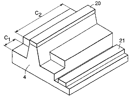
The semiconductor laser device of an embodiment
according to the present invention has a first waveguide
region C1 and a second waveguide region C2 as stripe
waveguide region as shown in Fig. 1A.
The first waveguide region C1 is a waveguide region
CA 02411445 2005-12-05
where a ridge (first ridge 201) is formed so as to include an
active layer 3. A difference in the refractive index of the
first waveguide region C1 is created between the active layer
3 and the regions (in the atmosphere in this case) located on
5 both sides thereof as shown in Fig. 1C, thereby to confine
light within the active layer 3. The waveguide region where
light is confined by providing an actual difference in the
refractive index between the active layer and the regions on
both sides thereof will be referred to as the total
10 refractive index type waveguide.
The second waveguide region C2 is a waveguide region
where a ridge (second ridge 202) is formed in the
semiconductor layer located on the active layer so that the
effective refractive index of the active layer 3 located
below the second ridge 202 is made higher than that of the
active layer located on both sides thereof as shown in Fig.
1B, thereby to confine light within the active layer 3 having
higher effective refractive index. The waveguide
region where light is confined by providing an
effective difference in the refractive index between the
active layer and the regions on both sides thereof will be
referred to as the effective refractive index type waveguide
The semiconductor laser according to the present
invention is characterized by the total refractive index type
waveguide and the effective refractive index type waveguide
provided in the waveguide.
Specifically, the second waveguide region C2 is
CA 02411445 2005-12-05
11
constituted by forming the laminate consisting of the layer
of the first conductivity type, the active layer and the
layer of the second conductivity type which is different from
the first conductivity type being stacked one on another, and
forming the second stripe ridge 202 on the layer 2 of the
second conductivity type to such a depth as the active layer
is not reached. The first waveguide region C1 is
constituted by forming the first stripe ridge 201 so as to
include portions of the layer 2 of the second conductivity
type, the active layer 3 and the layer 1 of the first
conductivity type.
By having the first waveguide region C1 and the second
waveguide region C2 in the waveguide as described above, semiconductor
laser devices of diverse characteristics can be obtained. The
waveguide having the first waveguide region C1 and the second
waveguide region C2 can be formed in various forms as shown
in Figs. 3 and 4. Fig. 3A is a partially cutaway perspective
view of the laser device of such a structure as the stripe
ridge is formed by removing a part of the laminate. Fig. 3B
is a cross section viewed in the direction of arrow in Fig.
3A. Figs. 4A and 4B show a waveguide structure different
from that shown in Fig. 3.
As shown in Figs. 3 and 4, various constitutions can be employed
where the first waveguide region C1 and the second waveguide region C2 are
CA 02411445 2005-12-05
12
disposed in various arrangements in the resonator direction
(longitudinal direction of the stripe ridge). The
semiconductor laser may also have a waveguide
region other than the first waveguide region C1
and the second waveguide region C2, as a matter of
fact. For example, a waveguide region 203 different from the
first waveguide region C1 and the second waveguide region C2
may be provided between the first waveguide region C1 and the
second waveguide region C2 as shown in Fig. 4A. Fig. 3 shows
such a structure'as the first waveguide region C1 is provided
so as to include one of the resonance end faces of the
resonator and the second waveguide region C2 is provided so
as to include the other resonance end face. Fig. 4A shows a
semiconductor laser device having such a structure as the
first ridge 201 which constitutes the first waveguide region
C1 and the second stripe ridge 202 which constitutes the
second waveguide region C2 are joined via a waveguide region
203 which is formed so as to incline with respect to the
vertical direction (perpendicular to the resonator direction).
Thus the first waveguide region C1 and the second waveguide
region C2 may be formed either substantially continuously in
the resonator direction as shown in Fig. 3 or with another
region being interposed therebetween as shown in Fig. 4A.
The width of the first ridge 201 and the width of the second
ridge 202 may not be substantially the same. For example, in
case the side face of each ridge is formed to incline as shown in
CA 02411445 2005-12-05
13
Figs. 1 and 3, width at the base of the first ridge 201
provided to constitute the first waveguide region C1 and
width at the base of the second ridge 202 provided to
constitute the second waveguide region C2 become inevitably
different from each other. The side face of the first ridge
and the side face of the second ridge preferably lie in the
same plane. While the stripe ridges shown in Fig. 1 and Fig.
3 are formed in the normal mesa configuration where the side
faces are inclined so that width decreases from the base to
the top, the ridge may also be formed in the inverted mesa
configuration where the width increases from the base to the
top, and further both side faces of the mesa may be inclined
either in the same way or in the opposite manner.
Width of the top surface of the first ridge 201 and
width of the top surface of the second ridge 202 may be
different from each other. Further, width of the first ridge
201 and width of the second ridge 202 viewed in the
horizontal section may be different so as to change
discontinuously at the border of the first ridge 201 and the
second ridge 202.
[Resonator structure]
In the semiconductor laser device of this embodiment,
the stripe waveguide is constituted by removing a part of the
laminate structure and forming the ridge. That is, as shown
in Figs. 1 and 3, the resonator has such a structure as the
stripe ridge is formed by removing both sides of a portion
which would become the ridge by etching or other means in the
CA 02411445 2005-12-05
14
laminate consisting of the layer 1 of the first conductivity
type, the active layer 3 and the layer 2 of the second
conductivity type, which is suited to the so-called ridge
waveguide laser device. Since at least the
first waveguide region C1 and the second waveguide
region C2 are provided by means of the stripe ridge,
beam characteristic can be improved and particularly F.F.P.
can be controlled in a desired shape from ellipse to true
circle, so that various laser devices having diverse
characteristics can be provided. The stripe ridge is not
limited to the normal mesa configuration shown in Figs. 1 and
3 as described above, and may be formed in inverted mesa
configuration or in stripe shape having vertical side faces.
That is, the ridge shape may be changed according to the
laser characteristic required.
Also in the semiconductor laser device, the
ridge may be buried by regrowing crystal on both sides
of the ridge after forming the stripe ridges 201,
202 when constituting the first waveguide region C1 and the
second waveguide region C2.
As described above, since it is assumed that the
ridge waveguide structure has the stripe ridge, it is
possible not only to achieve production at a lower cost
but also to make laser devices with diverse characteristics
by arranging the first waveguide region C1 and the second
waveguide region C2 in various combinations in the waveguide.
For example, since it is made possible to control the beam
CA 02411445 2005-12-05
characteristic, satisfactory F.F.P. can be achieved without
using beam correction lens or the like.
In the laser device, the first and second stripe
ridges 201, 202 provided in the first waveguide
5 region C1 and the second waveguide region C2 have
such a configuration as shown in Fig. 1B and Fig. 1C.
The present invention is also applicable to devices
other than laser oscillation device, for example end-face
light emitting devices such as light emitting diode. The
10 device having the constitution shown in Fig. 1 can be
operated as a light emitting diode by driving the device
below the threshold of oscillation, and a device which emits
light from an end face without laser oscillation can be
obtained by inclining the waveguide from the direction which
15 is perpendicular to the end face, rather than making the
waveguide perpendicular to the end face.
[Laminate structure]
Now the structure of the laminate consisting of the
layer of first conductivity type, the active layer and the
layer of second conductivity type provided in the
semiconductor device of this embodiment will be described in
detail below.
In the semiconductor device of this embodiment, as shown
in Fig. 1, cladding layers 5, 7 are provided in the layer 1
of first conductivity type and the layer 2 of second
conductivity type, respectively, and light is confined in the
direction of thickness by sandwiching the active layer 3 with
CA 02411445 2005-12-05
16
the cladding layers 5, 7. Thus the optical waveguide region
is provided within the laminate where light is confined in
the width direction (perpendicular to the direction of
thickness and perpendicular to the direction of resonance) by
means of ridge and also light is confined in the direction of
thickness by means of the cladding layers 5, 7. In the
semiconductor laser device, various kinds of
semiconductor material known in the prior art can be
used such as those based on, for example, GaAlAs, InGaAsP and
GaAlInN.
In the semiconductor laser device, the
stripe waveguide region is formed in correspondence
to the ridge in the active layer between the
layer of the first conductivity type and the layer of the
second conductivity type, and in the vicinity thereof, while
the longitudinal direction of the stripe and the direction of
light propagation are substantially identical. That is,
while the stripe waveguide region is constituted mainly from
the active layer in which light is confined, part of light is
guided while spreading in the vicinity thereof, and therefore
a guide layer may be formed between the active layer and the
cladding layer so that the region including the guide layer
is used as the optical waveguide layer.
[Second waveguide region C2]
The second waveguide region C2, is a region
provided as the effective refractive index type
waveguide in the waveguide of the semiconductor laser device.
CA 02411445 2005-12-05
17
Specifically, the stripe ridge 201 is formed in the layer 2
of second conductivity type 2 located on the active layer 3
of the laminate, and the stripe waveguide region is formed by
providing effective difference in refractive index in the
direction of plane (width direction) of the active layer.
In a laser device of effective refractive index type of
the prior art in which the waveguide consists of the second
waveguide region C2 only, the stripe ridge 202 is formed by
etching using a mask 20 after forming the semiconductor
layers as shown in Fig. 2. Since the stripe ridge 202 is
formed by etching to such a depth that does not reach the
active layer thereby to provide the effective difference in
refractive index in the active layer (waveguide layer),
characteristics of the device vary significantly depending on
the width Sw of the stripe, height of the ridge (depth of
stripe) Sh, and distance Sh2 between the surface exposed by
etching and the top plane of the active layer as shown in Fig.
2B. These factors cause serious variations in the device
characteristics during production. That is, the
variations in the device characteristics are caused directly
by error Hd in the height of the ridge (depth of stripe) and
error Wd in the width of the stripe related to the accuracy
of etching shown in Fig. 2C and Fig. 2D. This is because the
waveguide region formed in the active layer (waveguide layer)
is provided by making use of the effective difference in
refractive index corresponding to the ridge 202 by means of
the stripe ridge 202 provided in the active layer (waveguide
CA 02411445 2005-12-05
18
layer), and therefore the configuration of the ridge has a
significant influence on the effective difference in
refractive index . The error Hd in the height of the ridge
is also the error in the distance between the surface exposed
by etching and the top plane of the active layer. When the
distance Sh2 between the top plane of the active layer and
the surface exposed by etching is too large, the effective
difference in refractive index becomes smaller resulting in
significant influences on the device characteristics such as
insufficient confinement of light. As described above, since
the effective refractive index is dependent on the distance
Sh2 between the top plane of the active layer and the surface
exposed by etching, variations in the distance cause
variations in the effective refractive index.
Figs. 10, 11 and 12 show the ratio of products which
pass the etching depth inspection, drive current and service
life for the laser device of the effective refractive index
type of the prior art. As will be understood from the
drawings, characteristics of the laser device are very
sensitive to the depth of.etching.
In the laser device, since the second
waveguide region C2 formed by etching to such a depth
that does not reach the active layer is provided as a part of
the waveguide, the active layer is prevented from being
damaged by etching in the second waveguide region C2, and
therefore reliability of the device can be improved. In the
case of a material which undergoes significant device
CA 02411445 2005-12-05
19
characteristics when the active layer is exposed to the
atmosphere, providing the second waveguide region C2 makes it
possible to restrict the reliability of the device from
deteriorating.
[First waveguide region C1]
Laser devices of various characteristics
can be easily made by forming the first waveguide
region C1 in addition to the second waveguide
region C2 as the stripe waveguide region, as described
previously. This is an effect brought about by the excellent
controllability of the transverse mode of the first waveguide
region C1 which is made by forming the stripe ridge 201 that
includes portions of the active layer and the layer 1 of the
first conductivity type in the laminate structure.
In the first waveguide region C1, since light is
confined by means of the actual difference 'in the refractive
index between the active layer and the regions located on
both sides thereof by limiting the width of the active layer
by the first ridge, it is made possible to confine light more
effectively.
Thus it is made possible to surely suppress the
unnecessary transverse mode of oscillation and control the
transverse mode more effectively.
As described above, by providing the first
waveguide region C1 having excellent controllability
of transverse mode in a part of the waveguide
region, unnecessary transverse mode of oscillation in the
CA 02411445 2005-12-05
first waveguide region C1 is suppressed thereby improving the
controllability of transverse mode of the entire device, and
it is made possible to easily obtain laser devices of various
beam characteristics.
5 With the laser device, laser beam of a desired
configuration can be easily achieved by forming
the first waveguide region C1 on one end so as to
include the resonance end face of the laser resonator. In
other words, it is preferable to form the laser resonance end
10 face 4 so as to correspond to the end face of the first
waveguide region C1 as shown in Fig. 3B, Fig. 4A and Fig. 4B.
When the region in the vicinity of the resonance
end face is turned into the first waveguide region
C1, the transverse mode of light can be controlled before and
15 after reflection on the resonance end face, so that the
control of the transverse mode functions more effectively in
the waveguide than.in a case of providing in other region
The laser device having excellent beam
characteristics such as F.F.P. and laser beam
20 aspect ratio can be obtained by using the end
face of the first waveguide region C1 as the laser resonance
end -face and using the laser resonance end face as the light
emitting plane. This is because, with this constitution, by
providing the first waveguide region C1 on the laser beam
emitting plane. With this constitution, by providing
the first waveguide region C1 on the laser beam
emitting plane, it is easier to control the transverse
CA 02411445 2005-12-05
21
waveguide region C1 is constituted from the first stripe
ridge 201 as shown in Figs. 3, 4, the transverse mode can be
easily controlled and the desired beam characteristic can be
obtained with high accuracy by adjusting the width of stripe
of the first ridge 201.
Length of the first waveguide region C1 provided on the
light emitting plane may be at least one wavelength of the
light emitted by the laser, though a length of several times
the wavelength is preferable in consideration of the function
to control the transverse oscillation mode in which case
desired beam characteristic can be achieved.
Specifically, it is preferable to form the first
waveguide region C1 with a length of 1 m or longer, which
enables satisfactory control of the transverse oscillation
mode. When consideration is given to the manufacturing
process, it is preferable to form the first waveguide region
with a length of 5 g m or longer since the stripe ridge 201
can be formed with better accuracy with this length.
Width of the active layer (length in the direction
perpendicular to the resonator direction) may be 10 p m,
preferably 50 m or longer and more preferably 100 p m or
longer. In such a constitution as a pair of positive and
negative electrodes oppose each other via a substrate, width
of the active layer becomes equivalent to the chip width. In
such a constitution as a pair of positive and negative
electrodes is provided on the same side of a substrate, a
surface is exposed to form electrodes in the layer of the
CA 02411445 2005-12-05
22
first conductivity type thereon, the length is the chip width
minus the width of the portion which is removed to form the
exposed surface.
[Constitution of waveguide]
The laser device is characterized by the
stripe waveguide region having at least the first
waveguide region C1 and the second waveguide region
C21 so that the characteristics of the laser devices can be
easily modified by changing the arrangement of the waveguide
regions in the resonator without device design
modification. Specifically, by disposing the first
waveguide region C1 on the resonance end face as
described above, beam characteristic can be easily controlled
and desired characteristic can be easily obtained. Also by
setting the proportion of the waveguide occupied by the first
waveguide region C1 wherein the side face of the active layer
is exposed smaller than that of the second waveguide region
C21 the laser device of higher reliability can be obtained.
This is because the proportion of the active layer which is
not damaged by etching can be increased by providing more
second waveguide region C2 in the waveguide. As a result,
service life of the device can be elongated and variations in
the service life among the devices can be decreased.
While the laser device has at least the
first waveguide region C1 and the second waveguide
region C2 as the waveguide, a waveguide region of a
configuration other than the first waveguide region C1 and
CA 02411445 2005-12-05
23
the second waveguide region C2 may also be provided. For
example, a flat surface 203 formed to incline between the
first waveguide region C1 and the second waveguide region C2
as shown in Fig. 4A may be used. Thus in addition to the
first waveguide region C1 and the second waveguide region C21
a waveguide different from these may be provided. Further,
the first waveguide region C1 and the second waveguide region
C2 may be provided, one each, in the waveguide or may be
provided in plurality as shown in Fig. 4B. Also nothing may
be provided between the first waveguide region C1 and the
second waveguide region C2 as shown in Fig. 3 and Fig. 4B, or
an inclination reverse to that shown in Fig. 4A may be
provided so that the first waveguide region C1 and the second
waveguide region C2 partially overlap each other.
The laser device may also have a third
waveguide region C3 formed in addition to the
first waveguide region Cz with the second waveguide
region C2 so that the side face of the active layer
(side face of waveguide layer) 204 inclined against the
resonator direction. Fig. 13A is a schematic perspective
view of the device structure, and Fig. 13B is a sectional
view showing a portion near the junction between the upper
cladding layer 7 and the active layer 3. In this
constitution, the third waveguide region C3 shares the stripe
ridge 202 on the upper cladding layer 7 with the second
waveguide region C2, and the end face (side face) 204 of the
active layer (waveguide layer) is provided in an inclined
CA 02411445 2005-12-05
24
configuration. In the laser device having the constitution
described above, light guided by the side face 204 can be
reflected completely by adjusting the angle a between the
resonator direction AA and the direction BB of the active
layer side face, as shown in Fig. 13B, thus making it
possible to guide the light into the first waveguide region
C1 first waveguide region C1 striped configuration.
Specifically, when the angle a is 70 or less, the incident
angle of light in the direction AA of the resonator on the
end face 204 can be set to 20 or greater so that total
reflection without loss can be achieved. Thus the angle a
can be set in a range from 0 to 70 according to the
application. For example, when the angle a is 20 or less,
the incident angle of light in the direction AA of the
resonator on the end face 204 can be set to 70 or greater,
in which case total reflection without loss can be achieved.
In the second waveguide region C21 while-the stripe waveguide
region is formed by making use of the effective difference in
refractive index in the active layer (waveguide layer), there
exists light tat is guided outside of the waveguide region
and this portion of light is reflected on the end face of the
second waveguide region C2.
In this case, when the loss in light increases, output
power decreases leading to a deterioration in the current-
optical output slope efficiency. When the second waveguide
region C2 is wider than the first waveguide region C1,
providing the third waveguide region C3 between the second
CA 02411445 2005-12-05
waveguide region C2 and the first waveguide region C1
decreases the light loss, thus making it possible to guide
the light satisfactorily in the junction with the first
waveguide region C1 as shown in Fig. 13.
5 In the laser device, the stripe ridges 201,
202 that constitute the first waveguide region C1
and the second waveguide region C2 may have different widths.
Beams of different aspect ratios can be achieved by changing
the stripe width. Therefore, the first ridge and the second
10 ridge can be formed with widths appropriate for the
application in the laser device accurate. While
a small width requires the control of the
width, it also achieves such characteristics
as FFP near true circle or changes in the spread of
15 the beam in correspondence to the width. Specifically, when
the width is decreased gradually in a portion 205 of the
second waveguide region C2 as shown in Fig. 15, for example,
the stripe width in the junction with the first waveguide
region C1 can be made equal to the stripe width Sw2, thus
20 making it possible to extract laser beam of various modes in
correspondence to the width of the first waveguide region C1.
In Fig. 15, a portion where width of the second waveguide
region C2 is decreased gradually is shown as the third
waveguide region C3.
25 In Fig. 15, in order to constitute the second waveguide
region C2, the first ridge 202 having width Swl larger than
the stripe width Sw2 of the first ridge that constitutes the
CA 02411445 2005-12-05
26
first waveguide region C1 is provided thereby to form a
waveguide which undergoes less variation in the
characteristic with a change in the effective refractive
index. In the third waveguide region C3, at the same time, a
region 205 having stripe width inclined in the waveguide is
provided so as to join the waveguide regions of different
stripe widths smoothly, thereby minimizing the loss in the
junction. The ridge for constituting the third waveguide
region C3 may be provided above the active layer as shown in
the drawing, or at a depth reaching the layer of first
conductivity by etching similarly to the first waveguide
region C1, or at a position located inbetween.
The stripe ridge for constituting the first and second
waveguide regions may be formed in various
configurations, for example in a tapered
configuration where the stripe width varies along the
direction of stripe (longitudinal direction of stripe).
Specifically, as exemplified by the first embodiment or shown
in Fig. 15, in the waveguide structure having the first
waveguide region. C1 disposed at the light emitting end, the
second waveguide.region C2 having larger stripe width may be
formed in such a configuration that the stripe width
decreases toward the narrower first waveguide region C1,
thereby decreasing the light waveguide to the junction of
both portions. Such a tapered stripe may be formed partially
as the stripe of each waveguide region, or formed in a
tapered configuration over the entire length of the stripe,
CA 02411445 2005-12-05
27
or in such a configuration as a plurality of tapered stripes
having width which decreases toward both ends thereof.
[Stripe in nitride semiconductor]
The semiconductor laser device constituted
from the semiconductors of the first conductivity
type and the second conductivity type and the active layer
made of nitride semiconductor will be described below.
The nitride semiconductor used in the laser
device may be GaN, A1N or InN, or a mixed crystal
thereof, namely the Group III-V nitride semiconductor
(InbAldGal-b-dN, 0 5 b, 0 < d, b + d < 1) . Mixed crystals
made by using B as the Group III element or by partially
replacing N of the Group V element with As or P may also be
used. The nitride semiconductor can be made to have a
desired conductivity type by adding an impurity of
appropriate conductivity type. As an n-type impurity used in
the nitride semiconductor, the Group IV or VI elements such
as Si, Ge, Sn, S, 0, Ti and Zr may be used, while Si, Ge or
Sn is preferable and most preferably Si is used. As the p-
type impurity, Be, Zn, Mn, Cr, Mg, Ca or the like may be used,
and Mg is preferably used. As a specific example of the
laser device, a nitride semiconductor laser
device will be described below. The nitride
semiconductor laser device herein refers to a laser
device where nitride semiconductor is used in any of the
layer of the first conductivity type, the active layer and
the layer of the second conductivity type which constitute
CA 02411445 2005-12-05
28
the laminate, or preferably in all of these layers. For
example, cladding layers made of nitride semiconductor are
formed in the layer of the first conductivity type and the
layer of the second conductivity type while the active layer
is formed between the two cladding layers thereby forming the
waveguide. More specifically, the layer of the first
conductivity type includes a n-type nitride semiconductor
layer and the layer of the second conductivity type includes
a p-type nitride semiconductor layer, while the active layer
includes nitride semiconductor laser which includes In.
(Active layer)
When the semiconductor laser device is constituted
from nitride semiconductor, providing the nitride
semiconductor layer which includes In in the active
layer enables emission of a laser beam over a range of
wavelengths from blue to red light in the ultraviolet and
visible regions. While the laser device may suffer very
damage on the nitride semiconductor laser including
In when the active layer is exposed to the atmosphere,
such a damage to the device can be minimized
according since the device includes the second
waveguide region C2 constituted from the first ridge
202 provided at such a depth that does not reach the active
layer. This is because the low melting point of In makes the
nitride semiconductor including In decompose and evaporate
easily and prone to damage during etching, making it
CA 02411445 2005-12-05
29
difficult to maintain the crystallinity during the process
following the exposure of the active layer, thus resulting in
a shorter service life of the device.
Fig. 12 shows the relationship between the depth of
etching for forming the stripe ridge and the device life. As
will be seen from the drawing, device life decreases
dramatically when etching process reaches the active layer
which has the nitride semiconductor which includes In, and
exposure of the active layer leads to serious deterioration
of the reliability of the laser device.
Since the laser device is provided with
the first waveguide region C1 and the second
waveguide region C2 as the waveguide, the laser device of
excellent reliability can be achieved even in a nitride
semiconductor laser device which would otherwise undergo
deterioration in the characteristics when the active layer is
exposed to the atmosphere. This is because the first ridge
201 provided for the constitution of the first waveguide
region C1 constitutes only a part of the waveguide so that
reliability of the device can be prevented from deteriorating.
When length of the resonator is set to about 650 g m and
length of the first ridge 201 provided for the constitution
of the first waveguide region C1 is set to 10 m in the
nitride semiconductor laser device, for example,
it is confirmed that the device does not undergo
deterioration in reliability due to the active layer being
exposed in the first ridge, and service life of several
CA 02411445 2005-12-05
thousands of hours is ensured with operation of 5 mW in
output power.
In the nitride semiconductor laser device,
width of the stripe of the ridge that constitutes
5 the first waveguide region C1 or the second waveguide region
C2 is preferably set in a range from 0.5 to 4 u m, or more
preferably in a range from 1 to 3 m in which case it is
made possible to oscillate in stable transverse mode with the
fundamental (single) mode. When stripe width of the ridge is
10 less than 1 g m, it becomes difficult to form the ridge,
while width of 3 u m or greater may cause multi-mode
oscillation in the transverse mode depending on the
wavelength of laser oscillation, and width of 4 u m or
greater may make it impossible to achieve stable transverse
15 mode. Controlling the width in a range from
1.2 to 2 p m enables further stabilization of,
the transverse mode in a high optical output
power (effectively suppressing the oscillation
in unnecessary transverse mode). While it
is good for the stripe width of the ridge
when either of the first waveguide region C1 or the second
waveguide region C2 is within the range described above, it
is preferable to set the stripe ridge 201 of the first
waveguide region C1 within the range described above in case
the first waveguide region C1 is provided on the light
emitting side of the resonator plane. Also the present
invention is not limited to such a narrow stripe structure as
CA 02411445 2005-12-05
31
described above, and may be applied to a stripe having a
width of 5 p m or greater. When the first
waveguide. region C1 is disposed on the end of the
waveguide, the stripe width of the second waveguide region C2
can be set relatively freely for the control of the laser
beam characteristic by means of the first waveguide region
C1.
In the nitride semiconductor laser device,
when the end face of the first waveguide. region C1
is used as the resonance end face (light emitting plane), the
laser device having improved controllability of transverse
mode, F.F.P. aspect ratio and device reliability can be
obtained. As described previously, light emitted
from the laser device can be controlled immediately
before the emission by etching deeper than the active layer
thereby providing the first waveguide region C1 on the light
emitting side of the resonator plane, thereby making it
possible to obtain laser beams of various shapes and spot
sizes.
The active layer may have quantum well structure and, in
that case, may be either a single quantum well or a multiple
quantum well structure. High power laser device and end face
light emitting device with good light emitting efficiency can
be made by employing the quantum well structure. The
second stripe ridge 202 constituting the second
waveguide region C2 is formed by etching to a depth that
does not reach the active layer. In this specification, the
CA 02411445 2005-12-05
32
statement that the second stripe ridge 202 is located above
the active layer means that the formation by etching to such
a depth that the etching does not reach the active layer. That is, the
second stripe ridge 202 that constitutes the second waveguide
region C2 is positioned above the interface between the
active layer and the layer formed in contact and above
thereof.
The active layer of the nitride semiconductor is
preferably the nitride semiconductor which includes In as
described above, and specifically a nitride semiconductor
represented by AlXInYGal_x_,,N (0 < x : 1, 0 < y < 1, x + y S
1) is preferably used. In this case, the nitride
semiconductor described here is preferably used as the well
layer in the active layer of quantum well structure. In the
wavelength region (from 380 nm to 550 nm) ranging from near
ultraviolet to visible green light, InYGal_YN (0 < y0) is
preferably used. Also in a region of longer wavelengths
(red), InYGa1-YN (0 < y0) can be used similarly and, at this
time, laser beam of a desired wavelength can be emitted by
changing the proportion y of mixing In. In a region of
wavelengths shorter than 380 nm, since the wavelength which
corresponds to the forbidding band width of GaN is 365 nm,
band gap energy nearly equal to or greater than that of GaN
is required, and therefore Al InYGa1_x_YN (0 < x < 1, 0 < y
1, x + y < 1) is used.
In case the active layer is formed in the quantum well
structure, thickness of the well layer is in a range from 10
CA 02411445 2005-12-05
33
A to 300 A, and preferably in a range from 20 A to 200 A,
which allows it to decrease Vf and the threshold current
density. When the crystal is taken into consideration, a
layer of relatively homogeneous quality without much
variations in the thickness can be obtained when the
thickness is 20 A or greater, and the crystal can be grown
while minimizing the generation of crystal defects by
limiting the thickness within 200 A. There is no limitation
on the number of well layers in the active layer, which may
be 1 or more. When four or more active layers with larger
thickness of layers constituting the active layer, total
thickness of the active layers becomes too large and the
value of Vf increases. Therefore, it is desirable to
restrict the thickness of the well layer within 100 A thereby
to restrain the thickness of the active layer. In the case
of LD and LED of high output power, setting the number of
well layers in a range from 1 to 3 makes it possible to
obtained devices of high light emission efficiency and is
desirable.
The well layer may also be doped or undoped with p- or
n-type impurity (acceptor or donor). When nitride
semiconductor which includes In is used as the well layer,
however, increase in the concentration of n-type impurity
leads to lower crystallinity and therefore it is preferable
to restrict the concentration of n-type impurity thereby to
achieve make the well layer of good crystallinity.
Specifically, in order to achieve best crystallinity, the
CA 02411445 2005-12-05
34
well layer is preferably grown without doping with the n-type
impurity concentration kept within 5 X 10¹⁶/cm3. The state
of the n-type impurity concentration kept within 5 X 10¹⁶/cm3
means an extremely low level of concentration of n-type
impurity, and the well layer can be regarded as including
substantially no n-type impurity. When the well layer is
doped with n-type impurity, controlling the n-type impurity
concentration within a range from 1 X 10¹⁸/cm3 to 5 X 10¹⁶/cm3
makes it possible to suppress the degradation of
crystallinity and increase the carrier concentration.
There is no limitation to the composition of the barrier
layer, and nitride semiconductor similar to that of the well
layer can be used. Specifically, a nitride semiconductor
which includes In such as InGaN having lower proportion of In
than the well layer, or a nitride semiconductor which
includes Al such as GaN, AlGaN may be used. Band gap energy
of the barrier layer must be higher than that of the well
layer. Specific composition may be InpGal_8N (0 /3 < 1, a
> Q ), GaN, Al,,Ga1_,,N (0 < y < 1), and preferably InGGa,-,N
(0 8 < 1, a > 8 ), GaN which makes it possible to form
the barrier layer of good crystallinity. This is because
growing a well layer made of a nitride semiconductor which
includes In directly on a nitride semiconductor which
includes Al such as AlGaN leads to lower crystallinity,
eventually resulting in impeded function of the well layer.
When Al,,Gal_,,N (0 < y < 1) is used in the barrier layer, the
above problem can be avoided by providing the barrier layer
CA 02411445 2005-12-05
which includes Al on the well layer and providing a multi-
layered barrier layer comprising In5Gal_,,N (0 < 0 < 1, a >
/3), GaN below the well layer. Thus in the multiple quantum
well structure, the barrier layer sandwiched between the
5 active layers is not limited to a single layer (well
layer/barrier layer/well layer). Two or more barrier
layers of different compositions and/or impurity
concentrations may be stacked such as well layer/barrier
layer (1)/ barrier layer (2)/well layer. Letter a represents
10 the proportion of In in the well layer. It is preferable
to make the proportion of In 8 in the barrier layer lower
than that of the well layer as a > 8.
The barrier layer may be doped or undoped with the n-
type impurity, but preferably doped with the n-type impurity.
15 When doped, the n-type impurity concentration in the barrier
layer is preferably 5 X 10¹⁶/cm3 or higher and lower than 1
X 1020/cm3. In the case of LED which is not required to have
a high output power, for example, the n-type impurity
concentration is preferably in a range from 5 X 10¹⁶/cm3 to 2
20 X 1018/cm3. For LED of higher output power and LD, it is
preferable to dope in a range from 5 X 10¹⁷/cm3 to 1 X
1020/cm3 and more preferably in a range from 1 X 10¹⁸/cm3 to 5
X 1019/cm3. When doping to such a high concentration, it is
preferable to grow the well layer without doping or with
25 substantially no n-type impurity included. The reason for
the n-type impurity concentration being different among the
regular LED, the high-power LED and the high-power LD (output
CA 02411445 2005-12-05
36
power in a range from 5 to 100 mW) is that a device of high
output power requires higher carrier concentration in order
to drive with larger current for higher output power. Doping
in the range described above, as described above, it is made
possible to inject the carrier to a high concentration with
good crystallinity.
In the case of a nitride semiconductor device such as
lower-power LD, LED or the like, in contrast, a part of the
barrier layer of the active layer may be doped with the n-
type impurity or the entire barrier layers may be formed with
substantially no n-type impurity included. When doping with
the n-type impurity, all the barrier layers of the active
layer may be doped or a part of the barrier layers may be
doped. When part of the barrier layers is doped with the n-
type impurity, it is preferable to dope the barrier layer
which is disposed on the n-type layer side in the active
layer. Specifically, when the barrier layer Bn (n = 1, 2, 3
... ) which is nth layer from the n-type layer side, electrons
are effectively injected into the active layer and a device
having excellent light emission efficiency and quantum
efficiency can be made. This also applies to the well layer,
as well as the barrier layer. When both the barrier layer
and the active layer are doped, the effect described above
can be achieved by doping the barrier layer Bn (n = 1, 2, 3
... ) which is nth layer from the n-type layer side and the mth
well layer Wm (m = 1, 2, 3===), namely doping the layer nearer
to the n-type layer first.
CA 02411445 2005-12-05
37
While there is no limitation to the thickness of the
barrier layer, the thickness is preferably not larger than
500 A, and more specifically from 10 to 300 A similar to
the active layer.
In the nitride semiconductor laser device,
it is preferable that the laminate structure
includes the n-type nitride semiconductor layer for the layer
of first conductivity type and the p-type nitride
semiconductor for the layer of second conductivity type.
Specifically, the n-type cladding layer and the p-type
cladding layer are provided in the layers of the respective
types, thereby to form the waveguide. At this time, a guide
layer and/or an electron confinement layer may be formed
between the cladding layers and the active layer.
(p-type cladding layer)
In the nitride semiconductor laser device,
it is preferable to provide the p-type cladding
layer which includes the p-type nitride semiconductor (first
p-type nitride semiconductor) as the layer of second
conductivity type or the layer of first conductivity type.
In this case, the waveguide is formed in the laminate
structure by providing the n-type cladding layer which
includes the n-type nitride semiconductor layer in the layer
of the conductivity type different from that of the layer
wherein the p-type cladding layer is provided. The nitride
semiconductor used in the p-type cladding layer is required
only to have a difference in the refractive index large
CA 02411445 2005-12-05
38
enough to confine light, and nitride semiconductor layer
which includes Al is preferably used. This layer may be
either a single layer or a multi-layered film. Specifically,
a super lattice structure having AlGaN and GaN stacked one on
another achieves better crystallinity and is therefore
preferable. This layer may be either doped with p-type
impurity or not doped. For a laser device oscillating at a
long wavelength in a range from 430 to 550 nm, the cladding
layer is preferably made of GaN doped with p-type impurity.
While there is no limitation to the film thickness, thickness
in a range from 100 A to 2 gm, or more preferably from 500 A
to 1 gm makes the film function satisfactorily as the light
confinement layer.
The electron confinement layer and/or an optical
guide layer may be provided between the active layer and
the p-type cladding layer. When providing the optical
guide layer, the optical guide layer is preferably provided
between the n-type cladding layer and the active layer, in
such a structure as the active layer is sandwiched by optical
guide layers. This creates SCH structure in which light can
be confined by the cladding layer by making the proportion of
Al content higher in the cladding layer than in the guide
layer thereby providing a difference in refractive index. In
case the cladding layer and the guide layer are formed in
multi-layered structure, proportion of Al content is
determined by the mean proportion of Al.
CA 02411445 2005-12-05
39
(p-type electron confinement layer)
The p-type electron confinement layer which is provided
between the active layer and the p-type cladding layer, or
preferably between the active layer and the p-type optical
guide layer also function to confine the carrier in the
active layer thus making it easier to oscillate by reducing
the threshold current, and is made of AlGaN. More
effective electron confinement can be achieved by
providing the p-type cladding layer and the p-type electron
confinement layer in the layer of second conductivity type.
When AlGaN is used for the p-type electron confinement layer,
while the above mentioned function can be reliably achieved
by doping with the p-type impurity, carrier confining
function can also be achieved even without doping. Minimum
film thickness is 10 A and preferably 20 A. The above
mentioned function will be achieved satisfactorily by forming
the film to a thickness within 500 A and setting the value of
x in formula Al Ga1_xN to 0 or larger, preferably 0.2 or
larger. The n-type carrier confinement layer may also be
provided on the m-type layer side for confining the holes
within the active layer. Confinement of holes can be done
without making such an offset (difference in the band gap
from the active layer) as in the case of electron confinement.
Specifically, a composition similar to that of the p-type
electron confinement layer may be used. In order to achieve
good crystallinity, this layer may be formed from a nitride
semiconductor layer which does not includes Al, and a
CA 02411445 2005-12-05
composition similar to that of the barrier layer of the
active layer may be used. In this case, it is preferable to
dispose the n-type barrier layer which confines the carrier
nearest to the n-type layer in the active layer, or within
5 the n-type layer in contact with the active layer. Thus by
providing the p-type and n-type carrier confinement layers in
contact with the active layer, the carrier can be injected
effectively into the active layer or into the well layer. In
another form, a layer which makes contact with the p-type or
10 n-type layer in the active layer can be used as the carrier
confinement layer.
[p-type guide layer]
A waveguide can be formed from nitride
semiconductor by providing the guide layer which
15 sandwiches the active layer at a position inside
of the cladding layer thereby forming the optical waveguide.
In this case, thickness of the waveguide (the active layer
and the guide layers on both sides thereof) is set to within
6000 A for suppressing an abrupt increase in the oscillation
20 threshold current. Preferably the thickness is within 4500 A
to make continuous oscillation possible with long service
life at a restricted threshold current in the fundamental
mode. Both guide layers are preferably formed to
substantially the same thickness in a range from 100 A to 1
25 um, more preferably in a range from 500 A to 2000 A in order
to form good optical waveguide. The guide layer is made of
nitride semiconductor, while it suffices to have a band gap
CA 02411445 2005-12-05
41
energy sufficient to form the waveguide compared to the
cladding layer to be provided on the outside thereof, and may
be either a single film or a multi-layered film. Good
waveguide can be formed by making the optical guide layer
having a band gap energy equal to or greater than that of the
active layer. In the case of quantum well structure, band
gap energy is made greater than that of the well layer, and
preferably greater than that of the barrier layer. Further,
an optical waveguide can be formed by providing a band gap
energy for about 10 nm or larger than the wavelength of light
emitted in the active layer in the optical guide layer.
For the p-type guide layer, it is preferable to use
undoped GaN in the range of oscillation wavelengths from 370
to 470 rim, and use a multi-layered structure of InGaN/GaN in
a range of relatively long wavelengths (450 u m and over).
This makes it possible to increase the refractive index in
the waveguide constituted from the active layer and the
optical guide layer, thereby increasing the difference in the
refractive index from the cladding layer. In a range of
shorter wavelengths within 370 nm, nitride semiconductor
which includes Al is preferably used since the absorption
edge is at 365 nm. Specifically, Al.Gal_XN (0 < x < 1) is
preferably used to form a multi-layered film made of
AlGaN/GaN, multi-layered film made by alternate stacking
?5 thereof or a super lattice multi-layered film in which each
layer has super lattice structure. Constitution of the n-
type guide layer is similar to that of the p-type guide layer.
CA 02411445 2005-12-05
42
Satisfactory waveguide can be can be made by using GaN, InGaN
in consideration of the energy band gap of the active layer,
and forming multi-layered film comprising InGaN and GaN
stacked alternately with the proportion of In content being
decreased toward the active layer.
(n-type cladding layer)
In the nitride semiconductor laser device,
nitride semiconductor used in the n-type
cladding layer has a difference in the refractive
index large enough to confine light similarly to the p-type
cladding layer, and a nitride semiconductor layer which
includes Al is preferably used. This layer may be either a
single layer or a multi-layered film. Specifically, a super
lattice structure having AlGaN and GaN stacked one on another.
The n-type cladding layer functions as the carrier
confinement layer and the light confinement layer. In case
multi-layered structure is employed, it is preferable to grow
nitride semiconductor layer including Al, specifically AlGaN
as described previously. Further, this layer may be either
doped with n-type impurity or not doped, and also one of the
constituting layers may be doped. For a laser device
oscillating at a long wavelength in a range from 430 to 550
nm, the cladding layer is preferably made of GaN doped with
n-type impurity. While there is no limitation to the film
thickness, similarly to the case of the p-type cladding layer,
thickness in a range from 100 A to 2 um, or more preferably
from 500 A to 1 um makes the film function satisfactorily as
CA 02411445 2005-12-05
43
the light confinement layer.
In the nitride semiconductor laser device, good
insulation can be achieved by locating the position, where
the stripe ridge is formed, within the nitride semiconductor
layer which includes Al and providing an insulation film on
the exposed nitride semiconductor surface and on the side
face of the ridge. A laser device without leak current can
also be made by providing electrodes on the insulation film.
This is because almost no material exists that can achieve
good ohmic contact in the nitride semiconductor layer which
includes Al, and good insulation without leak current can be
achieved by forming the insulation film and electrode on the
semiconductor surface. When the electrode is provided on. the
nitride semiconductor layer which does not include Al, in
contrast, ohmic contact can be easily formed between the
electrode and the nitride semiconductor. When the electrode
is formed on the nitride semiconductor layer which does not
include Al via the insulation film, microscopic pores in the
insulation film cause leakage depending on the film quality
of the insulation film and the electrode. In order to solve
this problem, it is necessary to form the insulation film
having a thickness sufficient to provide the required level
of insulation or to design the shape and position of the
electrode so as not to overlap the semiconductor surface,
?5 thus imposing a significant restraint on the design of the
laser device constitution. It is important where to provide
the ridge, because the surface of the nitride semiconductor
CA 02411445 2005-12-05
44
on both sides of the ridge exposed when forming the ridge has
far greater area than the side face of the ridge, and
satisfactory insulation can be secured in this surface. Thus
a laser device having a high degree of freedom in the design
can be made where electrodes of various configurations can be
applied and the location of forming the electrode can be
determined relatively freely, which is very advantageous in
forming the ridge. For the nitride semiconductor layer which
includes Al, AlGaN or the super lattice multi-layered
structure of AlGaN/GaN described above is preferably used.
The first ridge 201 and the second stripe ridge 202 of
striped configuration provided as the first waveguide region
C1 and the second waveguide region C2 are formed by removing
both sides of each ridge as shown in Figs. 1B and 1C. The
ridge 202 is provided on the upper cladding layer 7 and the
surface of the upper cladding layer 7 exposed in a region
other than the ridge determines the depth of etching.
[Electrode]
The laser device is not limited to the
electrode configuration provided on the stripe ridge
and the second ridge. As shown in Fig. 1 and Fig. 7, for
example, the electrode may be formed on almost the entire
surface of the first stripe ridge 201. and the second stripe
ridge 202 provided as the first waveguide region C1 and the
second waveguide region C2. Also the electrode may be
provided on the second waveguide region C2 only thereby
injecting the carrier into the second waveguide region C2
CA 02411445 2005-12-05
with preference. On the contrary, the electrode may be
provided on the first waveguide region C1 only, with the
waveguide being functionally separated in the direction of
resonator.
5 [Insulation film]
In the laser device, in case a part of
the laminate is removed and a stripe ridge is
provided to form the resonator, it is preferable to form the
insulation film on the side face of the stripe and on the
10 plane (surface whereon the ridge is provided) on both sides
of the ridge which continues thereto. For example, after the
stripe ridge shown in Fig. 1 is provided, the insulation film
is provided in such a way as to extend from the side face of
the ridge to the surfaces on both sides of the ridge.
15 In case nitride semiconductor is used in the laser
device, it is preferable to provide a second protective film
162 as an insulation film as shown in Figs. 7, 8, 9.
For the second protective film, a material other than
20 S'021 preferably an oxide which includes at least one kind of
element selected from among the group consisting of Ti, V, Zr,
Nb, Hf and Ta, or at least one of SiN, BN, SiC and AlN is
used and, among these, it is particularly preferable to use
Zr or Hf, or BN, SiC. While some of these materials are
?5 slightly soluble to hydrofluoric acid, use of these materials
as the insulation layer of the laser device will achieve
reliability fairly higher than S'02 as a buried layer. In
CA 02411445 2005-12-05
46
the case of a thin film made of an oxide which is formed in
vapor phase such as PVD or CVD, since it is generally
difficult for the element and oxygen to react
stoichiometrically.to form the oxide, reliability tends to be
lower for the insulation of the thin film of oxide. In
contrast, oxides of the element selected in the present
invention formed by PVD or CVD, and BN, SiC or A1N have
higher reliability of insulation property than Si oxide.
Moreover, when an oxide having a refractive index lower than
that of the nitride semiconductor (for example, one other
than SiC) is selected, a buried layer of laser device can be
favorably formed. Further, when the first protective film
161 is formed from Si oxide, since the Si oxide can be
removed using hydrofluoric acid, the second protective film
162 having uniform thickness can be formed on the surface
except for the top surface of the ridge as shown in Fig. 7C,
by forming the first protective film 161 only on the top
surface of the ridge as shown in Fig. 7B, forming the second
protective film 162 continuously on the first protective film
161, the side faces of the ridge and the surfaces on both
sides of the ridge (etching stopper layer), and selectively
removing the first protective film 161.
Thickness of the second protective film is in a range
from 500 A to 1 am, and preferably in a range from 1000 A to
5000 A. When the thickness is less than 500 A, sufficient
insulation cannot be achieved when forming the electrode.
When thicker than 1 in, uniformity of the protective film
CA 02411445 2005-12-05
47
cannot be achieved and good insulation film cannot be
obtained. When the thickness is in the preferred range
described above, a uniform film having a favorable difference
in refractive index from that of the ridge can be formed on
the side face of the ridge.
The second protective film can also be formed by means
of buried layer of nitride semiconductor. In the case of
semi-insulating, i-type nitride semiconductor, type of
conductivity opposite to that of the ridge of the waveguide
region, for example in the second waveguide region C2 of the
first embodiment, a buried layer made of n-type nitride
semiconductor can be used as the second protective film. As
a specific example of buried layer, confinement of light in
the transverse direction can be achieved by providing a
difference in refractive index from the ridge by means of a
nitride semiconductor layer which includes Al such as AlGaN
or achieving the function of current blocking layer. A
laser device with good optical properties can be achieved by
providing a difference in the light absorption coefficient by
means of a nitride semiconductor laser which includes In.
When a layer other than semi-insulating, i-type layer is used
for the buried layer, the second waveguide region may be a
buried layer of the first conductivity type different from
the second conductivity type. In the first ridge that
constitutes the first waveguide region, since the
layers of the first and second conductivity types
are formed in stripe configuration on both sides of the
CA 02411445 2005-12-05
48
active layer, a buried layer of the second conductivity type
different from the first conductivity type is formed in the
layer of the first conductivity type or in the regions on
both sides of the layer of the first conductivity type and
the active layer, while a buried layer of the first
conductivity type different from the second conductivity type
is formed in the layer of the second conductivity type or in
the regions on both sides of the layer of the second
conductivity type and the active layer. As described above,
the buried layer may be formed in different constitutions in
the first waveguide region and the second waveguide region.
The buried layer is formed on a part of the stripe side face,
or preferably over substantially the entire surface,
similar to the second protective film. Moreover, when the
buried layer is formed on the side face of the ridge and the
surface of the nitride semiconductor on both sides of the
ridge, better light confinement effect and current pinching
effect can be achieved. Such a constitution may also be
employed as, after forming the buried layer, a layer of
nitride semiconductor is formed on the buried layer and/or
the stripe and ridges constituting the waveguide regions are
disposed in the device.
Length of the resonator of the nitride semiconductor
laser device of the present invention may be in a range from
400 to 900 u m, in which case the drive current can be
decreased by controlling the reflectance of the mirrors on
both ends.
CA 02411445 2005-12-05
49
[Manufacturing method]
The stripe waveguide region of the laser
device can be made with a high accuracy and
high yield of production, by forming the stripes
that make the first waveguide region C1 and the second
waveguide region C2 in the process described below. The
manufacturing method also makes it possible to manufacture
the laser device having high reliability. The manufacturing
method will now be described in detail below.
As shown in Figs. 8 and 9, when manufacturing a device
having a pair of positive and negative electrodes formed on
the same side of different kind of substrate, in order to
L5 expose an n-type contact layer whereon the negative electrode
is to be formed as shown in Fig. 7, etching is done to a specific
depth followed by etching to form the stripe waveguide region.
(Method 1 for forming the stripe ridge)
Fig. 5 is a schematic perspective view showing a part of
?0 a wafer whereon device structure is formed from nitride
semiconductor, for explaining the process of forming the
electrodes according to the present invention. Fig. 6 is a
similar drawing for explaining another embodiment of the
present invention. Fig. 7 shows a process after forming the
second protective film, Fig. 7B showing sectional view of the
second waveguide region C2 in Fig. 7A and Fig. 7C showing
sectional view of the second waveguide region C2 in Fig. 7D.
CA 02411445 2005-12-05
According to the manufacturing method shown
in Fig. 5A, after stacking the semiconductor
layers that constitute the device structure,
the first protective film 161 of stripe configuration is
5 formed on a contact layer 8 in the layer of second
conductivity type on the top layer.
The first protective film 161 may be made of any
material as long as it has'a difference from the etching rate
of the nitride semiconductor, whether insulating or not. For
10 example, Si oxide (including Si02)1 photoresist or the like
is used, and such a material that is more soluble to an acid
than the second protective film does is preferably used in
order to differentiate the solubility against the second
protective film which will be formed later. Hydrofluoric
15 acid is preferably used for the acid, and accordingly Si
oxide is preferably used as the material soluble to
hydrofluoric acid. Stripe width (W) of the first protective
film is controlled within a range from 1 g m to 3 u m.
Stripe width of the first protective film 161 roughly
20 corresponds to the stripe width of the ridge that constitutes
the waveguide region.
Fig. 5A shows the first protective film 161 being formed
on the surface of the laminate. That is, the first
protective film 161 having such a stripe configuration as
?5 shown in Fig. 5A is formed on the surface of the contact
layer 8 by, after forming the second protective film over
substantially the entire surface of the laminate, forming a
CA 02411445 2005-12-05
51
mask of a desired shape on the surface of the first
protective film by photolithography process.
Lift-off method may also be employed to form the first
protective film 161 having such a stripe configuration as
shown in Fig. 5A. That is, after forming a photoresist
having slits formed in stripe configuration, the first
protective film is formed over the entire surface of the
photoresist, and the photoresist is removed by dissolving
thereby leaving only the first protective film 161 which is
in contact with the contact layer 8. Well-shaped stripes
having substantially vertical end faces can be obtained by
the etching process described above rather than by forming
the first protective film of stripe configuration by the
lift-off method.
Then as shown in Fig. 5B, the first protective film 161
is used as the mask for etching from the contact layer 8 the
portion where the first protective film 161 is not formed,
thereby to form the stripe ridge according to the shape of
the protective film directly below the first protective film
161. When etching, structure and characteristic of the laser
device vary depending on the position to stop etching.
As the means for etching the layer formed from nitride
semiconductor, dry etching is used such as RIE (reactive ion
etching). For etching the first protective film made of Si
oxide, it is preferable to use gas of fluorine compound such
as CF4. For etching the nitride semiconductor in the second
process, use of gas of chlorine compound such as Cl., CC14
CA 02411445 2005-12-05
52
and SiCl4 which are commonly used for the other Group III-V
compound semiconductor makes the selectivity with respect to
the Si oxide higher, and is therefore desirable.
Then as shown in Fig. 5C, a third protective film 163 is
formed so as to cover a part of the stripe ridge. For the
third protective film 163, known resist film which has
resistance to dry etching can be used, such as light-
hardening resin. At this time, the stripe ridge covered by
the third protective film 163 becomes the second ridge 202
for constituting the second waveguide region C2, and the
first ridge 201 which constitutes the first waveguide region
C, is formed in a region not covered by third protective film.
The third protective film 163 and the first protective film
161 formed as described above are used to etch the laminate,
where the masks are not formed, to such a depth as to reach
the cladding layer, thereby to form the stripe ridges (first
ridge) of different depths.
Then as shown in Fig. 7A, the second protective film 162
of an insulating material different from that of the first
protective film 161 is formed on the side faces of the stripe
ridge and on the surfaces of the layers which have been
exposed by etching (cladding layers 5, 7 in Fig. 7) . The
first protective film 161 is made of a material different
from that of the second protective film 162, so that the
first protective film 161 and the second protective film 162
are selectively etching. As a result, when only the first
protective film 161 is removed by, for example, hydrofluoric
CA 02411445 2005-12-05
53
acid, the second protective film 162 can be formed
continuously over the surfaces of the cladding layers 5, 7
(the surfaces of the nitride semiconductor which have been
exposed by etching) and the side faces of the ridge with the
top surface of the ridge being opened as shown in Fig. 7B.
By forming the second protective film 162 continuously as
described above, high insulation property can be maintained.
In addition, when the second protective film 162 is formed
continuously over the first protective film 161, the film can
be formed with uniform thickness on the cladding layers 5, 7,
and therefore current concentration due to uneven film
thickness does not occur. Since the etching is stopped amid
the cladding layers 5, 7, the second protective film 162 is
formed below the surfaces of the cladding layers 5, 7 (top
surfaces which are exposed). However, the second protective
film is formed on the layer where the etching was stopped
when the etching is stopped below the cladding layers 5, 7,
as a matter of fact.
In the next process, the first protective film 161 is
removed by lift-off as shown in Fig. 7B. Then the electrode
is formed on the second protective film 162 and the contact
layer 8 so as to electrically contact the contact layer 8.
Since the second protective film having the striped openings
is formed first on the ridge, it is not necessary to form
the electrode only on the contact layer of narrow stripe
width, and the electrode is formed of a large area which
CA 02411445 2005-12-05
54
continues from the contact layer that is exposed through the
opening to the second insulation film. This makes it
possible to form the electrode combining the electrode for
ohmic contact and the electrode for bonding together, by
selecting the electrode material that combines the function
of ohmic contact.
When forming the stripe waveguide region in the nitride
semiconductor laser device, dry etching is employed because
it is difficult to etch by the wet process. Since
selectivity between the first protective film and the nitride
semiconductor is important in the dry etching process, SiO2
is used for the first protective film. However, sufficient
insulation cannot be achieved when S'02 is used also in the
second protective film formed on the top surface of the layer
where etching has been stopped, and the material is the same
as that of the first protective film, it becomes difficult to
remove the protective film only. For this reason, a material
other than S'02 is used for the second protective film
thereby ensuring the selectivity with respect to the first
protective film. Also because the nitride semiconductor
is not etched after forming the second protective
film, difference in the etching rate between the
second protective film and the nitride semiconductor makes no
problem.
(Method 2 for forming the stripe ridge)
Fig. 16 is a schematic perspective view showing a part
of a wafer whereon device structure is formed from nitride
CA 02411445 2005-12-05
semiconductor, for explaining the process of forming the
semiconductor laser. Processes of this method
are substantially similar to the processes of
the method 1, although the end faces of the
5 resonator are formed at the same time the n-type contact
layer is exposed for forming the negative electrode by
etching in the case of this method. Namely, the order of
forming different portions is different from the method 1.
In the method 2, first the n-type contact layer is exposed
10 (Fig. 16A) At this time, the end faces of the resonator are
formed at the same time. Then the stripe ridge, the first
and second waveguide regions and the electrode are formed
similarly to the method 1 (Fig. 16B). By forming the end
faces of the resonator by etching first as described above,
15 the invention can also be applied to such a case as good end
faces of the resonator cannot be obtained by cleaving.
In the laser device, as described above, the
stripe ridge 202 for constituting the first
waveguide region C1 and the second waveguide region C2
20 can be efficiently formed, and the electrode can be formed on
the surface of the ridge of the laminate.
(Etching means)
According to the manufacturing method, when dry
etching is used such as RIE (reactive ion etching)
25 as the means for etching the layer formed from
nitride semiconductor, it is preferable to use gas of
fluorine compound such as CF4 for etching the first
CA 02411445 2005-12-05
56
protective film made of Si oxide which is frequently used in
the first process. For etching the nitride semiconductor in
the second process, use of gas of chlorine compound such as
C121 CC14 and SiC14 which are commonly used for the other
Group III-V compound semiconductor makes the selectivity with
respect to the Si oxide higher, and is therefore desirable.
(Chip formation)
Fig. 17 is a schematic sectional view showing the
cutting position when making chips out of the laminate formed
on the wafer as described previously. Fig. 17A shows only
the substrate, and Fig. 17B shows a case of dividing the
substrate and the n-type layer. Regions each including a
pair of electrodes formed therein are dealt with as units and
are referred to as I, II, III and IV from left to right as
shown in the drawing. Ia, IIa and IVa in Fig. 17A are
arranged so that the first waveguide region is directed to
the right, and IIIa is directed opposite. Ib, IIb and IIIIb
in Fig. 17B are arranged so that the first waveguide region
is directed to the right, and IVb is directed opposite. Such
an arrangement of the units before division may be selected
as required.
When divided along line A-A, end faces of the resonator
can be left as formed by etching. In units I and II, an end
face on the light reflector side of the resonator is the
cleaved facet when divided along line B-B after being divided
along line A-A. In II, the end face on the light emitting
side of the resonator is also the cleaved facet when divided
CA 02411445 2005-12-05
57
along line D-D. When divided along line C-C, end faces on
the light reflector side of the resonator in IIIa and IVa are
formed as cleaved facets at the same time. Similarly, when
divided along line E-E, end faces on the light emitting side
of the resonator in Ilib and IVb are formed as cleaved facets
at the same time. Thus the end face of the device and
resonator end faces can be formed as etched surface or
cleaved surface depending on the cut-off position.
In order to achieve such an arrangement as only the
substrate exists between the resonator end face of Ia and the
resonator end face of IIb as between Ia and IIa shown in Fig.
17A, the work whereon the resonator end faces have been
formed by etching as shown in Fig. 16B is further etched down
to the substrate. The reason for etching down to the
substrate is to prevent the semiconductor layer from cracking
when dividing. In case the substrate is exposed in a single
etching process by skipping the step shown in Fig. 16A, the
surface near the active layer which has been exposed by
etching earlier becomes roughened due to long duration of
etching, thus making it difficult to obtain good resonator
end face. When the etching process is divided into two steps,
first etching to the n-type layer as shown in Fig. 16A and
then etching down to the substrate, good resonator end faces
can be formed and division becomes easier. Fig. 16D shows
the work shown in Fig. 16C being cut off at the position
indicated by the arrow. By applying etching in two steps as
described above, protrusion such as D in the drawing is
CA 02411445 2005-12-05
58
formed. When etching down to the substrate, it is necessary
to reduce the length of this protrusion D to the light
emitting direction. This is because a large width D (length
of protrusion) blocks the light emitted from the light
emitting face and makes it difficult to obtain good F.F.P.
There will be no problem when D is small at least at the end
face on the light emitting side.
(Reflector film)
Fig. 18 schematically shows the method of forming a
reflector film on the resonator end face. By disposing
a semiconductor divided into bar shape so that the end
face on the light reflecting side or the end face on the
light emitting side opposes the material of the reflector
film, as shown in Fig. 18, the reflector film is formed by
sputtering or the like. By forming the reflector film by
sputtering while dividing the semiconductor into bar shape
and disposing the cut-off face to oppose the material of the
reflector film, high-quality reflector film which has uniform
thickness and is less likely to deteriorate can be formed
even when the film is formed in multi-layered structure.
Such a reflector film is more effective when used in a device
which is required to have a high output power and,
particularly when formed in multi-layered structure, the
reflector film bearable to high output power can be made.
The reflector film can be formed so as to extend to the
resonator end face which is a side face even by sputtering
from above the electrode. In this case, however, such an
CA 02411445 2005-12-05
59
advantage as the process to form into bar shape and directing
the end face upward can be eliminated, although uniform film
cannot be obtained particularly in the case of in multi-
layered film since the film is formed from sideways onto the
end face and therefore somewhat lower film quality results.
Such a reflector film may be provided on both the light
reflecting end face and the light emitting end face, or only
on one end face and different materials may be used.
There is no limitation to the other device
structure such as the active layer and the
cladding layer, and various layer structures
can be used. As a specific device structure, for example,
the device structure shown in the embodiment to be described
later may be used. Also there is no limitation to the
electrode, and various constitutions of electrode can be used.
Composition of the nitride semiconductors used in various
layers of the laser device is not restricted and nitride
semiconductors represented by the formula InbAlCGa1_b-cN ( 0 < b,
0 d, b + d < 1) can be used.
?0
Any known methods of growing nitride semiconductor such
as MOVPE, MOCVD (metalorganic chemical vapor phase
deposition), HVPE (hallide vapor phase epitaxy) and MBE
(molecular beam epitaxy).
Embodiments
While the following embodiments deal with laser devices
?5
CA 02411445 2005-12-05
made of nitride semiconductor, the laser device is not
limited to this configuration and can be applied to various
semiconductors.
5 Embodiment 1
A laser device of the first embodiment will be described
below. Specifically, the laser device comprising the second
waveguide region C2 which has the sectional structure shown
in Fig. 8 and the first waveguide region C1 which has the
10 sectional structure shown in Fig. 9 forms the first
embodiment.
While a substrate made of sapphire, namely a material
different from the nitride semiconductor is used in the first
embodiment, a substrate made of nitride semiconductor such as
15 GaN substrate may also be used. As the substrate of
different material, an insulating substrate such as sapphire
and spinel (MgA12O9) each having the principal plane in
either the C plane, R plane or A plane, SiC (including 6H, 4H
and 3C), ZnS, ZnO, GaAs, Si, or an oxide which can be
20 lattice-matched with the nitride semiconductor can be used as
long as the nitride semiconductor can be grown on the
substrate. As the substrate of different material, sapphire
and spinel are preferably used. The substrate of different
material may have a plane inclined from the low index plane
25 which is commonly used (off-angle), in which case the base
layer made of gallium nitride can be grown with good
crystallinity by using a substrate which has stepwise off-
CA 02411445 2005-12-05
61
angle configuration.
Also when the substrate of different material is used,
after growing the base layer made of the nitride
semiconductor on the substrate, the substrate of different
material is removed by polishing or other process to leave
only the base layer before forming the device structure, and
then the device structure may be formed by using the base
layer as the single substrate of the nitride semiconductor,
or the substrate of different material may also be removed
after forming the device structure.
In case the substrate of different material is used as
shown in Fig. 8, device structure made of good nitride
semiconductor can be formed by forming the device structure
after forming the buffer layer and the base layer thereon.
Fig. 8 is a sectional view showing the device structure in
the second waveguide region C2, and Fig. 9 is a sectional
view showing the device structure in the first waveguide
region C1.
(Buffer layer 102)
In the first embodiment, first, a substrate 101 of
different material made of sapphire with the principal plane
lying in the C plane having diameter of 2 inches is set in a
MOVPE reaction vessel, temperature is set to 500 C, and a
buffer layer made of GaN is formed to a thickness of 200 A by
using trimethyl gallium (TMG) and ammonia (NH3)
(Base layer 103)
After growing the buffer layer 102, temperature is set
CA 02411445 2005-12-05
62
to 1050 t and a nitride semiconductor layer 103 made of
undoped GaN is grown to a thickness of 4 y m by using TMG and
ammonia. This layer is formed as the base layer (substrate
for film growth) for the constitution of the device. The
base layer may also be formed from nitride semiconductor by
ELOG (Epitaxially Laterally Overgrowth), which makes it
possible to grow the nitride semiconductor with good
crystallinity. ELOG refers collectively to growing methods
accompanied by lateral growth in which, for example, after
growing a nitride semiconductor layer on a substrate of
different material, the surface is covered by a protective
film on which it is difficult to grow the nitride
semiconductor formed thereon in the configuration of stripes
at constant intervals, and nitride semiconductor is grown
newly from the nitride semiconductor surface exposed through
the slits of the protective film, thereby covering the entire
substrate with the nitride semiconductor. That is, when a
masked region where a mask is formed and a non-masked region
where the nitride semiconductor is exposed are formed
alternately and nitride semiconductor is grown again from the
surface of the nitride semiconductor exposed through the non-
masked region, the layer grows first in the direction of
thickness but eventually grows also in the lateral direction
as the growth proceeds so as to cover the masked region,
thereby to cover the entire substrate.
The ELOG growth processes also include such a process as
an opening is formed through which the substrate surface is
CA 02411445 2005-12-05
63
exposed in the nitride semiconductor layer which has been
grown first. on the substrate of different material, and
nitride semiconductor is grown from the nitride semiconductor
located at the side face of the opening sideways, thereby
forming the film.
These various variations of the ELOG growth
method can be employed. When nitride
semiconductor is grown by using the ELOG growth
method, the nitride semiconductor formed by the lateral
growth has good crystallinity and therefore a nitride
semiconductor layer having good overall crystallinity can be
obtained.
Then the following layers which constitute the device
structure are stacked on the base layer made of nitride
semiconductor.
(n-type contact layer 104)
First, an n-type contact layer 3 made of GaN doped with
Si concentration of 1 X 10¹⁸/cm3 is formed to a thickness of
4.5 g m at a temperature of 1050 C on the nitride
semiconductor substrate (base layer) 103 by using TMG,
ammonia, and silane gas used as an impurity gas.
(Crack preventing layer 105)
Then a crack preventing layer 105 made of Ino.06Gaoõ99N is
formed to a thickness of 0.15 um at a temperature of 800 C
by using TMG, TMI (trimethyl indium), and ammonia. The crack
preventing layer may be omitted.-
(n-type cladding layer 106)
CA 02411445 2005-12-05
64
After growing layer A made of undoped AlGaN to a
thickness of 25 A is grown at a temperature of 1050 C by
using TMA (trimethyl aluminum), TMG and ammonia as the stock
material gas, supply of TMA is stopped and silane gas is used
as the impurity gas, and layer B made of GaN doped with Si
concentration of 5 X 10¹⁸/cm3 is formed to a thickness of 25
A. This operation is repeated 160 times to stack the layer A
and layer B to form the n-type cladding layer 106 made in
multi-layered film (super lattice structure) having a total
thickness of 8000 A. At this time, a difference in the
refractive index sufficient for the cladding layer to
function can be provided when the proportion of Al of the
undoped AlGaN is in a range from 0.05 to 0.3.
(n-type optical guide layer 107)
Then at a similar temperature, an n-type optical guide
layer 107 made of undoped GaN is formed to a thickness of 0.1
gm by using TMG and ammonia as the stock material gas. The
n-type optical guide layer 107 may be doped with an n-type
impurity.
(Active layer 108)
Then by setting the temperature to 800 C , a barrier
layer made of In0.05Gaoõ95N doped with Si in a concentration of
5 X 10¹⁸/cm3 to a thickness of 100 A by using TMI (trimethyl
indium), TMG and ammonia as the stock material gas and silane
gas as the impurity gas. Then the supply of silane gas is
stopped and a well layer made of undoped In0.1Ga0õ9N is formed
to a thickness of 50 A. This operation is repeated three
CA 02411445 2005-12-05
times thereby to form the active layer 108 of multiple
quantum well structure (MQW) having total thickness of 550 A
with the last layer being the barrier layer.
(p-type electron confinement layer 109)
5 Then at a similar temperature, a p-type electron
confinement layer 109 made of AlGaN doped with Mg in a
concentration of 1 X 10¹⁹/cm3 is formed to a thickness of 100
A by using TMA, TMG and ammonia as the stock material gas and
Cp2Mg (cyclopentadienyl magnesium) as the impurity gas. This
10 layer may not be provided, though would function as electron
confinement layer and help decrease the threshold when
provided.
(p-type optical guide layer 110)
Then by setting the temperature to 1050 C , a p-type
15 optical guide layer 110 made of undoped GaN is formed to a
thickness of 750 A by using TMG and ammonia as the stock
material gas.
While the p-type optical guide layer 110 is grown as an
undoped layer, diffusion of Mg from the p-type electron
?0 confinement layer 109 increases the Mg concentration to 5 X
1016/cm3 and turns the layer p-type. Alternatively, this
layer may be intentionally doped with Mg while growing.
(p-type cladding layer 111)
Then a layer of undoped A10.16Gao.84N is formed to a
?5 thickness of 25 A at 1050 C, then supply of TMA is stopped
and a layer of Mg-doped GaN is formed to a thickness of 25 A
by using Cp2Mg. This operation is repeated to form the p-
CA 02411445 2005-12-05
66
type cladding layer 111 constituted from super lattice
structure of total thickness of 0.6 a m. When the p-type
cladding layer is formed in super lattice structure
consisting of nitride semiconductor layers of different band
gap energy with at least one thereof including Al being
stacked one on another, crystallinity tends to be improved by
doping one of the layers more heavily than the other, in the
so-called modulated doping. However, both layers
may be doped similarly. The cladding layer is
made in super lattice structure consisting of
nitride semiconductor layers which include Al, preferably
Al Ga1_XN (0 < X < 1), more preferably super lattice structure
consisting of GaN and AlGaN stacked one on another. Since
the p-type cladding layer 111 formed in the super lattice
structure increases the proportion of Al in the entire
cladding layer, refractive index of the cladding layer can be
decreased. Also because the band gap energy can be increased,
it is very effective in reducing the threshold. Moreover,
since pits generated in the cladding layer can be reduced by
the super lattice structure compared to a case without super
lattice structure, occurrence of short-circuiting is also
reduced.
(p-type contact layer 112)
Last, at a temperature of 1050 C, a p-type contact layer
112 made of p-type GaN doped with Mg in a concentration of 1
X 1020/Cm3 is formed to a thickness of 150 A on the p-type
cladding layer 111. The p-type contact layer may be formed
CA 02411445 2005-12-05
67
from p-type InxAlyGa1_x_YN (0 < X, 0 < Y, X + Y < 1) , and
preferably from Mg-doped GaN which achieves the best ohmic
contact with the p-type electrode 20. Since the contact
layer 112 is the layer where the electrode is to be formed,
it is desirable to have a high carrier concentration of 1 X
1017/cm3 or higher. When the concentration is lower than 1 X
1017/cm3, it becomes difficult to achieve satisfactory ohmic
contact with the electrode. Forming the contact layer in a
composition of GaN makes it easier to achieve satisfactory
ohmic contact with the electrode. After the reaction has
finished, the wafer is annealed in nitrogen atmosphere at
7000C in the reaction vessel thereby to further decrease the
electrical resistance of the p-type layer.
After forming the nitride semiconductor layers one on
another as described above, the wafer is taken out of the
reaction vessel. Then a protective film of SiO2 is formed on
the surface of the top-most p-type contact layer, and the
surface of the n-type contact layer 104 whereon the n-type
electrode is to be formed is exposed as shown in Fig. 8 by
etching with SiC14 gas in the RIE (reactive ion etching)
process. For the purpose of deep etching of the nitride
semiconductor, S'02 is best suited as the protective film.
At the same time the n-type contact layer 104 is exposed, end
faces of the active layer which would become the resonance
end face may also be exposed thereby making the etched end
face serve as the resonance end face.
Now a method for forming the first waveguide region C1
CA 02411445 2005-12-05
68
and the second waveguide region C2 as the stripe waveguide
region will be described in detail below. First, a first
protective film having thickness of 0.5 pm is formed from
Si oxide (mainly S'02) over substantially the entire surface
of the top-most p-type contact layer (upper contact layer) 8
by means of a PDP apparatus. Then the first protective film
161 is formed by patterning (refer to Fig. 5A used in the
description of the embodiment). Patterning of the first
protective film 161 is carried out by means of
photolithography process and the RIE (reactive ion etching)
apparatus which employs SiF4 gas. Then by using the first
protective film 161 as the mask, a part of the p-type contact
layer 112 and the p-type cladding layer 111 is removed so
that the p-type cladding layer 111 remains with a small
thickness on both sides of the mask, thereby forming striped
ridges over the active layer 3 (refer to Fig. 5B used in the
description of the embodiment) This results in the second
ridge 202 which constitutes the second waveguide region C2
being formed. At this time, the second ridge is formed by
etching a part of the p-type contact layer 112 and the p-type
cladding layer 111, so that the p-type cladding layer 111 is
etched to a depth of 0.01 m.
After forming the striped second ridge, a photoresist
film is formed as the third protective film 163 except for a
part of the second ridge (the portion which constitutes the
first waveguide region) (refer to Fig. 5C used in the
description of the embodiment). The first protective film
CA 02411445 2005-12-05
69
161 remains on the top surface of the ridge in the portion
where the second waveguide region is to be formed and on the
top surface of the ridge in the portion where the first
waveguide region is to be formed.
Then after transferring to the RIE (reactive ion
etching) apparatus, the third protective film 163 and the
first protective film 161 are used as the masks to etch on
both sides of the first protective film 161 in the portion
where the first waveguide region is to be formed to such a
depth as the n-type cladding layer 106 is exposed by using
SiF4 gas, thereby to form the first ridge of stripe
configuration which constitutes the first waveguide region C1.
At this time, the first ridge formed in the stripe
configuration is formed by etching the n-type cladding layer
106 on both sides of the first ridge to such a depth as the
thickness becomes 0.2 u m.
The wafer having the first waveguide region C1 and the
second waveguide region C2 formed thereon is then transferred
to the PVD apparatus, where the second protective film 162
?0 made of Zr oxide (mainly ZrO2) with a thickness of 0.5 u m
continuously on the surface of the first protective film 161,
on the side faces of the first and second ridges, on the p-
type cladding layer 111 which is exposed by etching and on
the n-type cladding layer 106 (refer to Fig. 7A used in the
?5 description of the embodiment).
After forming the second protective film 162, the wafer
is subjected to heat treatment at 600 C . When the second
CA 02411445 2005-12-05
protective film is formed from a material other than Si021 it
is preferable to apply heat treatment at a temperature not
lower than 300 C, preferably 400 C or higher but below the
decomposition temperature of the nitride semiconductor
5 (1200 C) after forming the second protective film, which
makes the second protective film less soluble to the material
(hydrofluoric acid) which dissolves the first protective film.
Then the wafer is dipped in hydrofluoric acid to remove
the first protective film 161 (lift-off process) . Thus the
10 first protective film 161 provided on the p-type contact
layer 112 is removed thereby exposing the p-type contact
layer 112. The second protective film 162 is formed on the
side faces of the first ridge 201 and the second ridge 202
which are formed in stripes on the first waveguide region C1
15 and the second waveguide region C2, and on the surface
located on both sides of the ridge continuing thereto (the
surface of the p-type cladding layer 111 located on both side
of the second ridge and the surface of the n-type cladding
layer located on both side of the first ridge) by the process
20 described above (refer to Fig. 7C used in the description of
the embodiment).
After the first protective film 161 provided on the p-
type contact layer 112 is removed as described above, a p-
type electrode 120 made of Ni/Au is formed on the surface of
?5 the exposed p-type contact layer making ohmic contact
therewith. The p-type electrode 120 is formed with stripe
width of 100 gm over the second protective film 162 as shown
CA 02411445 2005-12-05
71
in Fig. 8. At this time, the p-type electrode 120 is formed
only in the first waveguide region C1 and the second
waveguide region C2 in the direction of stripe in the first
embodiment. In the first embodiment, the p-type electrode
120 is formed to such a length that does not reach both ends
of the second waveguide region C2. After forming the second
protective film 162, an n-type electrode 21 made of Ti/Al is
.formed in a direction parallel to the stripe on the n-type
contact layer 104 which has been already exposed.
Then the region where lead-out electrodes for the p-type
and n-type electrodes are to be formed is masked, and a
multi-layered dielectric film 164 made of S'02 and T'02 are
formed. With the mask. being removed, apertures for exposing
the p-type and n-type electrodes are formed in the multi-
layered dielectric film 164. Through the apertures, the
lead-out electrodes 122, 123 made of Ni-Ti-Au (1000 A-1000 A-
8000 A) are formed on the p-type and n-type electrodes. In
the first embodiment, the active layer 108 in the second
waveguide region C2 is formed with a width of 200 pm (width
in the direction perpendicular to the resonator direction).
The guide layer is also formed with a similar width.
After forming the p-type and n-type electrodes, the
resonance end faces are formed on the ends of the first
waveguide region C1 and the second waveguide region C2 by
etching further till the substrate is exposed.
In the laser device of the first embodiment, the
resonator was formed with total length of 650 pm and the
CA 02411445 2005-12-05
72
first waveguide region C1 was formed with total length of 5
gm including one of the end faces of the resonator. Thus
the second waveguide region C2 has total length of 645 u m
including the other end face. On the end faces of the
resonator which are formed by etching, the multi-layered
dielectric film made of S'02 and T'02 is formed. Then
sapphire substrate of the wafer is polished to a thickness of
70 u m and is divided from the substrate side into bar shape
with the wafer of bar shape further divided into individual
devices, thereby to obtain the laser devices.
While the resonance end face is formed by forming the
multi-layered dielectric film on the etched surface in the
first embodiment, the wafer may be divided into bar shape
along (11-00) M surface which is cleaved surface of GaN to
use the surface as the resonance end face.
With the laser device of the first embodiment fabricated
as described above, continuous oscillation at wavelength 405
nm with an output power of 30 mW was confirmed with threshold
of 2.0 kA/cm2 at room temperature. Also good beam of F.F.P.
was obtained with aspect ratio of 1.5, indicating
satisfactory beam characteristics for the light source of an
optical disk system. A laser beam of desired optical
characteristics can be emitted by adjusting the width
of the ridge of the first waveguide region C1 on the
light emitting side regardless of the stripe width
of the second waveguide region C2 which functions
CA 02411445 2005-12-05
73
mainly as a gain region. Also the laser device of the first
embodiment does not experience a shift in the transverse mode
in the optical output range from 5 to 30 mW, and therefore
has favorable characteristic suitable for reading and writing
light source of an optical disk system. In addition, the
laser device having good performance when driven with 30 mW
comparable to the conventional refractive-index guided laser
device.
Also in the first embodiment, the p-type electrode may
be provided over a length that covers the first waveguide
region C1 as shown in Fig. 7C. With this configuration,
the laser device having excellent beam characteristics and
long service life can be made.
[Embodiment 2]
The laser device is fabricated similarly to the first
embodiment except for the length of the first waveguide
region C1 which is set to 1 It m. In order to form the first
waveguide region C1 with such a small length, the first ridge
of stripe shape is formed longer than the final length of the
resonator (for example, several tens to about 100 gm) and
then the resonance end face is formed by etching or dividing
the substrate at such a position as the desired length of the
first waveguide region C1 is obtained. As a result, it
becomes more difficult to form the second ridge 201 with
!5 stable shape than in the case of the first embodiment,
although the transverse oscillation mode can be controlled
even with this length. Also a shorter length of the
CA 02411445 2005-12-05
74
first waveguide region improves the device life over the
first embodiment.
[Embodiment 3]
The laser device of the third embodiment is configured
similarly to the first embodiment except for forming the
first waveguide regions C1 having length of 5 g m at both
ends thereof (refer to Fig. 4B). That is, the laser device
of the third embodiment has the second waveguide region C2
located at the center and the first waveguide regions C1
located on both sides of the former, while the first
waveguide region C1 includes the resonator end face. The
laser device of the third embodiment having such a
constitution has both F.F.P. and aspect ration of the beam
similar to those of the first embodiment.
[Embodiment 4]
The laser device is configured similarly to the first
embodiment except that the second ridge 202 provided to
constitute the second waveguide region C2 is formed by
etching to leave the p-type guide layer having a thickness of
500 A on both sides of the second ridge. While laser device
thus obtained has lower threshold than that of the first
embodiment, beam characteristics similar to those of the
first embodiment are obtained.
[Embodiment 51
The laser device of the fifth embodiment is configured
similarly to the first embodiment except for providing a
slanted surface between the first waveguide region C1 and the
CA 02411445 2005-12-05
second waveguide region C2 (refer to Fig. 4A)
Specifically, in the fifth embodiment, in the boundary
between the first waveguide region C1 and the second
waveguide region C21 the sectional surfaces formed by etching
5 between the surface of the n-type cladding layer 106 located
on both sides of the first ridge and the surface of the p-
type cladding layer 111 located on both sides of the second
ridge is inclined to 90 with respect to the surface of the
n-type cladding layer 106.
LO Though the laser device manufactured as described above
may be subjected to variations in the device characteristics
compared to the first embodiment, the effect is that
improved F.F.P. and reliability are achieved.
_5 [Embodiment 6]
The laser device of the sixth embodiment is configured
similarly to the first embodiment except for providing the
third waveguide region C3 between the first waveguide region
C1 and the second waveguide region C2 as shown in Fig. 13.
'0 Specifically, in the laser device of the sixth embodiment,
after the second ridge 202 to a depth reaching the layer of
second conductivity type (p-type cladding layer 111), the
third waveguide region C3 having a side face 204 formed to
have an angle a of 20 from the resonator direction AA is
15 formed at the same time when the first ridge is formed by
etching down to the layer of first conductivity type (n-type
cladding layer 106). Thus the laser device of the sixth
CA 02411445 2005-12-05
76
embodiment which has the third waveguide region C3 in
addition to the first waveguide region C1 and the second
waveguide region C2 is made. In the laser device of the
sixth embodiment constituted as described above, light which
has been guided while spreading in the active layer plane in
the second waveguide region C2 is reflected on the side face
204 of the third waveguide region C3 and is directed toward
the first waveguide region C1, and therefore the light can be
guided smoothly. That is, as the light guided in the
direction of the resonator falls on the side face 204 with an
incident angle of (90 - a ), the light undergoes total
reflection on the side face 204 and can be guided into the
stripe waveguide region without loss. In the second
waveguide region C2 and the third waveguide region C3,
effective difference in the refractive index is provided in
the active layer plane by means of the second ridge 202 which
is provided on the layer of second conductivity type (p-type
cladding layer 111), and the stripe waveguide region is
formed. In the third waveguide region C31 light guided while
coming out of the region right below the second ridge can be
guided satisfactorily into the first waveguide region C1.
In the sixth embodiment, as described above, since the
side face 204 is inclined against the side face of the first
ridge 201 in the first waveguide region C1, light can be
smoothly guided. The boundary between the side face 204 and
the second waveguide region C2 may also be connected directly
to the second waveguide region C2 without bending as shown in
CA 02411445 2005-12-05
77
Fig. 13.
In the laser device of the sixth embodiment, as
described above, since light guided in the stripe waveguide
region in the active layer plane or coming out thereof-in the
second waveguide region C2 can be efficiently guided into the
first waveguide region C1, the device characteristics can be
improved. In the laser device of the sixth embodiment, in
particular, threshold of current density can be decreased and
slope efficiency can be improved.
[Embodiment 7]
The laser device of the seventh embodiment is
configured similarly to the first embodiment except for
constituting the first waveguide region C1 in 2-step
configuration where the side face is formed in two steps.
Specifically, in the seventh embodiment, after forming
the striped ridge by etching to such a depth that does not
reach the active layer, a ridge wider than the stripe width
of the ridge is etched down to the n-type cladding layer 106
in a portion where the first waveguide region is to be formed,
thereby to form the 2-step ridge.
Fig. 14A is a perspective view showing the laser device
structure of the seventh embodiment, Fig. 14C is a sectional
view of the first waveguide region C1 and Fig. 14B is a
sectional view of the second waveguide region C2. In the
laser device of the seventh embodiment, as shown in Fig. 14A,
the first waveguide region C1 is formed in the form of 2-step
ridge comprising an upper ridge of width SW1 and a lower
CA 02411445 2005-12-05
78
ridge of width Sw2. In the first waveguide region C1, since
the active layer is located in the lower ridge, and width of
the active layer 3 is determined by the width Sw2of the lower
ridge,. the waveguide can be considered to be formed
substantially by the lower ridge. The structure of the
seventh embodiment makes it easier to control the width S,2 of
the lower ridge compared to a case where the first ridge is
formed as in the first embodiment or the like and, as a
result, width of the active layer of the first waveguide
region can be formed accurately. This is because, while
etching is carried out in two steps with a single mask when
the first ridge 201 for constituting the first waveguide
region C1 is formed by the method shown in Fig. 5, a step is
formed in the boundary between the portion shared by the
second ridge which has been formed first and the portion
below thereof during the second etching to such a depth that
reaches the layer of first conductivity type, thus making it
unreliable to accurately control the width of the lower
portion.
According to the seventh embodiment, in contrast, after
etching the upper ridge in the etching process common to the
second ridge, the lower ridge is formed through etching by
making and using a mask different from the mask used when
forming the upper ridge. Consequently, the lower ridge can
be formed with accurate width while the active layer 3
located in the lower ridge can also be formed with accurate
width.
CA 02411445 2005-12-05
79
Thus according to this embodiment, laser device having
characteristics equivalent to the first embodiment can be
manufactured with less variations due to manufacturing. In
other words, the laser device of the seventh embodiment is
advantageous with respect to manufacturing.
[Embodiment 8]
The laser device structure of the eighth embodiment has
the third waveguide region formed between the first waveguide
region and the second waveguide region, with the third
waveguide region being configured differently from the sixth
embodiment.
Specifically, in the laser device structure of the
eighth embodiment, the third waveguide region C3 is
constituted from a third ridge provided on the p-type
cladding layer 111 and the p-type contact layer 112 as shown
in Fig. 15A, with the third ridge decreasing in width toward
the first waveguide region.
Thus according to the eighth embodiment, forming the
third waveguide region makes it possible to connect the first
waveguide region and the second waveguide region, which have
different widths, without changing the width of the waveguide
discretely.
Fig. 15A is a perspective view showing the laser device
structure of the eighth embodiment, and Fig. 15B is a cross
?5 sectional view of the active layer. In Fig. 15B, width Sw1
is the width of the second ridge at the base thereof, and
width Sw2 is the width of the active layer portion of the
CA 02411445 2005-12-05
first ridge.
The imaginary line (a dash and two dots line) in Fig.
15B is the projection of the second ridge and the third ridge
onto the cross sectional plane of the active layer. Since
5 the waveguides of the second waveguide region and the third
waveguide region are constituted by providing the effective
difference in the refractive index in the active layer
corresponding to the second ridge and the third ridge, the
imaginary line (a dash and two dots line) can be considered
10 to substantially represent the waveguides of the second
waveguide region and the third waveguide region.
The laser device structure of the eighth embodiment
manufactured as described above shows excellent
characteristics similarly to that of the first embodiment.
15 [Embodiment 9]
The ninth embodiment is an example of manufacturing the
laser device which is configured similarly to the first
embodiment by a method different from the first embodiment.
In the ninth embodiment, the second ridge is formed
20 after the first ridge has been formed.
Specifically, after forming the layers one on another
similarly to the first embodiment, the first protective film
161 having stripe shape is formed on the surface of the
laminate as shown in Fig. 5A. Then as shown in Fig. 6A, the
?5 third protective film 163 is formed except for a part of the
first protective film 161 (where the first waveguide region
is to be formed), and both sides of the first protective film
CA 02411445 2005-12-05
81
161 are etched to such a depth as the lower cladding layer 5
(n-type cladding layer 106) is exposed, thereby to form the
first ridge 201 as shown in Fig. 6B. Then after temporarily
removing the third protective film 163, the third protective
film 163 is formed to cover the first ridge 201 as shown in
Fig. 6C. Under this condition, portions where the second
waveguide region is to be formed except for those on both
sides of the first protective film 161 are covered by at
least one of the first protective film and the third
protective film 163. After creating this state, the second
ridge is formed by etching the regions which are not covered
by the first protective film 161 and the third protective
film 163 to such a depth that does not reach the active layer.
At this time, width and height of ridges that constitute
the first waveguide region C1 and the second waveguide region
C2 are set to similar values as the first embodiment. Then
the third protective film 163 provided on the first waveguide
region C1 is removed to leave only the first protective film
161 which is the striped mask, followed by a subsequent
?0 process similar to the first embodiment wherein the second
.protective film (buried layer) is formed on the side face of
the stripe and on the surface of the nitride semiconductor
layer which continues therefrom. Then the laser device is
obtained similarly to the first embodiment. According to the
5 method of the ninth embodiment described above, although the
number of processes increases compared to the method of the
first embodiment, laser device similar to that of the first
CA 02411445 2005-12-05
82
embodiment can be manufactured.
[Embodiment 10]
The tenth embodiment is an example of manufacturing the
laser device by using a nitride semiconductor substrate, with
the basic device constitution having the second waveguide
region C2 of the structure shown in Fig. 8 and the first
waveguide region C1 of the structure shown in Fig. 9.
(Substrate 101)
In the tenth embodiment, the nitride semiconductor
substrate made of GaN 80 pm thick which is fabricated as
follows is used.
As the substrate of different material where on the
nitride semiconductor is to be grown, a sapphire substrate
measuring 425 gm in thickness and 2 inches in diameter with
the principal plane lying on the C plane and orientation flat
surface on the A plane is prepared. The wafer is set in a
MOCVD reaction vessel. Then with the temperature set to
510 C and using hydrogen as the carrier gas and ammonia and
TMG (trimethyl gallium) as the stock material gas, a low-
temperature growth buffer layer made of GaN is formed to a
thickness of 200 A on the sapphire substrate, followed by the
growth of a base layer made of undoped GaN is grown to a
thickness of 2.5 m by using TMG and ammonia as the stock
material gas, with the temperature set to 1050 C . A
Z5 plurality of masks made of Si02 and in the shape of stripe
each 6 um wide are formed in parallel to each other, in a
direction of 0 = 0.3' from the direction perpendicular to
CA 02411445 2005-12-05
83
the orientation flat. surface (A plane) of the sapphire
substrate, so that the interval between masks (aperture of
the mask) is 14 u m. Then the substrate is returned to the
MOCVD apparatus where the undoped GaN is grown to a thickness
of 15 j um. In this process, GaN which is grown selectively
through the mask aperture grows mainly in the longitudinal
direction (thickness direction) in the mask aperture, and
grows in the lateral direction over the mask, so that the
base layer covering the mask and the mask aperture is formed.
In the base layer which has grown as described above,
occurrence of through dislocation in the nitride
semiconductor layer that has grown laterally can be decreased.
Specifically, through dislocation occurs in such a way as the
dislocation density increases to about 1010/cmz over the mask
aperture and around the center of the mask where fronts of
growing nitride semiconductor bodies approaching laterally
from both sides of the mask join, and the dislocation density
decreases to about 108/cmz over the mask except for the
central portion thereof.
Then the wafer is placed in the HVPE apparatus where
undoped GaN is grown to a thickness of about 100 u m on the
base layer (the layer grown to about 100 u m thick will be
referred to as thick film layer) . Then the substrate of
different material, the low-temperature growth buffer layer,
?5 the base layer and a part of the thick film layer are removed
thereby to leave only the thick film layer (singularization)
and obtain a GaN substrate 80 u m thick. Although the thick
CA 02411445 2005-12-05
84
film layer formed by the HVPE may be made of a nitride
semiconductor other than GaN, it is preferable to use GaN or
AlN which makes it possible to easily grow thick nitride
semiconductor layer with good crystallinity. The
substrate of different material may be removed
either after forming the device structure which
will be described later, or after forming the waveguide, or
after forming the electrode. When the substrate of different
material is removed before cutting the wafer into bars or
chips, cleavage planes of the nitride semiconductor ({11-00}
M plane, {1010} A plane, {0001} C plane approximated by
hexagonal system) can be used when cutting or cleaving into
chips.
(Base layer 102)
A base layer 102 is formed to a thickness of about 15
m on the nitride semiconductor substrate so as to grow in the
lateral direction as well. By using a striped Si02 mask
similarly to the base layer used when fabricating the nitride
semiconductor substrate.
[Buffer layer 103]
A buffer layer 103 made of undoped AlGaN with Al
proportion of 0.01 is formed on the base layer 102. Although
the buffer layer 103 may be omitted, in case the substrate
which uses lateral growth is made of GaN, or in case the base
layer formed by using lateral growth is made of GaN, it is
preferable to form the buffer layer 103 since the occurrence
of pits can be decreased by using the buffer layer 103 made
CA 02411445 2005-12-05
of a nitride semiconductor which has lower thermal expansion
coefficient than tat of GaN, namely AlaGal_aN (0 < a _ 1) or
such material. That is, pits are likely to occur when a
nitride semiconductor is grown on other type of nitride
5 semiconductor which has been grown in a process accompanied
by lateral growth as in the case of the base layer 102, while
the buffer layer 103 has an effect of preventing the
occurrence of pits.
It is also preferable that the proportion a of Al
10 contained in the buffer layer 103 is 0 < a < 0.3, which makes
it possible to form a buffer layer of good crystallinity.
After forming the buffer layer 103, an n-type contact layer
of composition similar to that of the buffer layer may be
formed, thereby giving the buffer effect also to the n-type
15 contact layer 104. That is, the buffer layer 103 decreases
the pits and improves the device characteristics when at
least one layer thereof is provided between the laterally-
grown layer (GaN substrate) and the nitride semiconductor
layer which constitutes the device structure, or between the
20 active layer within the device structure and the laterally-
grown layer (GaN substrate), and more preferably on the
substrate side in the device structure, between the lower
cladding layer and the laterally-grown layer (GaN substrate).
When a buffer layer which also performs the function of the
25 n-type contact layer, proportion a of Al contained therein is
preferably within 0.1 so as to obtain good ohmic contact with
the electrode. The buffer layer formed on the base layer 102
CA 02411445 2005-12-05
86
may be grown at a low temperature in a range from 300 to
90090 similarly to the buffer layer which is provided on the
substrate of different material described above, the effect
of reducing the pits can be improved by single crystal growth
at a temperature in a range from 800 to 1200 C . Moreover,
the buffer layer 103 may be either doped with n-type or p-
type impurity or undoped, although it is preferable to grow
without doping in order to obtain good crystallinity. In
case two or more layers of buffer layer are provided, the
layer can be formed while changing the concentration of n-
type or p-type impurity and/or the proportion of Al.
(n-type contact layer 104)
The n-type contact layer 104 made of Alo_01Gaoõ 99N doped
with Si in a concentration of 3 X 10¹⁸/cm3 is formed to a
thickness of 4 gm on the buffer layer 103.
(Crack preventing layer 105)
A crack preventing layer 105 made of In0006Ga0õ94N is
formed to a thickness of 0.15 gm on the n-type contact layer
104.
(n-type cladding layer 106)
An n-type cladding layer 106 of super lattice structure
to total thickness of 1.2 gm on the crack preventing layer
105.
Specifically, the n-type cladding layer 106 is formed by
forming undoped In0.05Ga0õ95N to a thickness of 25 m and GaN
layer doped with Si in a concentration of 1 X 10¹⁹/cm3
alternately one on another.
CA 02411445 2005-12-05
87
(n-type optical guide layer 107)
An n-type optical guide layer 107 made of undoped GaN of
a thickness of 0.15 m is formed on the n-type cladding
layer 106.
(Active layer 108)
The active layer 108 of multiple quantum well structure
with total thickness of 550 A on the n-type optical guide
layer 107.
Specifically, the active layer 108 is formed by forming
the barrier layer (B) made of In0.05Ga0õ95N doped with Si in a
concentration of 5 X 10¹⁸/cm3 with a thickness of 140 A and a
well layer (W) made of undoped In0.13Ga0õ87N with a thickness
of 50 A alternately in the order of (B)-(W)-(B)-(W)-(B).
(p-type electron confinement layer 109)
The p-type electron confinement layer 109 made of p-type
Al033Ga0õ7N doped with Mg in a concentration of 1 X 10²⁰/cm3 is
formed to a thickness of 100 A on the active layer 108.
(p-type optical guide layer 110)
The p-type optical guide layer 110 made of p-type GaN
doped with Mg in a concentration of 1 X 10¹⁸/cm3 is formed to
a thickness of 0.15 m on the p-type electron confinement
layer 109.
(p-type cladding layer 111)
A p-type cladding layer 111 of super lattice structure
with total thickness of 0.45 m is formed on the optical
guide layer 110.
Specifically, the p-type cladding layer 111 is formed by
CA 02411445 2005-12-05
88
forming undoped Al0.05Gao,,95N of thickness 25 A and p-type GaN
layer doped with Mg in a concentration of 1 X 10²⁰/cm3 of
thickness 25 A alternately one on another.
(p-type contact layer 112)
The p-type contact layer 112 made of p-type GaN doped
with Mg in a concentration of 2 X 10²⁰/cm3 is formed to a
thickness of 150 A on the p-type cladding layer 111.
After forming the device structure from the n-type
contact layer 104 to the p-type contact layer 112 as
described above, the n-type contact layer 104 is exposed, the
31 and the second waveguide region C2 are formed by etching,
and the second protective film 162 (buried layer) is formed
on the side faces of the first ridge and the second ridge and
on the nitride semiconductor layer surface which continues
thereto, similarly to the first embodiment. At this time,
the second ridge provided for constituting the second
waveguide region C2 is formed by etching the p-type optical
guide layer 110 on both sides of the second ridge to such a
depth as the film thickness becomes 0.1 gm.
Now the method for forming the resonating end face of
the laser device according to the tenth embodiment will be
described below.
In the tenth embodiment, the resonating end faces are
formed efficiently by disposing a pair of laser devices so
that the two devices oppose each other in a symmetrical
arrangement with respect to a plane of symmetry.
Specifically, the second waveguide regions C2 each 645
CA 02411445 2005-12-05
89
gm in length are formed on both sides of the first waveguide
region C1 which is 10 gm long (the first waveguide regions
of a pair of laser devices coupled) (refer to Fig. 17B at
portions IIIb and IVb).
The outer end faces of the second waveguide regions C2
on both sides thereof are formed at the same time as the
etching for exposing the n-type contact layer.
Then similarly to the first embodiment, the n-type
electrode 121 and the p-type electrode 120 are formed on the
surfaces of the n-type contact layer 104 and the p-type
contact layer 112.
Then an insulation film (reflector film) 164 made of a
dielectric multi-layered film is formed over the entire
surfaces which are exposed including the end faces of the
second waveguide region and the side faces of each ridge
provided for constituting the waveguide regions.
This process forms the insulation film 164 which
functions as a reflector film at the end face of the second
waveguide region C2 and functions as an insulation film in
other parts (particularly functions to prevent short-
circuiting between p-n electrodes). In the tenth embodiment,
the p-type electrode 120 is formed on a part of the p-type
contact layer 112 with a width smaller than the stripe width
of the p-type contact layer 112., unlike those shown in Figs.
8 and 9. The p-type electrode 120 is formed only on the top
of the second waveguide region C2 in the direction of stripe.
The p-type electrode 120 is formed at a small distance from
CA 02411445 2005-12-05
the end of the second waveguide region C2.
Then a part of the insulation film 164 provided on the
n-type and p-type electrodes is removed to expose the
electrodes, thereby to form pad electrodes 122, 123 which
5 make electrical connection on the surfaces of the electrodes.
Then at around the center of the first waveguide region
C1 which is 10 u m (refer to line E-E in Fig. 17B), the
nitride semiconductor is cleaved along M surface into bar
shape, and the bars are cleaved in parallel to the resonator
10 direction along A plane perpendicular to the M plane of
cleaving between the devices, thereby to obtain chips.
The laser chip obtained as described above has the first
waveguide region C1 having length of about 5 g m and the
second waveguide region C2 having length of 645 gm, with the
15 end face of the first waveguide region C1 being used as the
light emitting side, similarly to the first embodiment.
The laser device obtained as described above has
threshold current density of 2.5 kA/cm2 and threshold voltage
of 4.5V at room temperature, with oscillation wavelength of
20 405 nm and aspect ratio of 1.5 for the laser beam emitted.
With continuous oscillation at 30 mW, the laser device can
operate with a high output power for 1000 hours or longer.
The laser device is capable of continuous oscillation in an
output range from 5 mW to 80 mW, and has beam characteristics
25 suited as the light source for optical disk systems in this
output range.
[Embodiment 11]
CA 02411445 2005-12-05
91
The laser device of the eleventh embodiment is
constituted by using Si-doped n-type GaN which is 80 u m
thick as the substrate 101 instead of the undoped GaN which
is 80 m thick of the tenth embodiment, The substrate 101
made of Si-doped n-type GaN is made by forming a low
temperature growth buffer layer on a substrate of different
material, forming a base layer in a growing process which is
accompanied by lateral growth, forming a thick film of Si-
doped n-type GaN to a thickness of 100 m by HYPE, and then
removing the substrate of different material.
In the eleventh embodiment, the buffer layer 103 made of
Si-doped Al0.01Gaoõ 99N is formed on the n-type GaN substrate
101, and thereon the layers are formed one on another from
the n-type contact layer 104 to the p-type contact layer 112
similarly to the first embodiment.
Then a separation groove is formed by etching so as to
expose the surface of the p-type contact layer 112 in order
to define the region where the waveguide regions of the
deices are to be formed. In the eleventh embodiment, unlike
the first embodiment, it is not necessary to provide a space
for forming the n-type electrode on the exposed surface of
the n-type contact layer in order to make a structure of
opposing structure of electrodes on both sides of the
substrate without forming a pair of positive and negative
electrodes on the same side. Therefore, adjacent devices can
be disposed nearer to each other than in the case of the
tenth embodiment.
CA 02411445 2005-12-05
92
In the eleventh embodiment, different regions are
defined by exposing the n-type contact layer by etching, but
the following process may also be carried out without etching
for achieving opposing arrangement in this constitution.
When forming the separation groove, the layer between the n-
type contact layer and the substrate may be exposed, or the
separation groove may be formed so as to expose the substrate.
Moreover, in case the separation groove is formed by exposing
the substrate, the substrate may be etched midway thereby to
expose the substrate.
The regions for defining the devices may not be
necessarily formed for each device, and a region to
constitute two devices collectively may be formed as
described in the tenth embodiment, or a region to constitute
three devices collectively may be formed (for example,
portions III and IV shown in Figs. 17A, 17B are formed
collectively).
Similarly in the direction perpendicular to the light
guiding direction, a plurality of regions may be formed
continuously without forming separation grooves between the
devices.
Cracking and chipping in the active layer due to the
impact of division can be avoided by forming the groove by
etching deeper than the active layer and dividing along the
groove (for example, portion A-A shown in Fig. 17A, Fig. 17B).
In the eleventh embodiment, the region for each device
is separated to make the individual devices. Then similarly
CA 02411445 2005-12-05
93
to the tenth embodiment, the stripe ridges for constituting
the waveguide regions are formed and then the first waveguide
region C1 and the second waveguide region C2 are formed in
each region corresponding to each device. The first
waveguide region C1 is formed with stripe length of 10 gm.
Then similarly to the tenth embodiment, a p-type
electrode of stripe shape having a width smaller than the
width of the p-type contact layer is formed on the surface of
the p-type contact layer only in the second waveguide region
C2. At this time, the p-type electrode of stripe shape is
formed in such a length that does not reach the end face of
the second ridge which constitutes the second waveguide
region C2 so as to keep away a little therefrom.
Then an n-type electrode is formed on the back side of
the substrate (the surface which opposes the substrate
surface whereon device structure is formed), Then similarly
to the tenth embodiment, the insulation film (reflector film)
164 made of dielectric multi-layered film is formed over
substantially the entire surface on the side of the substrate
Where the device structure is formed and, with a part of the
p-type electrode being exposed, a pad electrode is formed so
as to electrically connect to the exposed p-type electrode.
Last, laser devices in the form of chips are obtained by
cleaving at the D-D cutting position located substantially at
the center of the first waveguide region C1 as the cutting
direction perpendicular to the resonator and along the M
plane of the substrate at the A-A cutting position between
CA 02411445 2005-12-05
94
the devices thereby to separate into bars and then cleaving
between the devices along A plane perpendicular to the
cleavage plane.
The laser device obtained as described above has the
cleavage surface at the end of the first waveguide region C1
and the etched end face whereon the reflector film is
provided at the end of the second waveguide region C2 as the
resonance end faces, and is capable of laser oscillation.
The laser device obtained as described above has excellent
laser characteristics similar to those of the tenth
embodiment.
[Embodiment 121
The laser device of the twelfth embodiment is made by
forming the resonator end faces simultaneously as etching
down to the n-type contact layer, and dividing the substrate
between the resonator end faces along the AA cut surface in I
and II of Fig. 17A after etching down to the substrate, in
the eleventh embodiment. At this time, the dimension of the
portion protruding from the resonator end face is set to 3 u
M. The laser device obtained as described above has
laser characteristics similar to the device and optical
characteristics of the eleventh embodiment.
[Comparative Embodiment 1]
As a first comparative embodiment, a laser device having
the second waveguide region C2 formed over the entire length
thereof without forming the first waveguide region C1 in the
CA 02411445 2005-12-05
first embodiment is fabricated.
In the first comparative embodiment, different layers
which constitute the device structure are stacked one on
another similarly to the first embodiment. Then as shown in
5 Fig. 5B, the second stripe ridge is formed to extend from one
end face of the device to the other end face, by using the
first protective film 161 as the mask.
Then a protective film made of ZrO2 is formed on the
side face of the first ridge formed over the entire length
10 thereof and on the surfaces on both sides thereof which are
exposed by etching. The wafer is then dipped in hydrofluoric
acid thereby to remove the first protective film 161 by lift-
off. Then similarly to the first embodiment, the resonance
end face and the electrodes are formed thereby to obtain the
15 laser device of the first comparative embodiment which has
only the second ridge for constituting the second waveguide
region C2.
In the laser device of the first comparative embodiment
fabricated as described above, it is difficult to effectively
20 suppress the unnecessary transverse mode, thus resulting in
lower stability of the transverse mode and frequent
occurrence of kink in the current-optical output
characteristic.
Particularly in a high output range of large optical
25 output power, for example, output power of 30 mW which is
required to. write data in an optical disk system, shift of
the transverse mode is likely to occur. Also because the
CA 02411445 2005-12-05
96
device characteristics are sensitive to the dimensional
accuracy of the second ridge of stripe shape, significant
variations occur among the devices thus making it difficult
to improve the yield of production as shown in Fig. 10. The
aspect ratio of the laser beam spot mostly fall within a
range from 2.5 to 3.0, which means significantly low yield of
production provided that the criteria of acceptance for
aspect ratio is 2.0 or lower.
Now the result of investigation conducted to verify the
effects of the constitution of the laser
device (service life of laser device, drive
current and controllability of transverse mode) will be
described below.
In the investigation, device constitution (laminated
structure of semiconductor) similar to the first embodiment
was used to fabricate the laser devices of different ridge
height while changing the depth of etching, and the service
life of laser device, drive current and controllability of
transverse mode were evaluated on the laser devices.
Fig. 12 shows the service life of the laser device
(tested with optical output power of 30 mW) for different
depths of etching.
As shown in Fig. 12, when etching is carried out to a
depth near the boundary of the p-type cladding layer and the
p-type optical guide layer, device life becomes longest but
the life becomes shorter when the etching depth is smaller.
Also when etching near to the boundary of the p-type cladding
CA 02411445 2005-12-05
97
layer and the p-type optical guide layer, the laser device
decreases abruptly, indicating that there occurs an
significantly adverse influence on the device life when the
stripe waveguide region is formed by etching to a depth that
reaches the active layer. When the device life is taken into
consideration, therefore, it is better to etch to a depth
which does not reach the p-type electron confinement layer.
Also it can be understood that, when the ridge is formed by
etching to a depth in a range of 0.1 m above and below the
boundary between the p-type cladding layer and the p-type
optical guide layer, very long service life is obtained.
When the confinement of light in the direction of thickness
is taken into consideration, it is preferable to etch to such
a depth which does not reach the p-type guide layer. With
this respect, it is more preferable to carry out etching to a
depth of 0.1 pm above the interface of the p-type cladding
layer and the p-type optical guide layer.
Fig. 10 is a graph showing the acceptance ratio for
different depths of etching. From Fig. 10, it can be seen
that a high acceptance ratio can be achieved by etching to a
depth deeper than a point 0.1 gm above the interface of the
p-type cladding layer and the p-type optical guide layer.
The acceptance ratio shown in Fig. 10 indicates what
proportion of devices which have proved capability to
oscillate can oscillate in the fundamental single transverse
mode at 5 mW, while the stripe width of the waveguide region
at this time was 1.8 gm.
CA 02411445 2005-12-05
98
When etched to such a depth as 0.1 m or more of the p-
type cladding layer remains on both sides of the ridge, kinks
occur abruptly thus leading to a significant decrease in the
acceptance ratio.
Fig. 11 shows the drive voltage (with optical output of
30 mW) as a function of the depth of etching, with the width
of the waveguide region being set to 1.8 u m for the
investigation. As will be clear from Fig. 11, the drive
current remains constant at 5OmA regardless of the depth of
etching, when etching is carried out deeper than the mid
point of the p-type optical guide layer (mid point in the
direction of thickness) on the active layer side. When the
depth of etching is decreased from the mid point of the p-
type optical guide layer, the current gradually increases up
to 0.1 4m above the boundary of the p-type cladding layer
and the p-type optical guide layer, while the current sharply
increases when the depth of etching is shallower than 0.1 m
above the boundary of the p-type cladding layer and the p-
type optical guide layer (such a depth of etching that a
thickness of 0.1 gm or more of the p-type cladding layer
remains on both sides of the ridge). When etched to such a
depth-as thickness of 0.25 p m or more of the p-type cladding
layer remains, it becomes impossible to achieve an optical
output of 30 mW.
[Comparative Embodiment 2]
As a second comparative embodiment, a laser device
having the first waveguide region formed over the entire
CA 02411445 2005-12-05
99
length thereof without forming the second waveguide region in
the first embodiment is fabricated.
In the second comparative embodiment, different layers
which constitute the device structure are stacked one on
another similarly to the first embodiment. Then as shown in
Fig. 5A, the ridge of stripe shape which constitutes the
first waveguide region C1 is formed by forming the first
protective film 161 of stripe shape and etching the regions
on both sides of the first protective film to such a depth
that reaches the lower cladding layer 5. Then a protective
film made of Zr02 is formed on the top surface and the side
face of the ridge and on the surfaces on both sides thereof
which are exposed by etching. The wafer is then dipped in
hydrofluoric acid thereby to remove the first protective film
161 by lift-off. Then similarly to the first embodiment, the
resonance end face and the electrodes are formed thereby to
obtain the laser device which has only the first waveguide
region C1 with the sectional structure as shown in Fig. 9.
In the second comparative embodiment, the stripe ridge is
formed by etching to such a depth as thickness of 0.2 y m of
the p-type cladding layer remains on both sides of the ridge
similarly to the first waveguide region C1 of the first
comparative embodiment.
The laser device thus obtained has shorter service life
than that of the first embodiment since the stripe is formed
by etching deeper than the active layer, and does not make a
practically useful laser device with the service life as
CA 02411445 2005-12-05
100
short as shown in Fig. 12.
The laser device of the present invention has the first
waveguide region C1 and the second waveguide region C2 as the
waveguide in the resonator direction, and therefore provides
excellent device reliability and controllability of
transverse mode. The present invention also provides laser
devices of various device characteristics with simple design
modifications.
While it has been difficult to achieve excellent device
characteristics of conflicting items such as practical level
of device reliability and stable oscillation in the
transverse mode at the same time, the laser device of the
present invention combines excellent productivity,
reliability and device characteristics. Moreover, it is
possible to obtain laser beams of various spot shapes and
various aspect ratios by providing the first waveguide region
C1 partially on the light emitting side of the resonance end
face. Thus the present invention is capable of achieving
various beam characteristics and has a great effect of
expanding the range of applications of laser device.
In the nitride semiconductor laser device of the prior
art, satisfactory yield of production and productivity can be
achieved only with striped laser device because of the
difficulty in the regrowth of crystal and in the implantation
of ion such as proton. When the active layer having nitride
semiconductor which includes In, significant damage is caused
and the service life of the device decreases significantly,
CA 02411445 2005-12-05
101
and therefore only the effective refractive index type laser
device could be selected. In contrast, the laser device of
the present invention has the first waveguide region C1 and
the second waveguide region C2 and therefore achieves.
controllability of transverse mode and excellent beam
characteristics while ensuring reliability of the device.
Also the device structure allows manufacturing with high
yield of production even in volume production and makes it
possible to apply and drastically proliferate the nitride
semiconductor laser device. Moreover, when used as the light
source for an optical disk system of high recording density,
such an excellent laser device can be provided that is
capable of operation over 1000 hours with 30 mW of output
power and aspect ratio in a range from 1.0 to 1.5 without
shift of transverse mode in the ranges of output power for
both reading data (5 mW) and writing data (30 mW).
CA 02411445 2005-12-05
102
In accordance with one aspect of the present invention
there is provided a semiconductor laser device comprising a
laminate structure consisting of a semiconductor layer of
first conductivity type, an active layer and a semiconductor
layer of second conductivity type, which is different from
the first conductivity type, that are stacked in order, said
laminate structure having a waveguide region to guide a
light in a direction perpendicular to the direction of
width, said waveguide region being formed by restricting the
.light from spreading in the direction of width in the active
layer and in the proximity thereof, wherein the waveguide
region has a first waveguide region and a second waveguide
region, the first waveguide region being a region where
light is confined within the limited active layer by means
of a difference in the refractive index between the active
layer and the regions on both sides of the active layer by
limiting the width of the active layer, and the second
waveguide region being a region where the light is confined
therein by providing effective difference in refractive
index in the active layer.
In accordance with another aspect of the present
invention there is provided a semiconductor laser device
comprising; a laminate structure being consisted of a layer
of the first conductivity type, an active layer and a layer
of the second conductivity type that is different from the
first conductivity type being stacked in order, said
laminate structure being provided with a stripe waveguide
region, wherein said stripe waveguide region has at least a
first waveguide region C1 in which a stripe-shaped waveguide
based on absolute refractive index and a second waveguide
CA 02411445 2005-12-05
103
region C2 in which a stripe-shaped waveguide based on
effective refractive index, which are arranged in the
direction of the resonator.
In accordance with another aspect of the present
invention there is provided a semiconductor laser device
comprising .a laminate structure including a layer of a first
conductivity type, an active layer and a layer of a second
conductivity type that is different from the first
conductivity type being stacked in order, said laminate
structure being provided with a waveguide region of stripe
configuration, wherein said stripe waveguide region has at
least a second waveguide region where a portion of the layer
of the second conductivity type is removed and a first
stripe ridge is provided in the layer of the second
conductivity type, and a first waveguide region C1 where
portions of the layer of first conductivity type, the active
layer and the layer of second conductivity type are removed
and a second stripe ridge is provided in the layer of the
first conductivity type, which are arranged in a direction
of a resonator.
In accordance with yet another aspect of the present
invention there is provided a method for manufacturing the
semiconductor laser device, the method comprising; a step
for laminating at least a layer of the first conductivity
type, an active layer and a layer of the second conductivity
type in order on an n-type GaN substrate, a step for forming
separation grooves on or above the n-type GaN substrate so
that each of said separation grooves has a bottom face below
the active layer to define a length of a waveguide region, a
step for forming a second waveguide which confines a light
by means of effective refractive index by forming a stripe
CA 02411445 2005-12-05
104
shaped protrusion at the layer of the second conductivity
type, a step for forming a first waveguide which confines a
light by means of absolute refractive index by forming a
stripe shaped protrusion including said active layer under
said stripe shaped protrusion, a step for cleaving the
n-type GaN substrate using the separation grooves to form
resonance end faces which are the cleavage planes.
A first semiconductor laser device comprises a laminate
consisting of a semiconductor layer of first conductivity
type, an active layer and a semiconductor layer of second
conductivity type, which is different from the first
conductivity type, that are stacked in order, with a
waveguide region being formed to guide a light beam in a
direction perpendicular to the direction of width by
restricting the light from spreading in the direction of
width in the active layer and in the proximity thereof,
wherein the waveguide region has a first waveguide region
and a second waveguide region, the first waveguide region is
a region where light is confined within the limited active
layer by means of a difference in the refractive index
between the active layer and the regions on both sides of
the active layer by limiting the width of the active layer,
and the second waveguide region is a region where the light
is confined therein by providing effective difference in
refractive index in the active layer.
Since the waveguide region has the first waveguide
region where light is confined within the active layer by
actually providing a difference in the refractive index
between the active layer and the regions
CA 02411445 2005-12-05
105
on both sides of the active layer, oscillation in the
transverse mode can be more surely suppressed in the first
waveguide region and the -beam can be controlled reliably
thereby emitting laser beam having excellent F.F.P.
The second waveguide region is constituted by forming a region
that has effectively high refractive index in the active
layer. Since the waveguide can be formed without exposing the
active layer that functions as the waveguide directly to the
outside in the second waveguide, service life of the device
can be prolonged and reliability can be improved. Thus the
first semiconductor laser device of the present invention has
the features of the first waveguide region and the second
waveguide region combined.
The active layer in the first waveguide region can
be constituted by forming a first ridge that includes the
active layer thereby limiting the width of the active layer.
The region having effectively higher refractive index can
be constituted by forming a second ridge in the layer of the
second conductivity type.
The first ridge can be formed by etching both
sides of the first ridge till the layer of the first
conductivity type is exposed. The second ridge can be
formed by etching both sides of the second ridge so that the
layer of the second conductivity type remains on the active
CA 02411445 2005-12-05
106
layer.
Thickness of the layer of the second conductivity type
located on the active layer on both sides of the second
ridge is preferably 0.1 p m or less, in which case it better
controls the transverse mode.
The second ridge is preferably longer than the first
ridge, in which case the reliability can be improved
further.
The first waveguide region preferably includes one
resonance end face of the laser resonator in which case
laser beam with a good F.F.P. can be obtained.
It is preferable to use the one resonance end face as
the light emitting plane, in which case a laser beam with a
good F.F.P. can be obtained.
Length of the first waveguide region is preferably
1 p m or more.
The semiconductor layer of the first conductivity type,
the active layer and the semiconductor layer of the second
conductivity type can be formed from nitride semiconductor.
Also in the semiconductor laser device described above,
CA 02411445 2005-12-05
107
the active layer can be constituted from a nitride
semiconductor layer which includes In, in which case the
laser can be oscillated in the visible region of relatively
short wavelength and in the ultraviolet region.
It is preferable to form insulation films on both
sides of the first ridge and on both sides of the second
ridge, while the insulation film is made of a material
selected from the group consisting of oxides of Ti, V, Zr, Nb,
Hf and Ta and compounds SiN, BN, SiC and A1N.
A second semiconductor laser device
comprises a laminate which consists of a layer of
the first conductivity type, an active layer and a layer of
the second conductivity type that is different from the first
conductivity type being stacked in order, and is provided
with a stripe waveguide region, wherein the stripe waveguide
region has at least a first waveguide region C1 in which a
stripe-shaped waveguide based on absolute refractive index is
provided and a second waveguide region C2 in which a stripe-
shaped waveguide based on effective refractive index is
provided, which are arranged in the direction of the
resonator. In this constitution, since the laser device of
the present invention has the second waveguide region C2
having excellent device reliability and the first waveguide
region C1 having excellent controllability of the transverse
oscillation and excellent beam characteristic, the laser
device combines both of these characteristics thus making it
CA 02411445 2005-12-05
108
possible to provide various laser devices according to the
application without tedious modification of the device design.
In the effective refractive index type waveguide, a stripe
ridge formed in the layer of the second conductivity type
located on the active layer makes it possible to keep the
active layer remain in the state of growing, so that the
waveguide does not deteriorate when operating the device,
thus ensuring excellent reliability of the device. Also
because the first waveguide region C1 of refractive index
guiding type is provided in the waveguide by etching deeper
than the active layer thereby creating a difference in the
refractive index on both sides of the waveguide region, the
transverse mode can be easily controlled. Providing this as
the waveguide of the laser device makes it possible to easily
change the transverse mode in the waveguide. In this
specification, the waveguide which has the first waveguide
region will be referred to as total refractive index type
waveguide or absolute refractive index type waveguide in
order to avoid confusion with the effective refractive index
type waveguide.
The absolute refractive index of the first
waveguide region C1 is achieved by means of the stripe ridge
which is provided so as to include the layer of the first
conductivity type, the active layer and the layer of the
second conductivity type, and the effective refractive index
of the second waveguide region C2 is achieved by means of the
CA 02411445 2005-12-05
109
stripe ridge which is provided in the layer of second
conductivity type. With this constitution, since the first
waveguide region C1 and the second waveguide region C2 can be
formed easily in the laser device, laser devices with
diverse characteristics can be made with simple design.
A third semiconductor laser device comprises
a laminate which consists of a layer of the first
conductivity type, an active layer and a layer of
the second conductivity type that is different from the first
conductivity type being stacked in order, and is provided
with a waveguide region of stripe configuration, wherein the
stripe waveguide region has at least a second waveguide
region where a portion of the layer of the second
conductivity type is removed and a stripe ridge is provided
in the layer of the second conductivity type, and a first
waveguide region C1 where portions of the layer of second
conductivity type, the active layer and the layer of first
conductivity type are removed and a stripe ridge is provided
in the layer of the first conductivity type, which are
arranged in the direction of resonator. With this
constitution, since the stripe waveguide region is
constituted from the region (first waveguide region C1) where
a part of the active layer is removed and the region (second
waveguide region C2) where the active layer is not removed,
damage to the active ' 'layer cased by the removal can be
restrained within a part of the waveguide, thereby improving
the reliability of the device. For a semiconductor material
CA 02411445 2005-12-05
110
which is heavily subject to damage, deterioration in the
reliability and characteristic of the device caused by the
partial removal of the active layer, a laser device having
desired reliability and characteristic of the device can be
achieved by designing the proportion occupied by the first
waveguide region C1, since the first waveguide region C1 is
provided only partially. Also by changing the length of
(proportion of the waveguide constituted from) and location
of the first waveguide region C1 and the second waveguide
region CZ, laser devices of various characteristics can be
made and, particularly, laser devices having desired beam
characteristics can be easily obtained.
In the second and third semiconductor laser devices, the
first waveguide region C1 and the second waveguide region C,
may also be constituted by removing a part of the laminate
structure and forming a ridge waveguide comprising a stripe
ridge. With this constitution, laser devices of ridge
waveguide structure comprising the stripe ridge having
diverse characteristics can be made.
In the second and third semiconductor laser devices, it
is preferable to make the stripe of the second waveguide
region C2 longer than the first waveguide region C1. With
this constitution, a laser device having excellent
reliability can be made from a semiconductor material which
undergoes greater deterioration due to the formation of the
first waveguide region C1, for example a semiconductor
material which is damaged when a part of the active layer is
CA 02411445 2005-12-05
111
removed or exposed to the atmosphere.
Also in the second and third semiconductor laser devices,
it is preferable that at least one of the resonance end faces
of the semiconductor laser device is formed at the end of the
first waveguide region C,. With this constitution, by
providing the first waveguide region C, having excellent
controllability of the transverse mode on one of the
resonance end faces, guiding of light can be controlled more
effectively than in the case of providing the first waveguide
region C, at other position, thereby making it possible to
obtain laser devices having diverse characteristics.
Also in the second and third semiconductor laser devices,
it is preferable that the resonance end face formed on the
end of the first waveguide region C, is the light emitting
plane. With this constitution, by providing the first
waveguide region C, which has excellent controllability of
transverse mode on the laser beam emitting plane, beam
characteristic can be directly controlled and a laser device
having desired F.F.P. and laser beam aspect ratio can be
obtained.
Also in the second and third semiconductor laser devices,
it is preferable that length of the stripe of the first
waveguide region C, which has the resonance end face on the
end face thereof is preferably 1 4m or longer. With this
constitution, more reliable control of F.F.P. and laser beam
aspect ratio can be achieved and the laser devices of less
variations in the characteristics are obtained.
CA 02411445 2005-12-05
112
The second and third semiconductor laser devices may
also be constituted by using a nitride semiconductor in the
layer of the first conductivity type, the active layer and
the layer of the second conductivity type. This constitution
makes it possible to make laser devices having diverse
characteristics from the nitride semiconductor in which it is
difficult to form a buried structure of regrowth layer by ion
implantation. Since the service life of the device becomes
significantly shorter when a part of the active layer is
removed by etching or the like in nitride semiconductor, it
has been difficult to commercialize a laser device comprising
total refractive index type waveguide in which a part of the
active layer is removed. However, since a part of the
waveguide becomes the first waveguide region C1, a laser
device having excellent controllability of the transverse
mode can be made while keeping the device life from
decreasing.
In the second and third semiconductor laser devices, the
active layer may also be constituted from a nitride
semiconductor laser which includes In. With this
constitution, a laser device which oscillates over a range of
wavelengths from ultraviolet to visible light can be made.
Also in the second and third semiconductor laser devices,
the first waveguide region C1 may include n-type nitride
semiconductor and the second waveguide region C2 may include
p-type nitride semiconductor.
Also in the second and third semiconductor laser devices,
CA 02411445 2005-12-05
113
it is preferable that the second waveguide region C2 has=a p-
type cladding layer which includes p-type nitride
semiconductor and the stripe ridge of the second waveguide
region is formed while keeping the thickness of the p-type
cladding layer is less than 0.1 j um. With this constitution,
a laser device having low threshold current and excellent
controllability of the transverse mode can be made. Here
thickness of the p-type cladding layer refers to the distance
between the exposed surface of the p-type cladding layer in a
region where the ridge is not formed and the interface with
the adjacent layer below the p-type cladding layer, and
"above the active layer" means the location above the
interface between the active layer and the adjacent layer
located above. That is, in case the active layer and the p-
type cladding layer are provided in contact with each other,
the exposed surface mentioned above is formed at a depth in
the p-type cladding layer where it remains with a thickness
greater than 0 and within 0.1 m. In case a guide layer or
the like is provided between the active layer and the p-type
cladding layer as in the case of the first embodiment to be
described later, the exposed surface mentioned above is
formed above the interface between the active layer and the
adjacent layer located above, and below a depth in the p-type
cladding layer where it remains with a thickness of 0.1 pm
or in a layer between the active layer and the p-type
cladding layer.
The second and third semiconductor laser devices may
CA 02411445 2005-12-05
114
also have such a constitution as the nitride semiconductor is
exposed on the side faces of the stripe ridge of the first
waveguide region C1 and on the side faces of the stripe ridge
of the second waveguide region C2, an insulation film is
provided on the side face of the stripe ridge, and the
insulation film is made of a material selected from the group
consisting of oxides of at least one element selected from Ti,
V, Zr, Nb, Hf and Ta and at least one kind of compounds SiN,
BN, SiC and AlN. With this constitution, satisfactory
difference of refractive index can be provided in the stripe
ridge of the nitride semiconductor laser device, and the
laser device having the stripe waveguide region of excellent
controllability of the transverse mode can be made.
In the second and third semiconductor laser devices,
width of the stripe ridge is preferably in a range from 1 gm
to 3 m. With this constitution, the stripe waveguide
region of excellent controllability of the transverse mode
can be formed within the waveguide layer in the first
waveguide region C1 and the second waveguide region C2, thus
achieving a laser device free of kink in the current-optical
output characteristic.
A method for manufacturing the
semiconductor laser device comprises a laminating
process in which the layer of the first conductivity type,
CA 02411445 2005-12-05
115
the active layer and the layer of the second conductivity
type are stacked in order by using nitride semiconductor to
form a laminate, a process of forming a first protective film
of stripe configuration after forming the laminate, a first
etching process in which the laminate is etched in a portion
thereof where the first protective film is not formed thereby
to form the stripe ridge in the layer of the second
conductivity type, a second etching process in which a third
protective film is formed via the first protective film on a
portion of the surface which has been exposed in the first
etching process and the laminate is etched in a portion
thereof where the third protective film is not formed thereby
to form the stripe ridge in the layer of first conductivity
type, a process in which a second protective film having
insulating property made of a material different from the
first protective film is formed on the side face of the
stripe ridge and on the nitride semiconductor surface exposed
by etching, and a process of removing the first protective
film after the second protective film has been formed.