Note : Les descriptions sont présentées dans la langue officielle dans laquelle elles ont été soumises.
CA 02414724 2002-12-18
WH-11 637CA
TITLE: INDUCTION SENSOR USING PRINTED CIRCUIT
FIELD OF THE INVENTION
The present invention is directed to an
induction sensor for detection of magnetic and
conductivity elements passed in proximity to the active
part of a planar induction sensor. The planar induction
sensor has particular application in verification devices
for verifying the authenticity of documents, such as
banknotes, that have magnetic or conductive security
elements.
BACKGROUND OF THE INVENTION
Many security documents, such as bank notes,
include different security elements including security
dyes, security inks and security threads. These security
elements typically have magnetic and (or) conducting
properties which can be detected. Counterfeited
documents sometimes have magnetic properties in those
regions, where an authentic document has not any magnetic
properties and therefore detection of these elements and
the location is useful to determine whether a banknote is
authentic.
There are various types of induction sensors,
which are able to detect magnetic anal conductive
properties of documents. When a document, having
magnetic or conductive properties, is moved past an
induction sensor, it causes changes in the inductiveness
and magnification factor of the induction sensor as
inductance. Electronic circuitry associated with the
induction sensor detects changes in the properties of the
induction sensors.
- 1 -
CA 02414724 2002-12-18
WH-11 637CA
MOSt lnduCtlOn SenSOrS COntaln ferromagnetic
cores for forming a high magnitude magnetic field on the
document under test. Magnetic properties of such cores
depend on the magnitude of the external magnetic field.
When an induction sensor is situated in an external
magnetic field with time-varying magnitude the signal
from the sensor may be undistinguishable from a signal
associated with passing of security document. wide
dispersion of magnetic permeability of ferromagnetic
cores leads to wide dispersion of initial inductance of
such types of induction sensors. Due to this dispersion
complicated electronic circuitry or individual adjusting
elements are often required.
In many induction sensors, the exciting coil is
made from wire coils, containing many turns on a special
former. Such coils and other elements of this type of
induction sensors are expensive to manufacture.
Induction sensors with such wire coils often have a wide
dispersion of inductance, even if the sensors have
ferrite cores.
Most induction sensors have a small geometrical
vicinity for sensing. In banknote validators using such
types of induction sensors special mechanical
arrangements are used to hold the banknote in close
proximity to or in direct contact with the induction
sensor. Such an arrangement leads to a high probability
of bill jamming and to high wear of the induction head.
Some induction sensors provide testing of
documents without direct contact with the documents due
to placement of two inductive parts of the same induction
sensor on opposite sides of a validating channel. The
main problem with this approach is the two induction
- 2 -
CA 02414724 2002-12-18
WH-11 637CA
parts are connected by relatively long wires which carry
a high frequency signal. These wires add a source of
interference.
The present invention departs from the accepted
approach of using wire coils and ferromagnetic cores as
are common in prior art. The present induction sensor
can be manufactured using a low cost multilayer printed
circuit board technology and provides a narrow dispersion
of induction sensor parameters. The present induction
sensor can be manufactured with various resolution
sensing zone parameters and has particular application in
banknote validators and without direct contact of the
banknote. Analysis of signals from two such induction
sensors with individual associated electronic circuits
placed on opposite sides of validator channel reduces
variation of the signal as a function of the distance
between the sensor and the banknote.
SUMMARY OF THE INVENTION
According to the present invention, a planar
induction sensor for sensing magnetic or conductive
properties in security documents comprises a planar
current transformer with a secondary coil connected'to an
operating coil. The planar current transformer is
manufactured by multilayer printed circuit board
technology and comprises spiral type primary coil and
secondary coil containing one or several turns in the
nearest layer of multilayer circuit board. Operating
coil could be incorporated in the same printed board with
current transformer, forming fully complete induction
sensor. In the other configuration external wires could
be used for forming operation coil. Time-varying current
in the primary coil of the current transformer induces
intensive time-varying current in th.e secondary coil of
- 3 -
CA 02414724 2002-12-18
WH-11 637CA
current transformer, being directed opposite to the
current in primary coil. These current flows in the
operating coil which forms testing magnetic field in the
nearest vicinity of operating coil. When any magnetic or
conductive security element is moved past testing
magnetic field, it causes changes in induction's sensors
parameters, such as inductance and magnification factor.
Associated with induction sensor electronic circuit
allows to measure changes in induction sensor parameters.
According to another aspect, a method of
improving of the dependence of the sensors signal verses
the distance between the sensor and the document includes
the arrangement of two planar induction sensors with
individual associated electronic circuits placed on the
opposite sides of the validator channel. An analysis of
the signal from one sensor allows calculating correction
coefficients for multiplication the signal from second
sensor. It improves the dependence of signal on the
distance between the second sensor and the tested
document.
Various implementations include one ore more of
the following features. The planar induction sensor
could comprise several current transformers, each being
connected to its own operating coil. The planar
induction sensor could comprise several current
transformers, connected to common operating coil. The
primary coil of current transformer may contain two
spiral coils, placed in two nearest to opposite sides of
the secondary turn layers. The improved geometry of the
primary spiral coil of the current transformer in which
variable distance between turns is used, said distance
being the larger, the larger length of the turn is.
Another type of improved primary spiral coil could be
- 4 -
CA 02414724 2002-12-18
WH-11 637CA
used, having constant distance between turns and variable
width of the turns, said width being the larger, the
longer turn is. The secondary coil of the current
transformer could contain several turns. The operating
coil could contain one or several wires situated near
sensing edge of the sensor with currents flowing in one
direction and forming direction of magnetic testing field
being parallel to the plain of the tested document. The
operating coil could contain two or several wires
situated near sensing edge of the sensor with currents
flowing in opposite directions and forming direction of
testing magnetic field being perpendicular to the plain
of the tested document.
BRIEF DESCRIPTION OF THE DRAWINGS
Preferred embodiments of the invention are shown
in the drawings, wherein:
Figure 1 is a schematic showing the planar
induction sensor, comprising the current transformer with
two series primary coils in different layers and one-turn
secondary coil, being connected to two-wire operating
coil;
Figure 1A is an exploded perspective view of
the planar induction sensor;
Figure 1B is a partial sectional view of the
induction sensor;
Figure 1C is a perspective view of the
induction sensor;
Figure 2 is a circuit diagram of the planar
induction sensor, shown on Figure 1;
Figure 3 is a schematic, showing the
construction of planar induction sensor, comprising the
current transformer with two series primary coils in
different layers and a one-turn secondary coil, being
connected to one-wire operating coil;
- 5 -
CA 02414724 2002-12-18
WH-11 637CA
Figure 3A is an exploded perspective of a
modified planar induction sensor having two series
primary coils in different;
Figure 3B is a partial sectional view of the
modified planar induction sensor;
Figure 3C is a perspective view of the modified
planar induction sensor;
Figure 4 is a circuit diagram of the planar
induction sensor, shown on Figure 3;.
Figure 5 is a schematic, showing the preferred
construction of the planar induction sensor, comprising
the current transformer with three series primary coils
in different layers and two-turn secondary coil, being
connected to two-wire operating coil;
Figure 6 is a circuit diagram of the planar
induction sensor, shown on Figure 5;
Figure 7 is a schematic, showing a further
construction of planar induction sensor, comprising the
current transformer with three series primary coils in
different layers and a two-turn secondary coil, being
connected to one-wire type operating coil containing fore
parallel wires in different layers;
Figure 8 is a circuit diagram of the planar
induction sensor, shown on Figure 7;
Figure 9 is a schematic, showing three variants
of primary coils of the current transformer;
Figure 10 is a perspective view of a one- side
application of planar induction sensor; and
Figure 11 is a perspective view of the planar
induction sensors assembly for improving magnitude
dependence of the signal from the circuitry, associated
with planar induction sensor, on the distance from the
sensor to the tested document.
- 6 -
CA 02414724 2002-12-18
WH-11 637CA
DETAILED DESCRIPTION OF THE PREFERRED EMBODIMENTS
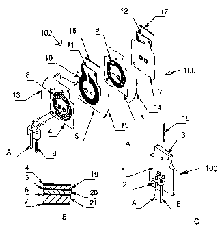
The planar induction sensor 100 shown on Figure
1 comprises multilayer printed board 1 and two-wire
connector 2. This sensor has active zone situated near
edge 3 of the multilayer printed board 1. The multilayer
printed board 1 comprises four active layers 4, 5, 6 and
7, said active layers are separated by glass fibre
laminat separation dielectric layers 19, 20 and 21. All
holes, shown on Figures 1A, 1B and 1C have inner
metallization allowing connection between the wires in
active layers 4,5,6 and 7 associated with the
corresponding hole.
In active layers 4, 5 and 6 there is situated a
current transformer 102 being formed by two series
primary spiral-type coils 8 and 9 and a secondary one-
turn coil 10. Secondary coil 10 of current transformer is
connected to the operating coil 104 being formed by two
wires 11 and 12. Wires 11 and 12 of the operating coil
are situated in the nearest vicinity to sensing edge 3 of
multilayer printed board 1.
Instant directions of alternating currents in
series primary coils 8 and 9 of the current transformer
are shown by arrows 13 and 14, respectively. Alternating
magnetic fields from these currents in the primary coils
generate magnified like-directed currents on both sides
of the secondary one-turn coil of the current transformer
with instant direction is shown by arrow 15. This is the
case when the thickness of the secondary coil material is
at least one skin layer for the material of the secondary
coil at the operating frequency of the induction sensor.
Skin layer thickness is a function of the frequency and
conductance of the material, and is smaller as the
operating the higher operating frequency increases and
CA 02414724 2002-12-18
WH-11 637CA
the conductance of the material decreases. For copper,
the most commonly used material in printed circuit board
technology, at 10 MHz operating frequency the thickness
of skin layer is about 25~m. These calculations should
be taken into consideration in determining the low limit
for the operating frequency of the induction sensor.
Thin separating layers 37 and 38 should be used for
improving efficiency of the current transformer.
Standard separation layers with 0.lmm thickens could be
used for this purpose. The secondary coil of the current
transformer is connected to the operating coil, which is
formed by two wires 11 and 12. The operating coil
contains two wires 11 and 12 with connection to the
secondary coil 10 arranged such that the current flows in
opposite directions as shown in Figure 1 by arrows 16 and
17. Wires 11 and 12 of the operating coil are situated
in the nearest vicinity to sensing edge 3 of the
induction sensor. The distance between wires 11 and 12
is determined by the sum of the thicknesses of separation
layers 20 and 21. Instant direction of testing magnetic
field, formed by the operating coil is shown by arrow 18.
The direction of testing magnetic field lies in the plane
of the printed circuit board 1, being perpendicular to
sensing edge 3 of the induction sensor.
Several factors should be taken into account,
when choosing the separation distance between wires 11
and 12 of operating coil. The higher the magnitude of
the testing magnetic field, the greater is the relative
change in inductance of the sensor when a magnetic or
conductive security element of a tested document passes
the vicinity of sensing edge 3. This relative change in
inductance characterizes the sensitivity of an induction
sensor. The magnitude of the testing magnetic field in
the nearest vicinity of sensing edge 3 increases as
_ g _
CA 02414724 2002-12-18
WH-11 637CA
distance between wires 11 and 12 of the operating coil
decreases. On the other hand, as the distance between
wires 11 and 12 decreases, the active vicinity of sensing
edge 3 decreases and the distance between sensing edge 3
of the induction sensor and the document decreases. This
improves detection of security elements. The sensor that
resolution of separated security elements on a test
document also depends on the distance between wires 11
and 12. The resolution of the sensor increases as the
distance between wires 11 and 12 decreases. Also, if
security elements are closely spaced on a banknote, close
spacing of the wires is required. Therefore, the distance
between wires 11 and 12 depends on t:he particular
application. Particularly, the sensor, shown on the
Figure 1, with l.5mm separation distance between wires 11
and 12 is able to detect magnetic inks on the US
banknotes with a resolution about 2mm if the distance
between sensing edge 3 of the sensor and tested bill is
less then l.5mm. This sensor could be used in banknote
validators without direct contact with the bill and is
able to detect security elements in spite of wobble of
the banknote.
As shown in Figure l, the operating coil of the
induction sensor and the secondary coil of current
transformer are connected with one end of the primary
coil of current transformer. This connection is
necessary to decrease capacitance type sensitivity of
induction sensor. Such sensitivity arises, when large
frequency voltage is present on elements of the sensor,
being nearest to the sensing edge of the sensor. In this
case the banknote and its conductive elements can
influence the capacitance between these elements and the
other group of elements, including the elements of the
induction sensor and elements of associated electronic
- 9 -
CA 02414724 2002-12-18
WH-11 637CA
circuitry. Such type of influence leads to the signals
from associated circuitry, being undistinguishable from
the signals, associated with magnetic security elements
of the banknote. The connection of the operating coil to
the end of the primary coil makes wires A and B of
induction sensor connector 2 nonequivalent. Wire A
should be connected to the common wire of associated
electronic circuit. There is another possibility which
provides more abilities in associated electronic circuit
design where the operating coil does not have any
connection with the primary coil of the current
transformer. The operating coil is connected to the
common wire individually. In the case, when there must
not be any DC coupling between the operating coil and the
primary coil of current transformer an AC connection
through the capacitor should be used.
Figure 2 shows an equivalent electronic circuit
of the induction sensor with the construction, shown on
the Figure 1. The primary coil of the current
transformer consists of two series coils 8 and 9,
connected to the connector 2 of the induction sensor.
Secondary coil 10 of the current transformer is connected
to the operating coil, formed by the wires 11 and 12.
The operating coil has connection with one end of the
currents transformer primary coil and pin A of the
sensors connector 2.
All elements of the planar induction sensor,
including connector 2, are made from nonmagnetic material
to avoid the influence of external magnetic fields on the
sensor. Any ferromagnetic material has dependence of
magnetic permeability on the magnitude of external
magnetic field. Application of such materials in
induction sensor construction leads to dependence of
- 10 -
CA 02414724 2002-12-18
WH-11 637CA
' sensors inductance on the magnitude of the external
magnetic field. Such influence is undesirable, when the
external magnetic field is time-varying. Such fields can
induce a time-varying signal from the associated
circuitry, in many cases being undistinguishable from
that, induced by security elements of documents.
The operating frequency range of the planar
induction sensor, shown in Figure 1,. is from several
megahertz to several tenths of a megahertz. The lower
limit is defined by efficiency of the current transformer
operation. The upper limit is not exactly defined, but
can be estimated as a possible resonant frequency of the
sensor configuration.
Conductive materials, used in planar induction
sensor, should be with the minimum possible specific
resistance. This requirement is useful for the
decreasing of the lower limit of operating frequency
range and improves magnification factor of the induction
sensor inductance. For the same reason printed circuit
board materials with thick metal layers should be used.
As far as such material with low specific resistance as
copper is used in usual printed board technology, it is
easy to meet this requirement. Another materials with
low specific resistance, such as alLrminum or silver,
could be used in construction of induction sensors.
A variant of the planar induction sensor, shown
in Figure 1 is possible by deleting spiral coil 9 and
only using spiral coil 8. The current transformer of
such a construction is not optimal for high frequency
operation, but a sensor with a such current transformer
has a lower frequency low limit.
- 11 -
CA 02414724 2002-12-18
WH-11 637CA
Figure 3 shows another type of the induction
sensor, which differs from that, shown on the Figure 1
only by construction of the operating coil. The sensor
operates in a similar manner with the exception of the
operating coil and the direction of testing magnetic
field. This sensor comprises a multilayer printed
circuit board 22 with two-wire connector 23. The
multilayer printed circuit board has three active layers
25, 26 and 27, mounted on the dielectric substrate 39 and
being separated by dielectric layers 37 and 38. The
current transformer comprises two series spiral-type
primary coils 28 and 22 and one- turn secondary coil 30,
being situated in active layers 25, 26 and 27,
correspondingly. Instant directions of currents in the
coils of the current transformer are shown by arrows 32,
34 and 33. The main distinction of the sensor, shown in
Figure 3 from the sensor of Figure L, is the operation
coil, being formed by one wire 31. The wire is situated
near the sensing edge 24 of the induction sensor.
Instantaneous current direction in this wire is shown by
the arrow 35. This current induces a testing magnetic
field which direction in the nearest vicinity of sensing
edge 24 of the sensor, is shown by the arrow 36. This
testing magnetic field direction is perpendicular to the
sensors printed circuit board 22 plane and lies in the
plane of the tested document. Such a sensor has
sensitivity dependence on the distance from sensing edge
to the tested document and as such, is less precise
relative to the sensor of Figure 1.
Figure 4 shows equivalent electronic circuit of
the induction sensor of the construction, shown in Figure
3. All unit numbers on Figure 4 correspond to that, shown
on the Figure 3. The primary coil of the current
transformer consists of two series coils 28 and 29,
- 12 -
CA 02414724 2002-12-18
WH-11 637CA
" connected to connector 23 of the induction sensor.
Secondary coil 30 of the current transformer is connected
to the operating coil, formed by wire 31. The operating
coil is connected with one end of the current is
transformer primary coil and pin A of sensors connector
23.
Figure 5 shows another type of induction sensor
with more complicated structure of the current
transformer. The sensor comprises a multilayer printed
board 40 and two-wire connector 41. All holes, shown on
Figure 5, have inner metallization f=or connection between
the wires in active layers 43, 44, 45, 46, 47 and 48
associated with the corresponding hole. This sensor has
an active zone situated near the edge 42 of the
multilayer printed board 40. This Censor is similar to
the sensor of Figure 1 and differs from it due to the
improved construction of the current transformer. The
current transformer in this case contains three primary
coils 49, 50 and 51 in different layers 44, 46 and 48.
All this primary coils are connected in series. Arrows
54, 55 and 56 shows the instant directions of currents in
these primary coils. Secondary coil of the current
transformer is situated in layers 45 and 47 of printed
circuit board and contains two turns 52 and 53, being
connected in series. Operating coil of this sensor is
formed near the sensing edge 42 of t:he printed circuit
board 40 by the wires 60 and 61 in the layers 43 and 48.
These wires are connected in series to the current
transformer. Instant currents in the wires of operating
coil have opposite directions, shown by the arrows 61 and
62. The instant direction of testing magnetic field,
induced by the operating coil, is shown by the arrow 63
and lies in the plain of the printed circuit board 40 and
is perpendicular to the sensing edge 42. All active
- 13 -
CA 02414724 2002-12-18
WH-11 637cA
layers 43, 44, 45 46, 47 and 48 are separated by glass
fibre laminat separation dielectric layers 64, 65, 66, 67
and 68. Thickness of the layers 64, 65, 66 and 67 should
be as thin as practical for the effective operation of
current transformer. The distance between wires 59 and
60 is determined by the sum of the thicknesses of
separation layers 64, 65, 66, 67 and 68.
Figure 6 shows an equivalent electronic circuit
of the induction sensor with the construction, shown on
the Figure 5. The primary coil of the current
transformer has three series coils X69, 50 and 51,
connected to the connector 41 of the induction sensor.
Secondary coil of the current transformer consists from
two series one-turn coils 52 and 53 being connected to
the operating coil. The operating coil contains two
series wires 61 and 62.
Figure 7 shows another type of induction sensor
with the current transformer, similar to that, shown in
Figure 5. This sensor comprises multilayer printed board
69 and two-wire connector 70. All holes, shown on Figure
7, have inner metallization for connection between the
wires in active layers 72, 73, 74, 75, 76 and 77 are
associated with the corresponding he>le. This sensor has
an active zone situated near the edge 71 of the
multilayer printed board 69. The sensor is similar to
that, shown in Figure 3 while having an improved
construction of the current transformer and operating
coil. The current transformer contains three primary
coils 78, 79 and 80 in different layers 73, 75, and 77.
All of the primary coils are connected in series. Arrows
87, 88 and 89 shows the instant directions of currents in
the primary coils. Secondary coil of the current
transformer is situated in layers 74 and 76 of printed
- 14 -
CA 02414724 2002-12-18
WH-11 637CA
circuit board and contains two turns 81 and 82, connected
in series. The operating coil of this sensor is formed
near the sensing edge 71 of the printed circuit board 69
by the wires 83, 84, 85 and 86 in the layers 73, 74, 75
and 76. These wires are connected in parallel to the
current transformer. Instant currents in the wires of the
operating coil have the directions shown by the arrows
92, 93, 94 and 95. The instant direction of testing
magnetic field, induced by the operating coil, is shown
by the arrow 96 and is perpendicular to the plane of the
printed circuit board 69 and parallel to the sensing edge
71. All active layers 72, 73, 74, 75, 76 and 77 are
separated by glass fibre separation dielectric layers 97,
98, 99, 100 and 101. Thickness of the layers 97, 98, 99
and 100 should be as thin as practical for the effective
operation of current transformer. Thickness of the layer
101 is not important.
Figure 8 shows an equivalent electronic circuit
of the induction sensor with the construction, as shown
in Figure 7. The primary coil of the current transformer
has three series coils 78, 79 and 80, connected to the
connector 70 of the induction sensor. The secondary coil
of the current transformer has at least series one-turn
coils 81 and 82 connected to the operating coil. The
operating coil contains four wires 83, 84, 85 and 86
connected in parallel.
The main task of the induction sensors design
is to concentrate the magnetic field energy near the
sensing edge of the induction sensor'. Any magnetic
fields in the other parts of the sensor should be
minimized. Application of this demand to the sensors,
shown on Figures 1, 3, 5 and 6, means the minimization of
- 15 -
CA 02414724 2002-12-18
WH-11 637CA
the magnetic field in the vicinity of current
transformer. It is seen from the Figures 1, 3, 5 and 6,
that currents in the primary and secondary coils of the
current transformer have opposite directions. This fact
leads to the compensation of magnetic fields, associated
with these currents, in the vicinity of the current
transformer. The efficiency of the current transformer
depends on the thickness of the separation layers, wires
material properties and its thickness and the chosen
operation frequency. There are also several geometry
aspects, influencing the quality of the current
transformer. All of the secondary coil should be covered
by primary coils. Current in any part of the secondary
coil without exciting turns of primary coil in the
nearest vicinity will induce uncompensated magnetic field
in its vicinity. The currency transformer can be further
improved by the correct geometry of primary coil of
current transformer.
Figure 9 shows three typed> of primary coils of
the current transformer. Spiral-type coil 102 has
constant width of turns and constant distance between
turns. For complete compensation of magnetic field
induced by the current in this type of coil, a uniform
distribution of current density in the secondary coil of
the current transformer is required. Such current
distribution is not possible as it implies different
magnitude of voltages on the secondary coil ends, caused
by the currents on the inner and outer edges of secondary
coil. For this reason, compensation. for coil 102 will
only be achieved in the region of the middle turns of the
coil. Application of such a coil is justified in the
case of a current transformer configuration, when the
lengths of inner and outer turns differ slightly.
Configuration of spiral-type coils 103 and 104, shown in
- 16 -
CA 02414724 2002-12-18
WH-11 637CA
the Figure 9, allow complete compensation in all
vicinities of the current transformer. Coil 103 has
constant width of the turns with variable distance
between turns, being greater as the length of the turn
increases. Coil 104 has constant separation distance
between turns with variable width of the turns, being the
greater, as the length of turns increases. Variable
parameters for coils 103 and 104 are so, that excited
current distribution in secondary coil of current
transformer is optimal for this coil-.
There are known electronic circuits for
processing signals from induction sensors. The
electronic circuits convert changes in inductance of the
induction sensor in available signals, such as
proportional to changes in voltage or alternating voltage
with frequency, depending on this changes. Such
circuitry can be placed on the printed circuit board of
induction sensor, forming a fully integrated magnetic
channel. It is also possible to place of the associated
electronic circuit is placed on printed circuit board.
Figure 10 shows a one-side application of
planar induction sensor in a bill validator. In this
application induction sensor 105 is disposed on one side
of a plane of movement of the bill. The plane of the
induction sensor printed circuit board is perpendicular
to the plane of the tested bill 108. Induction sensor
sensing edge is situated in the nearest vicinity of the
path that the bill 108 will make along. The direction of
movement of bill 108 is shown by the arrow 109.
Electronic circuit 106 forms the signal as a function of
changes in inductance of induction sensor 105. Analyzing
of this signal is completed by microcontroller 107. The
one side application as shown in Figure 10, analyzes only
- 17 -
CA 02414724 2002-12-18
,WH-11 637CA
one track of the bill. If it is necessary, several
induction sensors can be placed near the bill path to
analyze different tracks of the bill.. In the case of the
planar induction sensors application, multiple sensors
can be formed in one printed circuit board. All
associated electronic circuitries can also be placed on
the printed board, forming complete mufti-channel
magnetic sensors assembly.
The main disadvantage of the one-side
application, shown in Figure 10, is the signals magnitude
depends upon the distance from the bill to the induction
sensor. If mechanical arrangements for keeping the bill
at a constant distance from the sensor are not used, only
presence or absence of a security element are detected
and such features of security elements as magnetic and
conductive properties can only estimated.
Figure 11 shows the arrangement of a planar
induction sensor, which takes into account dependence of
the signals on the distance from the sensor to the bill
even in the case of document wobble in the validator
channel. This arrangement comprises. two planar induction
sensors 110 and 111 with individual associated electronic
circuit 112 and 113, placed on opposite sides of the
validator channel directly opposite one another. Signals
from both sensors are analyzed by microcontroller 114.
Bills movement direction is shown by the arrow 115. If
the distance between sensors 110 and 111 and individual
sensitivities of each of the sensors is known, the
instantaneous ratio between magnitudes of the signals
from each sensor characterizes the position of the tested
security element between the sensors at the same instant.
Information about position along with known function
dependence of the signal on the distance from the sensor
- 18 -
CA 02414724 2002-12-18
WH-11 637CA
to the tested security element allows calculation of the
real amplitude of the signal despite any wobble of the
bill in the channel of the validator. This complex
procedure with many terms is simplified due to the high
extent of reproducibility of the printed board technology
of main parameters of planar induction sensors, such as
sensitivity and function of dependence of the sensitivity
on the distance from sensor to tested security element.
Although various preferred embodiments of the
present invention have been described herein in detail,
it will be appreciated by those skilled in the art, that
variations may be made thereto without departing from the
spirit of the invention or the scope of the appended
claims.
- 19 -