Note : Les descriptions sont présentées dans la langue officielle dans laquelle elles ont été soumises.
CA 02415564 2003-O1-03
The present invention relates to an optical pulse pattern
generator, and more particularly to an optical pulse pattern
generator capable of generating a pulse train for optical
labeling and an optical random pattern pulse train for device
evaluation in an optical communication field.
As optical communication systems increase their capacity,
high-speed transmission systems with a bit rate of 40 Gb/s per
channel is nearing practical use. In addition, major carriers
Zo and vendors in the U . S . , Europe and Japan promote research and
development of next generation ultrahigh-speed transmission
systems with a bit rate of 100 Gb/s or more per channel.
Furthermore, intensive research and development of optical
network systems that carry out all-optical routing of optical
signals have been conducted. It is essential for a high-speed
transmission system to evaluate the optical system and devices
using high-speed optical random pattern pulse train, and for
an optical network system to generate a high-speed label pulse
train for optical packets.
2o Fig. 1 shows a conventional optical pulse pattern generator
used for the foregoing purposes . In the optical pulse pattern
generator shown in Fig. 1, an optical pulse train with a period
T from an optical pulse source 1 is supplied to an input 2 , and
is split by an optical sputter 3. Then, individual optical
pulses pass through optical waveguides 4-1 to 4-N, where N is
an integer greater than one, and are led to optical switches
5-1 to 5-N. The optical pulses pass through only optical
switches in a bar state among the optical switches 5-1 to 5-N
CA 02415564 2003-O1-03
to be led to the delay lines 6-1 to 6-N, and are coupled by optical
combiners 7 to be output from an output 8 . In this case, if length
differences of the delay lines 6-1 to 6-N increase step by step
by an amount of cT/(nN) in this order, an optical random pattern
pulse train with a period T and a sequence length N is generated,
where c is the light speed in the vacuum, and n is the group
refractive index of the delay lines . The optical random pattern
pulse train corresponds to the bar state ( 1 ) or a cross state
(0) in each of optical switches.
so Therefore to generate the optical random pattern pulse
train with the period T and sequence length N, the foregoing
conventional method must include N optical switches and N delay
lines, thereby complicating the configuration because of an
increase in the number of components and the size thereof . In
addition, it requires 1xN optical splitter 3 and Nx1 optical
combiner 7, thereby increasing the loss.
For example, "Large-capacity WDM packet switching" K.
Habara et al. , Springer Photonic Networks (G. Prati Ed. ) , 1997
discloses in pp.285 to 299 a method of repeatedly launching
20 optical pulses onto an optical device composed of an optical
combiner and splitter, a delay line array and an optical switch
array. However, it requires the same number of the delay lines
and switches as the sequence length needed. Accordingly, its
size increases and its configuration becomes complicated at a
typical sequence length. In addition, since the number of the
input ports of the combiner and that of the output ports of the
splitter must also be equal to the sequence length, its loss
increases with an increase in the sequence length.
- 2 -
CA 02415564 2003-O1-03
Furthermore, R.J.S.Pedersen, B.F.Jorgensen, M.Nissov and
He Yongqi, "lOGbit/s repeaterless transmission over 250km
standard fibre" ELECTRONICS LETTERS, 7th November 1996, 'Vol. 32,
No. 23 discloses in pp.2155 to 2156, a method of modulating CW
light by driving an optical modulator by an electric pulse
pattern. However, it is difficult for it to generate a pulse
pattern beyond 40 Gb/s because of the limit of the operation
speed of the pulse pattern generator in an electrical region.
Furthermore , U . S . patent No . 5 , 208 , 705 discloses a method
of utilizing a feedback shift register composed of an optical
exclusive OR circuit based on nonlinear optical effect in
combination with an optical fiber fixed delay lines. However,
since it must use two types of optical pulses (clock pulse and
control pulse ) , its configuration becomes large and complicated.
In addition, using the nonlinear optical effect imposes some
conditions on the operable optical pulse intensity, and makes
its operation unstable. Furthermore, using optical fiber fixed
delay lines makes it difficult to adjust the delay line length
accurately, and to vary the pulse pattern, pulse period or bit
2o rate .
As described above, no effective high-speed optical pulse
train generating means are reported up to now. Consequently,
implementing a small, stable all-optical pulse pattern
generator that is not governed by the speed of electric
components has been expected.
The present invention is implemented to solve the foregoing
problems. It is therefore an object of the present invention
- 3 -
CA 02415564 2003-O1-03
to provide an optical pulse pattern generator with a simple
configuration and low loss.
According to a first aspect of the present invention, there
is provided an optical pulse pattern generator comprising: an
optical pulse source for generating an optical pulse; an optical
combiner and splitter having two inputs and two outputs, a first
input of the two. inputs of which is connected to the optical
pulse source; a variable optical delay line circuit having two
inputs and two outputs and including a plurality of
io cascade-connected characteristic-variable asymmetrical
Mach-Zehnder interferometers each of which has two inputs and
two outputs, a first output of one of the cascade-connected
characteristic-variable asymmetrical Mach-Zehnder
interferometers being connected to a first input of another of
the cascade-connected characteristic-variable asymmetrical
Mach-Zehnder interferometers to form a cascade connection
therebetween, and a first input of the variable optical delay
line circuit being connected to a first output of the optical
combiner and splitter; and one or more optical exclusive OR
2o circuits, and inputs of the optical exclusive OR circuits being
connected to second outputs of the cascade-connected
characteristic-variable asymmetrical Mach-Zehnder
interferometers respectively, wherein a first output of the
optical exclusive OR circuits is connected to a second input
of the optical combiner and splitter.
Here, the optical exclusive OR circuits may be cascaded.
Each of the optical exclusive OR circuis may have two inputs
and two outputs, and the number of the optical exclusive OR
- 4 -
CA 02415564 2003-O1-03
circuits may be less than the number of the cascade-connected
characteristic-variable asymmetrical Mach-Zehnder
interferometers by one.
Each of the cascade-connected characteristic-variable
asymmetrical Mach-Zehnder interferometers may include at least
one characteristic-variable asymmetrical Mach-Zehnder
interferometer comprising: a first directional coupler with
variable coupling ratio having two inputs and two outputs; and
a second directional coupler with variable coupling ratio having
to two inputs and two outputs connected to the first directional
coupler with variable coupling ratio through two optical
waveguides with different lengths.
A first output of one of the characteristic-variable
asymmetrical Mach-Zehnder interferometers may be connected to
a first input of another of the characteristic-variable
asymmetrical Mach-Zehnder interferometers to form a cascade
connection of the two as each of the cascade-connected
characteristic-variable asymmetrical Mach-Zehnder
interferometers.
2o One of the first and second directional couplers with
variable coupling ratio may be used in common by two of the
characteristic-variable asymmetrical Mach-Zehnder
interferometers.
The optical pulse pattern generator may further comprise
at least one optical amplifier at a position on a light path.
The optical combiner and sputter may consist of a
symmetrical Mach-Zehnder interferometer.
Each of the optical exclusive OR circuits may consist of
- 5 -
CA 02415564 2003-O1-03
a symmetrical Mach-Zehnder interferometer.
The optical pulse pattern generator may further comprise
an optical gating device connected to an output of one of the
variable optical delay line circuit, the optical combiner and
splitter and the optical exclusive OR circuits.
According to a second aspect of the present invention, there
is provided an optical pulse pattern generator comprising: an
optical pulse source for generating an optical pulse; an optical
combiner and splitter connected to an output of the optical pulse
Zo source; a variable optical delay line circuit connected to the
optical combiner and splitter; and one or more optical exclusive
OR circuits connected to the variable optical delay line circuit
at intermediate stages and a final stage of the variable optical
delay line circuit , wherein one output of the optical exclusive
OR circuits is connected to the optical combiner and splitter.
According to a third aspect of the present invention, there
is provided an optical pulse pattern generating method of
generating an optical random pattern pulse train from an optical
pulse, the optical pulse pattern generating method comprising
2o the steps of : launching an optical pulse produced by an optical
pulse source to a variable optical delay line circuit via an
optical combiner and splitter, the variable optical delay line
circuit including a plurality of cascade-connected
characteristic-variable asymmetrical Mach-Zehnder
interferometers; supplying an optical pulse output from each
of the cascade-connected characteristic-variable asymmetrical
Mach-Zehnder interferometers to the optical combiner and
splitter through one or more optical exclusive OR circuits; and
- 6 -
CA 02415564 2003-O1-03
producing a random pulse train from one of the variable optical
delay line circuit, the optical combiner and splitter and the
optical exclusive OR circuits by using the optical pulse supplied
to the optical combiner and splitter.
According to the present invention, the output of the
optical pulse source is connected to the variable optical delay
line circuit via the optical combiner and splitter. The
variable optical delay line circuit feeds back from its
intermediate or final stage the optical pulse to the optical
Zo combiner and splitter via the optical exclusive OR circuits.
The configuration can implement a linear feedback shift register
in the optical region. Adjusting the length of the variable
optical delay line circuit makes it possible to generate optical
random pattern pulse trains with various periods and patterns ,
thereby being able to realize the optical pulse pattern
generator.
Furthermore, the optical pulse pattern generator in
accordance with the present invention, by applying the variable
linear feedback shift register configuration in the optical
2o region, can generate the optical pulse patterns with various
periods and patterns with a small size, low loss, integrated
configuration without using a high-speed intensity modulator.
The above and other objects, effects, features and
advantages of the present invention will become more apparent
from the following description of embodiments thereof taken in
conjunction with the accompanying drawings.
Fig. 1 is a block diagram showing a configuration of a
CA 02415564 2003-O1-03
conventional optical pulse gattern generator;
Fig. 2 is a block diagram showing a configuration of a first
embodiment of the optical pulse pattern generator in accordance
with the present invention;
Fig . 3 is a block diagram showing a configuration of a 3dB
directional coupler;
Figs. 4A to 4C are views showing a configuration of a
directional coupler with variable coupling ratio;
Figs . 5A to 5E are diagrams illustrating the operation of
to the embodiment of the optical pulse pattern generator in
accordance with the present invention;
Figs . 6A to 6E are diagrams illustrating the operation of
the embodiment of the optical pulse pattern generator in
accordance with the present invention;
Fig. 7 is a block diagram showing a configuration of a second
embodiment of the optical pulse pattern generator in accordance
with the present invention;
Fig. 8 is a block diagram showing a configuration of a third
embodiment of the optical pulse pattern generator in accordance
2o with the present invention;
Fig. 9 is a block diagram showing a configuration of a
variation of the embodiments of the optical pulse pattern
generator in accordance with the present invention; and
Fig. 10 is a block diagram showing a configuration of a
variation of the embodiments of the optical pulse pattern
generator in accordance with the present invention.
The invention will now be described with reference to the
CA 02415564 2003-O1-03
accompanying drawings.
FIRST EMBODIMENT
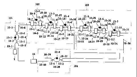
Fig. 2 shows a first embodiment in accordance with the
present invention. As shown in this figure, the present
embodiment of the optical pulse pattern generator comprises an
optical pulse source 9, optical waveguides 10-1 to 10-40,
directional couplers 11-1 to 11-12 with variable coupling ratio,
3-dB directional couplers 12-1 to 12-4, waveguide refractive
io index control sections 13-1 to 13-8, and an optical amplifier
14.
In the present embodiment , the output of the optical pulse
source 9 is connected to a cascade connection of a first
symmetrical Mach-Zehnder interferometer used as an optical
combiner and splitter 101, and first and second cascade-
connected characteristic-variable asymmetrical Mach-Zehnder
interferometers 102 and 103. The two cascade-connected
characteristic-variable asymmetrical Mach-Zehnder
interferometers 102 and 103 have their final stages connected
2o to the first symmetrical Mach-Zehnder interferometer 101 via
a second symmetrical Mach-Zehnder interferometer used as an
optical exclusive OR circuit 104 and via the optical amplifier
14 , thereby constituting a feedback loop . The number of stages
of each of the cascade-connected characteristic-variable
asymmetrical Mach-Zehnder interferometers 102 and 103 , that is ,
the number of the characteristic-variable asymmetrical
Mach-Zehnder interferometers, is three.
Cascading the two two-input/two-output cascade-connected
_ g _
CA 02415564 2003-O1-03
characteristic-variable asymmetrical Mach-Zehnder
interferometers 102 and 103 can constitute a two-input/two-
output variable optical delay line circuit. Specifically,
connecting a first output port of the previous cascade-connected
characteristic-variable asymmetrical Mach-Zehnder
interferometer 102 with a first input port of the subsequent
cascade-connected characteristic-variable asymmetrical
Mach-Zehnder interferometer 103 in series constitutes the
two-input/two-output variable optical delay line circuit.
1o The optical pulse source 9 is connected to a first input
port of the optical combiner and splatter 101 via the optical
waveguide 10-1. A first output port of the optical combiner and
splatter 101 is connected to a first input port of the variable
optical delay line circuit (cascade-connected
characteristic-variable asymmetrical Mach-Zehnder
interferometer 102) via the optical waveguide 10-6. A second
output port of the cascade-connected characteristic-variable
asymmetrical Mach-Zehnder interferometer 102 and a first output
port of the cascade-connected characteristic-variable
2o asymmetrical Mach-Zehnder interferometer 103 are both connected
to input ports of the optical exclusive OR circuit 104 via the
optical waveguides 10-21 and 10-36. A first output port of the
optical exclusive OR circuit 104 is connected to a second input
port of the optical combaner and splatter 101 via the optical
waveguide 10-40, optical amplifier 14 and optical waveguide 10-2 .
In Fig . 2 , the optical waveguide is an open output port ( output ) .
Incidentally, a second output port of the cascade-connected
characteristic-variable asymmetrical Mach-Zehnder
- to -
CA 02415564 2003-O1-03
interferometer 103 can be connected to the input port of the
optical exclusive OR circuit 104 via the optical waveguide 10-35
to use the optical waveguide 10-36 as an open output port
(output).
The cascade-connected characteristic-variable
asymmetrical Mach-Zehnder interferometers 102 and 103 each
include three characteristic-variable asymmetrical Mach-
Zehnder interferometers. Each characteristic-variable
asymmetrical Mach-Zehnder interferometer includes a pair of
so two-input/two-output directional couplers with variable
coupling ratio connected in cascade. More specifically, the
input side two-input/two-output directional coupler with
variable coupling ratio ( 11-1, for example) has its two output
ports connected to the two input ports of the output side
two-input/two-output directional coupler with variable
coupling ratio ( 11-2 , for example ) via the two optical waveguides
(10-8 and 10-9, for example) with different length. Then, the
previous characteristic-variable asymmetrical Mach-Zehnder
interferometer has its first output port connected in series
2o to the first input port of the subsequent characteristic-
variable asymmetrical Mach-Zehnder interferometer.
The two cascade-connected characteristic-variable
asymmetrical Mach-Zehnder interferometers 102 and 103 can be
arranged into a single characteristic-variable asymmetrical
Mach-Zehnder interferometer.
The 3-dB directional couplers 12-1 to 12-4 are each composed
of two optical waveguides 15-1 and 15-2 of several micrometer
square that are placed side by side in close proximity in the
- 11 -
CA 02415564 2003-O1-03
order of a few micrometers as shown in Fig . 3 , such that a 50 a
power coupling is achieved by adjusting the length of the
proximate section(coupling length). Inthe proximate type3-dB
directional coupler, the phase of a transmitted wave is shifted
by a~/2 from that of a reflected wave. The 3-dB directional
coupler can also be formed using an MMI (multimode interference)
coupler configuration.
The directional couplers with variable coupling ratio 11-1
to 11-12 can be composed of a symmetrical Mach-Zehnder
to interferometer as shown in Fig. 4A. The directional couplers
with variable coupling ratio 11-1 to 11-12 each include optical
waveguides 16-1 to 16-6, 3-dB directional couplers 17-1 and 17-2,
and a waveguide refractive index control sections 18.
Figs . 4B and 4C are cross-sectional views taken along lines
b-b and c-c of Fig. 4A, respectively, in which the directional
coupler with variable coupling ratio is composed of silica glass
waveguides.
As shown in Fig . 4B , the directional couplers with variable
coupling ratio 11-1 to 11-12 each include at the b-b cross section
2o a silicon substrate 19-1, an under cladding 20-1 and an over
cladding 22-1 stacked in this order. In the over cladding 22-1,
cores 21-1 and 21-2 are formed on the side facing the under
cladding 20-1 . In addition, as shown in Fig. 4C, the directional
couplers with variable coupling ratio 11-1 to 11-12 each include
at the c-c cross section, a silicon substrate 19-2, an under
cladding 20-2 and an over cladding 22-2 stacked in this order.
In the over cladding 22-2, cores 21-3 and 21-4 are formed on
the side facing the under cladding 20-2. On the over cladding
- 12 -
CA 02415564 2003-O1-03
22-2, a thin film heater 23 is provided for controlling the
refractive index of the waveguide of the core 21-3 by heating.
Varying the phase of the waveguide between 0 and 2~t using
the control section 18 enables the switching characteristics
of the symmetrical Mach-Zehnder interferometer to set the power
coupling ratio between the input and output ports at any desired
value between 0 and 100. If the power coupling ratio of the
3-dB directional coupler deviates from 50~ because of a
fabrication error and the like, it is difficult for the
to configuration of Fig. 4A to achieve any desired coupling ratio.
In this case, replacing the single symmetrical Mach-Zehnder
interferometer with a multi-stage configuration makes it
possible to achieve any desired coupling ratio. Utilizing the
symmetrical Mach-Zehnder interferometer configuration of Fig.
4A can implement an optical combiner and splitter. It is obvious
that the optical combiner and splitter can also be constituted
using a directional coupler configuration.
Returning to Fig . 2 , the waveguide refractive index control
sections 13-1 to 13-8 and 18 can utilize a thin film heater
zo (thermooptic effect) or the like, when the waveguide to be
controlled is composed of a glass waveguide or polymer waveguide .
On the other hand, when the wave guide to be controlled is composed
of a dielectric waveguide or semiconductor waveguide, they can
utilize an electrode (electric optical effect) or the like.
As the optical amplifier 14 , it is possible to use a rare
earth doped optical fiber amplifier such as an erbium-doped
optical fiber amplifier (EDFA), a rare earth doped optical
waveguide, or a semiconductor laser optical amplifier (SOA).
- 13 -
CA 02415564 2003-O1-03
As the optical pulse source 9, it is possible to use a
semiconductor or optical fiber mode locked laser, a
semiconductor gain switched light source, or a pulsed light
generated by intensity modulation of a CW light source with a
polymer or a dielectric such as LN, or a semiconductor EA
modulator.
Next, by referring to Figs. 5A to 5E, the operation of the
optical pulse pattern generator as shown in Fig. 2 will be
described in detail. Fig. 5A shows the output pulses (period
to dt ) of the optical pulse source 9 . As the directional couplers
with variable coupling ratio 11-1 to 11-5 and 11-7 to 11-11,
a switching function whose coupling ratio is 0~ or 100 is used.
In addition, as the directional couplers with variable coupling
ratio 11-6 and 11-12, a coupling ratio. variable function is used.
The length differences between upper and lower arms of each of
the asymmetrical Mach-Zehnder interferometers shown in Fig. 2
are assumed to be ~Lj ( j = 1 to 6 ) . In this case, it is possible
for the path between the optical waveguide 10-6 and optical
waveguides 10-20 and 10-21 and for the path between the optical
2o waveguide 10-20 and optical waveguides 10-35 and 10-36 to have
variable delay differences between arms ranging from zero to
(~L1 + /~L2 + ~L3 ) and from zero to (0L4 + OL5 + OL6 ) with a minimum
unit ~Lj, respectively. In addition, intensities of the pulses
arriving at the optical waveguides 10-21 and 10-36 can be made
equal.
Incidentally, as for waveguide lengths except for those in
the variable delay line sections, they are not mentioned in the
description because they have no substantial relation to the
- 14 -
CA 02415564 2003-O1-03
operation of the present embodiment of the optical pulse pattern
generator. However, adjustment of the waveguide lengths for
enabling the operation shown in Figs. 5A to 5E is carried out
as needed (for example, the lengths at the portions of the optical
waveguides 10-22 and 10-36 are made equal), which is easily
achieved by using optical waveguide technology.
The symmetrical Mach-Zehnder interferometer 104, in which
the phase difference between the optical waveguides 10-37 and
10-38 is set at ~c/2 by adjusting the optical path length in a
2o wavelength size order in the design and fabrication process,
or by driving the waveguide refractive index control section
23-8, can operate as an optical exclusive OR circuit. The
relationships among the presence and absence of the input (x1 )
at the optical waveguide 10 - 21, and that of the input ( x2 ) at
the optical waveguide 10-36 and the output (y) at the optical
waveguide 10-40 are summarized in Table 1.
Table 1
xI x2 Y
0 0 0
o ~ I
1 0 I
I I 0
- 25 -
CA 02415564 2003-O1-03
It is assumed here that the phase difference between the
input optical pulses x1 and x2 supplied via the optical
waveguides 10-21 and 10-36 are set at an integer multiple of
2~c within a coherence length of the light source by controlling
the optical path length in the wavelength size or smaller order
in the design and fabrication process, or by operating at least
one of the waveguide refractive index control sections 13-2 to
13-7 to adjust the phase of the lightwaves.
Table 1 shows that the output y is the exclusive OR of the
so inputs x1 and x2 satisfying the following expression ( 1 ) . In
expression ( 1 ) , an overline indicates "not " of the digital signal .
Such an optical exclusive OR function can be achieved by using
the nonlinear optical effect of a semiconductor laser optical
amplifier or the like.
y = xlx2 + xlx2 ~ x2 +O x2 ( 1 )
The configuration shown in Fig. 2 having the exclusive OR
function and feedback function constitutes a linear feedback
2o shift register in an optical region. The optical amplifier 14
can compensate for the drops in the pulse intensity levels due
to the waveguide loss and splitting.
Figs . 5B, 5C, 5D and 5E illustrate behaviors of pulses at
the optical waveguides 10-21, 10-36, 10-40 and 10-35 (output),
respectively, when a delay La is given between the optical
waveguide 10 - 6 and the optical waveguides 10 - 2 0 and 10 - 21, and
a delay Lb is given between the optical waveguide 10-20 and the
optical waveguides 10-35 and 10-36 . Here, La = {cT/ ( 15n) - l~
- 16 -
CA 02415564 2003-O1-03
and Lb = { 3cT/ ( 15n) - 1} , where 1 is the clockwise distance from
the optical waveguides 10-21 and 10-36 to the optical waveguide
10-6. For example, the above delays can be achieved as follows.
~L1 - ~L4 - cT/(15n) -3L - 1,
~L2 - ~L3 - OL5 = OL6 - cT/(15n),
La = ~L1 + 3L,
Lb = ~L4 + 4L5 + OL6 + 3L
io Incidentally, L represents lower arm length in each
characteristic-variable asymmetrical Mach-Zehnder inferometer.
We assumed that the lov~ter arm lengths are equal in all the six
interferometers. In addition, the effect of delay caused by
unsubstantial waveguide lengths such as the distance from the
optical waveguides 10-21 and 10-36 to the optical waveguide 10-40
is not shown in Figs. 5A-5E: Figs. 5A-5E show that a pulse
pattern of M sequences (Maximum Length Shift Register Sequences)
with period T and sequence length 15 , that is , a typical random
pulse train, can be implemented.
2o Figs . 6A-6E illustrate the behaviors of the pulses when the
delays Lb f = 3cT/ ( 15n) - 1} and La ~= cT/ ( 15n) - 1} are assigned
to the path between the optical waveguide 10-6 and the optical
waveguides 10-20 and 10-21 and to the path between the optical
waveguide 10-20 and the optical waveguides 10-35 and 10-36,
respectively. Figs. 6A-6E show the behaviors at the same
positions as those of Figs. 5A-5E.
Figs . 5A-5E and Figs . 6A-6E show that the variable optical
random pattern pulse train with a sequence length 15 (= 24 -
- m -
CA 02415564 2003-O1-03
1 ) can be obtained by using only four of the six delay devices
( the conventional example uses 15 delay devices ) . The ratio of
the number of the delay devices of the present embodiment to
that of the conventional example decreases with an increase of
the sequence length. This means that the advantage of the
present configuration over the conventional example becomes
conspicuous as the sequence length of the optical random pattern
pulse train increases.
When the following expression ( 2 ) is satisfied, the pulses
io fed back from the optical waveguide 10-2 to the optical waveguide
10-6 do not collide with the pulses in the next period from the
optical pulse source 9.
fit= f »T (2)
where f is the repetition frequency of the optical pulse source
9.
The optical pulse source satisfying the above condition can
be implemented by a mode-locked fiber laser or the like. For
2o example, an optical pulse source with a repetition frequency
of 10 MHz and a pulse width of a few picoseconds has been
implemented. When generating a pulse pattern with a pulse
period of lops (repetition frequency 100 GHz) and a sequence
length of 25 (with a period of 150 ps and a repetition frequency
of 6.7 GHz) by using the foregoing light source and silica-
based waveguides (with group refractive index of about 1.5),
the left-hand side of the inequality sign of the foregoing
- is -
CA 02415564 2003-O1-03
expression ( 2 ) becomes t1t = 1/f = 105 ps, and the right-hand side
becomes T = 150 ps . Thus, it is very easy to satisfy the condition
of the expression (2).
Even if the condition of expression ( 2 ) is not satisfied,
the operation as the optical pulse pattern generator is the same
when the following conditions are satisfied: (1) at = KT, where
K is a natural number; and ( 2 ) the phase of the optical pulses
fed from the optical pulse source 9 differs from the phase of
the feedback optical pulses by an integer multiple of 2~c at the
to optical waveguide 10-6, because only the signal intensity of
the "1" as digital signal increases in this case.
SECOND EMBODIMENT
Fig. 7 shows a second embodiment in accordance with the
present invention. In this figure, the optical pulse source 24
is connected to a cascade connection of a first symmetrical
Mach-Zehnder interferometer used as an optical combiner and
splitter 201, and first and second cascade-connected
characteristic-variable asymmetrical Mach-Zehnder
2o interferometers 202 and 203. The two cascade-connected
characteristic-variable asymmetrical Mach-Zehnder
interferometers 202 and 203 have their final stages connected
to the first symmetrical Mach-Zehnder interferometer 201 via
a second symmetrical Mach-Zehnder interferometer used as an
optical exclusive OR circuit 204 and an optical amplifier 29,
thereby constituting a feedback loop. The number of stages in
each of the cascade-connected characteristic-variable
asymmetrical Mach-Zehnder interferometers 202 and 203 is three.
- 19 -
CA 02415564 2003-O1-03
As shown in Fig. 7, the present embodiment of the optical
pulse pattern generator comprises the optical pulse source 24 ,
optical waveguides 25-1 to 25-28, directional couplers with
variable coupling ratio 26-1 to 26-8, 3-dB directional couplers
27-1 to 27-4, waveguide refractive index control sections 28-1
to 28-8, and optical amplifier 29.
The cascade-connected characteristic-variable
asymmetrical Mach-Zehnder interferometers 202 and 203 in Fig.
7 differs from the cascade-connected characteristic-variable
Zo asymmetrical Mach- Zehnder interferometers 102 and 103 in Fig .
2 in that the ports of the directional couplers with variable
coupling ratio are connected via a pair of paths rather than
via a single path.
For example, the cascade-connected characteristic-
variable asymmetrical Mach-Zehnder interferometer 202 includes
the four two-input/two-output directional couplers with
variable coupling ratio 26-1 to 26-4. Then, the input side
two-input/two-output directional coupler with variable
coupling ratio (26-1, for example) has its two output ports
as connected to the two input ports of the output side two-
input/two-output directional coupler with variable coupling
ratio ( 26-2 , for example ) via the two optical waveguides ( 25-8
and 25-9, for example) with different lengths. Thus, the three
characteristic-variable asymmetrical Mach-Zehnder
interferometers are connected in series. As a result, the
directional coupler with variable coupling ratio 26-2 is shared
by the first stage characteristic-variable asymmetrical
Mach-Zehnder interferometer and the second stage
20 -
CA 02415564 2003-O1-03
characteristic-variable asymmetrical Mach-Zehnder
interferometer. Likewise, the directional coupler with
variable coupling ratio 26-3 is shared by the second stage
characteristic-variable asymmetrical Mach-Zehnder
interferometer and the third stage characteristic-variable
asymmetrical Mach-Zehnder interferometer.
The cascade-connected characteristic-variable
asymmetrical Mach-Zehnder interferometer 203 also includes the
four two-input/two-output directional couplers with variable
1o coupling ratio 26-5 to 26-8. Then, the input side two-
input/two-output directional coupler with variable coupling
ratio (26-5, for example) has its two output ports connected
to the two input ports of the output side two-input/two-output
directional coupler with variable coupling ratio (26-6, for
example) via the two optical waveguides (25-17 and 25-18, for
example) with different lengths. Thus, the three
characteristic-variable asymmetrical Mach-Zehnder
interferometers are connected in series. As a result, the
directional coupler with variable coupling ratio 26-6 is shared
2o by the first stage characteristic-variable asymmetrical
Mach-Zehnder interferometer and the second stage
characteristic-variable asymmetrical Mach-Zehnder
interferometer. Likewise,. the directional coupler with
variable coupling ratio 26-7 is shared by the second stage
characteristic-variable asymmetrical Mach-Zehnder
interferometer and the third stage characteristic-variable
asymmetrical Mach-Zehnder interferometer.
Incidentally, the two cascade-connected characteristic-
- 21 -
CA 02415564 2003-O1-03
variable asymmetrical Mach-Zehnder interferometers 202 or 203
can be configured as a single characteristic-variable
asymmetrical Mach-Zehnder interferometer.
The second embodiment also employs the switching functions
with the coupling ratio of 0 0 or 100 o in the directional couplers
with variable coupling ratio 26-l to 26-3 and 26-5 to 26-7
similarly in the configuration of Fig. 2. In addition, it uses
variable coupling ratio functions in the directional couplers
with variable coupling ratio 26-4 and 26-8. Thus, it is possible
io for the path between the optical waveguide 25-6 and optical
waveguides 25-24 and 25-15 and for the path between the optical
waveguide 25-14 and optical waveguides 25-23 and 25-24 to have
variable delay differences between arms ranging from zero to
(~,L1 + ~L2 + ~L3) and from zero to (0L4 + OL5 + ~L6) with a minimum
unit OLj, respectively. In addition, intensities of the pulses
arriving at the optical waveguides 25-15 and 25-24 can be made
equal.
The second embodiment shown in Fig . 7 can achieve the same
variable delay range by the configuration with a smaller number
20 of directional couplers with variable coupling ratio than that
in the configuration shown in Fig. 2. Thus, it offers an
advantage of being able to further reduce the size and loss of
the device. Since it can constitute the linear feedback shift
register in the optical region, it can generate, similarly in
the configuration of Fig. 2, the optical random pattern pulse
trains with various periods and patterns at the optical waveguide
25-23 (output).
- 22 -
CA 02415564 2003-O1-03
THIRD EMBODIMENT
Fig. 8 shows a third embodiment in accordance with the
present invention . In this figure , the optical pulse source 30
is connected to a cascade connection of a first symmetrical
Mach-Zehnder interferometer used as the optical combiner and
sputter 301, and first and second cascade-connected
characteristic-variable asymmetrical Mach-Zehnder
interferometers 302 and 303 with the same configurations as those
of Fig. 7. The two cascade-connected characteristic-variable
io asymmetrical Mach-Zehnder interferometers 302 and 303 each have
their final stages connected to the first symmetrical Mach-
Zehnder interferometer 301 via a second symmetrical Mach-
Zehnder interferometer used as an optical exclusive OR circuit
304 and via an optical amplifier 35, thereby constituting a
feedback loop. In addition, an optical gating device 36 is
connected to the output of the second cascade-connected
characteristic-variable asymmetrical Mach-Zehnder
interferometer 303. The number of stages of each of the
cascade-connected characteristic-variable asymmetrical
2o Mach-Zehnder interferometers 302 and 303 is three.
As shown in Fig. 8, the present embodiment of the optical
pulse pattern generator comprises the optical pulse source 30 ,
optical waveguides 31-1 to 31-29, directional couplers with
variable coupling ratio 32-1 to 32-8, 3-dB directional couplers
33-1 to 33-4, waveguide refractive index control sections 34-1
to 34-8, optical amplifier 35 and optical gating device 36.
The configuration can generate optical random pattern pulse
trains with various periods and patterns and output them from
- 23 -
CA 02415564 2003-O1-03
the optical waveguide 31-23 similarly in the configuration shown
in Fig. 7. However, as for a pulse train for optical labeling
unlike the optical random pattern pulse train for device
evaluation, it is necessary to use a pulse train only during
a single period such as that enclosed by broken lines in Fig.
5E, instead of the entire periodic random pattern as shown in
Fig. 5E. For this reason, the optical gating device 36 is
connected to the optical waveguide 31-23 for time gating to
produce the desired pulse train from the optical waveguide 32-24 .
zo As the optical gating device 36, a dielectric (such as LN) or
polymer intensity modulator, a semiconductor EA modulator, a
semiconductor laser optical amplifier or the like can be used.
VARIATIONS
Although the foregoing first to third embodiments employ
only one optical exclusive OR circuit 104 , 204 or 304 , this is
not essential. For example, it is also possible to employ (M-1)
two-input/two-output optical exclusive OR circuits for M
cascade-connected characteristic-variable asymmetrical
2o Mach-Zehnder interferometers, where M is an integer greater than
two. In this case, a first output port of a previous optical
exclusive OR circuit is connected to a first input port of the
next optical exclusive OR circuit. Thus cascading a plurality
of optical exclusive OR circuits can constitute a cascade-
connected optical exclusive OR circuit.
For example, when the number of the cascade-connected
characteristic-variable asymmetrical Mach-Zehnder
interferometers constituting the variable optical delay line
- 24 -
CA 02415564 2003-O1-03
circuit is M, it is possible to use the cascade-connected optical
exclusive OR circuit including (M-1) optical exclusive OR
circuits connected in series. In this case, each second output
port that is not yet connected a.n each cascade-connected
characteristic-variable asymmetrical Mach-Zehnder
interferometer constituting the variable optical delay line
circuit is connected to each input port of the cascade-connected
optical exclusive OR circuit.
In addition, although the foregoing first to third
io embodiments employ the optical waveguides 10-35 , 25-23 and 31-23
as their outputs, this is not essential. For example, the
optical waveguides 10-5 , 25-5 and 31-5 can also be used as their
outputs. Besides, the optical waveguides 10-39,25-27and31-28
can be used as intensity inverted outputs.
Furthermore, the cascade-connected characteristic-
variable asymmetrical Mach-Zehnder interferometers 102, 103,
202, 203, 302 and 303 can be combined arbitrarily. For example,
the cascade-connected characteristic-variable asymmetrical
Mach-Zehnder interferometer 103 in the configuration of Fig.
20 2 can be replaced by the cascade-connected characteristic-
variable asymmetrical Mach-Zehnder interferometer 203. Fig. 9
shows the optical pulse pattern generator arranged in this way.
Also, the cascade-connected characteristic-variable
asymmetrical Mach-Zehnder interferometer 102 in the example
shown in Fig. 2 can be replaced by the cascade-connected
characteristic-variable asymmetrical Mach-Zehnder
interferometer 202. Fig. 10 shows the optical pulse pattern
generator arranged in this way. Also, the cascade-connected
- 25 -
CA 02415564 2003-O1-03
characteristic-variable asymmetrical Mach-Zehnder
interferometers 102 and 103 are applicable to the optical pulse
pattern generators shown in Figs. 7 and 8.
The optical waveguide portions constituting the
embodiments of the optical pulse pattern generator in accordance
with the present invention can be fabricated using silica glass
waveguides. First, a Si02 under cladding layer is deposited on
a Si substrate by a flame hydrolysis deposition method. Second,
a core layer of Si02 glass to which Ge02 is added as a dopant
to is deposited, followed by consolidation in an electric furnace.
Third, the core layer is etched using the patterns shown in Fig.
2 to 4, 7 to 10 to form the core portions. Finally, the Si02
over cladding is deposited, followed by consolidation, and
further the thin film heaters and metal interconnections are
evaporated on the prescribed optical waveguides.
Incidentally, the optical waveguide portions constituting
the optical pulse pattern generator in accordance with the
present invention are not limited to the glass optical waveguides .
It is obvious that they can be implemented by using dielectric
20 optical waveguides, semiconductor optical waveguides, polymer
optical waveguides, or optical fibers or the like. In addition,
it is also obvious that a hybrid-integrated configuration
composed of a combination of two or more types of waveguides
can also be implemented.
Although the optical pulse pattern generator in accordance
with the present invention can be constituted by combining
discrete optical pulse source, optical waveguides, optical
amplifier and optical gating devices, it is obvious that it can
- 26 -
CA 02415564 2003-O1-03
be constituted by hybrid-integrating them.
The present invention has been described in detail with
respect to preferred embodiments , and it will now be apparent
from the foregoing to those skilled in the art that changes and
modifications may be made without departing from the invention
in its broader aspects, and it is the intention, therefore, in
the appended claims to cover all such changes and modifications
as fall within the true spirit of the invention.
- 27 -