Note : Les descriptions sont présentées dans la langue officielle dans laquelle elles ont été soumises.
CA 02417378 2003-O1-24
WO 02/09282 PCT/US00/20203
THREE-TERMINAL INVERTING HYSTERETIC TRANSISTOR SWITCH
BACKGROUND OF THE INVENTION
The present invention relates generally to transistor switches and, more
particularly, to inverting transistor switches.
Transistor switches, or transistors, are well known in the art and are
commonly
used. Transistors are solid-state electronic devices which are capable of
amplification and switching.
Inverting transistors are well known in the art and are commonly used to
invert
an input signal. Inverting transistors, such as bipolar transistors and metal-
oxide
semiconductor field effect transistors (MOSFETs), typically contain only three
terminals. Specifically, inverting transistors contain an input terminal, an
output
terminal which is used to connect the transistor to a load and a ground
terminal.
Contrary to the configuration of noninverting transistors, inverting
transistors do not
require a fourth terminal connected to a power supply, thereby rendering
inverting
transistors more desirable than noninverting transistors.
In U.S. Patent No. 5,134,323 to J.S. Congdon, there is disclosed a
noninverting transistor switch having only three terminals. In one embodiment,
the
three terminal noninverting transistor switch includes first, second and third
terminals,
a depletion mode field effect transistor (FET) having drain and source
electrodes that
define a current path in the transistor and are connected to the third and
second
terminals respectively and a gate electrode for controlling the current flow
in the
transistor current path. A negative voltage converter having an input
electrode, an
output electrode and a return electrode has its output electrode coupled to
the gate
electrode in the FET, its return electrode coupled to the source electrode and
its input
electrode coupled to the first terminal. In operation, the current flow
between the
drain and source electrodes will be high when a low signal is applied to the
input
electrode with respect to the source electrode and will be lower when a higher
signal
is applied to the input electrode with respect to the source electrode. In
another
embodiment, the noninverting switch having only three terminals includes
first,
second and third transistors, wherein the third transistor is coupled through
circuitry
1
CA 02417378 2003-O1-24
WO 02/09282 PCT/US00/20203
to the first terminal of the noninverting transistor switch to provide a
controlled amount
of positive feedback which results in hysteresis or "Schmitt-trigger" like
variation of
the first terminal input threshold voltage.
Three terminal inverting transistors typically experience a notable drawback.
Specifically, a noisy input signal which approaches the threshold voltage for
a three
terminal inverting transistor can often cause the transistor to experience
unwanted
state changes or even to remain in between an on switching state and an off
switching state, this in-between condition being prone to oscillation and high
power
dissipation.
Accordingly, switching devices which experience hysteresis are desirable.
Hysteretic switches reduce the problem of a noisy input signal causing the
switching
device to experience unwanted state conditions by using two different
threshold
voltages. Switching devices which experience hysteresis typically use a high
threshold voltage, commonly referred to as the rising or positive threshold
voltage,
to switch the device during low-to-high input signal transitions and a lower
threshold
voltage, commonly referred to as the falling or negative threshold voltage, to
switch
the device during high-to-low input signal transitions.
Schmitt triggers are one well-known type of hysteretic switching device. A
Schmitt trigger is a form of a bistable multivibrator and is often used in
applications
where square waves with a constant amplitude are needed or where sine waves
require conversion to square waves. Due to its hysteretic properties, Schmitt
triggers
are effectively immune to a noisy input signal as long as the peak-to-peak
amplitude
of the input noise signal is less than the difference between the rising and
falling
threshold voltages for the device.
In use, a Schmitttriggerfunctions in the following manner. The Schmitttrigger
output voltage remains low until the input signal voltage crosses the rising
threshold
voltage for the device. Once the input signal voltage crosses the rising
threshold
voltage for the device, the Schmitt trigger is actuated and the output voltage
abruptly
rises. Once the input signal voltage falls below the falling threshold voltage
for the
2
CA 02417378 2003-O1-24
WO 02/09282 PCT/US00/20203
device, the Schmitt trigger produces an output voltage which drops to a low
voltage
state almost instantly.
Schmitt triggers are undesirable because the device requires fourterminals as
opposed to inverting transistors which require only three terminals. In
addition to an
input terminal, an output terminal and a ground terminal, Schmitt triggers
require a
power supply terminal, which is undesirable.
Silicon controlled rectifiers (SCR) are four-layer unidirectional devices for
bistable switching. A silicon controlled rectifier is essentially a rectifier
diode which
additionally comprises a control element.
It should be noted that silicon controlled rectifiers are inverting,
experience
hysteresis and comprise only three terminals, which is desirable.
However, silicon controlled rectifiers experience a notable drawback.
Specifically, silicon controlled rectifiers experience output signal actuated
hysteresis,
which is less desirable than switching devices which experience input signal
actuated
hysteresis, such as Schmitt triggers. In particular, silicon controlled
rectifiers
experience output current actuated hysteresis which is load dependent, and
therefore
highly undesirable.
In use, a silicon controlled rectifier functions in the following manner. The
silicon controlled rectifier remains off until the input signal voltage
crosses the rising
threshold for the device. Once the input signal voltage crosses the rising
threshold
voltage forthe device, the silicon controlled rectifier is actuated and the
output current
abruptly rises. However, when the input signal voltage falls even below
ground, the
silicon controlled rectifier does not experience a drop to zero in output
current. Unlike
the Schmitt trigger, the silicon controlled rectifier can not be said to have
a falling
input threshold voltage. To the contrary, during turn-off, silicon controlled
rectifiers
are output signal dependent because the output current must be brought nearly
to
zero for the silicon controlled rectifier to turn off.
Electromechanical relay circuits are electromechanical coil and contact
devices
which control power distributed to a load by energizing an isolated input
circuit.
Electromechanical relay circuits can be built using electrically isolated
input and
3
CA 02417378 2003-O1-24
WO 02/09282 PCT/US00/20203
output circuits. In use, an input signal energizes an electromagnet that
attracts a
hinged and spring-loaded element commonly referred to as an armature. Output
contacts, attached to but insulated from the armature, are opened or closed by
the
movement of the armature. In the closed position, the contacts apply power to
the
load. In the open position, the contacts remove power to the load.
It should be noted that electromechanical relay circuits can be connected to
be inverting, experience input signal actuated hysteresis and comprise only
three
terminals, which is highly desirable.
However, inverting electromechanical relay circuits experience a number of
alternative drawbacks. Specifically, electromechanical relay circuits require
a large
amount of input power, are large, are slow and are unreliable, which is highly
undesirable.
4
CA 02417378 2003-O1-24
WO 02/09282 PCT/US00/20203
SUMMARY OF THE INVENTION
It is an object ofthe present invention to provide a new and improved
transistor
switch.
It is another object of the present invention to provide a transistor switch
that
is inverting.
It is yet another object of the present invention to provide a transistor
switch
as described above which contains only three terminals.
It is still another object of the present invention to provide a transistor
switch
as described above which experiences hysteresis.
It is a further object of the present invention to provide a transistor switch
as
described above which experiences input signal actuated hysteresis.
It is yet another object of the present invention to provide an electric
switch as
described above which can be mass produced, has a minimal number of parts, is
limited in size, operates quickly, is reliable, requires a limited amount of
input power
and can be very easily used.
Accordingly, there is provided an inverting hysteretic transistor switch
having
only three terminals, said three terminals being an input terminal, an output
terminal
and a ground terminal, an input voltage being applied to said input terminal,
said
input voltage having low-to-high input voltage transitions and high-to-low
input voltage
transitions, said inverting hysteretic transistor switch comprising a
transistor having
a first terminal, a second terminal and a third terminal, the first terminal
being
connected to the output terminal and the second terminal being connected to
the
ground terminal, said transistor having an on switching state and an off
switching
state, a hysteresis circuit connected to the input terminal, said hysteresis
circuit
switching said transistor to its on switching state at a first threshold
voltage during
low-to-high input voltage transitions and said hysteresis circuit switching
said
transistor to its off switching state at a second threshold voltage during
high-to-low
input voltage transitions, the first threshold voltage being greater than the
second
threshold voltage.
5
CA 02417378 2003-O1-24
WO 02/09282 PCT/US00/20203
Additional objects, as well as features and advantages, of the present
invention will be set forth in part in the description which follows, and in
part will be
obvious from the description or may be learned by practice of the invention.
In the
description, reference is made to the accompanying drawings which form a part
thereof and in which is shown by way of illustration particular embodiments
for
practicing the invention. The embodiments will be described in sufficient
detail to
enable those skilled in the art to practice the invention, and it is to be
understood that
other embodiments may be utilized and that structural changes may be made
without
departing from the scope of the invention. The following detailed description
is,
therefore, not to be taken in a limiting sense, and the scope of the present
invention
is best defined by the appended claims.
6
CA 02417378 2003-O1-24
WO 02/09282 PCT/US00/20203
BRIEF DESCRIPTION OF THE DRAWINGS
The accompanying drawings, which are hereby incorporated into and
constitute a part of this specification, illustrate particular embodiments of
the invention
and, together with the description, serve to explain the principles of the
invention. In
the drawings wherein like reference numerals represent like parts:
Fig. 1 is a schematic representation of a first embodiment of a three-terminal
inverting hysteretic transistor switch constructed according to the teachings
of the
present invention, the switch being shown with an external load;
Fig. 2 is a graphical representation comparing an input voltage signal with an
output voltage signal for the three-terminal inverting hysteretic transistor
switch
shown in Fig. 1;
Fig. 3 is a chart useful in understanding the operation of the three-terminal
inverting hysteretic transistor switch shown in Fig. 1;
Fig. 4 is a schematic representation of a second embodiment of a three-
terminal inverting hysteretic transistor switch constructed according to the
teachings
of the present invention, the switch being shown with an external load;
Fig. 5 is a chart useful in understanding the operafiion of the three-terminal
inverting hysteretic transistor switch shown in Fig. 4;
Fig. 6 is a schematic representation of a third embodiment of a three-terminal
inverting hysteretic transistor switch constructed according to the teachings
of the
present invention, the switch being shown with an external load;
Fig. 7 is a schematic representation of a fourth embodiment of a three-
terminal
inverting hysteretic transistor switch constructed according to the teachings
of the
present invention, the switch being shown with an external load;
Fig. 8 is a schematic representation of a fifth embodiment of a three-terminal
inverting hysteretic transistor switch constructed according to the teachings
of the
present invention, the switch being shown with an external load; and
Fig. 9 is a schematic representation of a sixth embodiment of a three-terminal
inverting hysteretic transistor switch constructed according to the teachings
of the
present invention, the switch being shown with an external load.
7
CA 02417378 2003-O1-24
WO 02/09282 PCT/US00/20203
DETAILED DESCRIPTION OF A PREFERRED EMBODIMENT
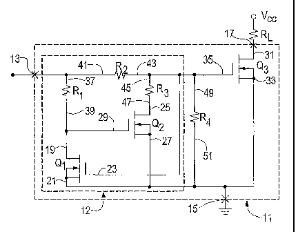
Referring now to Fig. 1, there is shown a first embodiment of a three-terminal
inverting hysteretic transistor switch constructed according to the teachings
of the
present invention, the switch being represented generally by reference numeral
11.
As will be described further in detail below, switch 11 is inverting,
experiences input
signal actuated hysteresis and comprises only three terminals.
Switch 11 comprises an input terminal 13, a ground terminal 15 and an output
terminal 17. As can be appreciated, input terminal 13, ground terminal 15 and
output
terminal 17 are the only terminals for switch 11, which is an object of the
present
invention.
Switch 11 also comprises a first MOSFET Q~, a second MOSFET Q2 and a
third MOSFET Q3. First MOSFET Q,, second MOSFET QZ and third MOSFET Q3 are
identical. Specifically, first MOSFET Q~, second MOSFET Q~ and third MOSFET Q3
are all preferably N-channel, enhancement-mode, VN2222LL-model MOSFETs, each
preferably having a MOSFET threshold voltage VFE-rrH of approximately 1.2
volts.
However, it is to be understood that first MOSFET Q~, second MOSFET Q2 and
third
MOSFET Q3 are not limited to having a threshold voltage of approximately 1.2
volts.
In addition, it is to be understood that first MOSFET Q,, second MOSFET Q2 and
third
MOSFET Q3 are not limited to having equal threshold voltages. Rather, it is to
be
understood that first MOSFET Q~, second MOSFET Q2 and third MOSFET Q3 could
each have different threshold voltage values from one another without
departing from
the spirit of the present invention.
First MOSFET Q~ includes a drain electrode 19, a source electrode 21
connected to ground and a gate electrode 23. Second MOSFET Q2 includes a drain
electrode 25, a source electrode 27 connected to ground and a gate electrode
29
connected to drain electrode 79 of first MOSFET Q,. Third MOSFET Q3 includes a
drain electrode 31 connected to output terminal 17, a source electrode 33
connected
to ground terminal 15 and a gate electrode 35 connected to gate electrode 23
of first
MOSFET Q,.
8
CA 02417378 2003-O1-24
WO 02/09282 PCT/US00/20203
Switch 11 further comprises a first resistor R,, a second resistor R2 and a
third
resistor R3. First resistor R~ preferably has a value of approximately 120
Kohms and
includes a first terminal 37 connected to input terminal 13 and a second
terminal 39
connected to drain electrode 19 of first MOSFET Q,. Second resistor R2
preferably
has a value of approximately 120 Kohms and includes a first terminal 41
connected
to input terminal 13 and a second terminal 43 connected to gate electrode 23
of first
MOSFET Q,. Third resistor R3 preferably has a value of approximately 120 Kohms
and includes a first terminal 45 connected to gate electrode 23 of first
MOSFET Q~
and a second terminal 47 connected to drain electrode 25 of second MOSFET Q2.
Switch 11 additionally comprises a fourth resistor R4. Fourth resistor R4
preferably has a value of approximately 1.0 Mohms and includes a first
terminal 49
connected to gate electrode 23 of first MOSFET Q, and a second terminal 51
connected to ground. It should be noted that fourth resistor R4 is required
because
first MOSFET Q,, second MOSFET Q2 and third MOSFET Q3 are identical. However,
if first MOSFET Q~, second MOSFET Q2 and third MOSFET Q3 had unequal
threshold voltage values which would result in second MOSFET Q~ turning on at
a
lower input voltage than first MOSFET Q, and third MOSFET Q3 during use,
fourth
resistor R4 could be eliminated from switch 11 without departing from the
spirit of the
present invention.
Output terminal 17 can be connected through a load resistor R~ to a supply
voltage V~~, load resistor R~ preferably having a value of 1.0 Kohms. As can
be
appreciated, both load resistor R~ and supply voltage V~~ are external to
switch 11
and consequently are not to be considered part of the present invention.
It should be noted that an additional device, such as a diode, PNP bipolar
transistor, P-channel FET, or programmable unijunction transistor (PUT), could
optionally be connected to input terminal 13 and gate electrode 35 in parallel
with
second resistor R2 without departing from the spirit of the present invention.
As can
be appreciated, the device would serve to assist in removing charge from gate
electrode 35of third MOSFET Q3.
9
CA 02417378 2003-O1-24
WO 02/09282 PCT/US00/20203
Together, first MOSFET Q~, second MOSFET Q~, first resistor R,, second
resistor R~ and third resistor R3 form a hysteresis circuit 12 for third
MOSFET Q3.
Specifically, third MOSFET Q3 acts as the output switch for switch 11.
Hysteresis
circuit 12 provides a high threshold voltage to gate electrode 35, commonly
referred
to as the rising or positive threshold voltage, to switch third MOSFET Q3 on
during
low-to-high input signal transitions and a lower threshold voltage to gate
electrode 35,
commonly referred to as the falling or negative threshold voltage, to switch
third
MOSFET Q3 off during high-to-low input signal transitions, as will be
described in
detail below.
In use, switch 11 functions in the following manner. Fig. 2 represents a
graphical representation comparing an input voltage signal V;" with an output
voltage
signal Vo~t for switch 11, the graphical representation having a vertical axis
53
representing voltage and a horizontal axis 55 representing time. Fig. 3
represents
a chart showing the switching state of first, second and third MOSFETs Q~, QZ
and
Q3 at selected points for input voltage signal V;~. Referring to Figs. 1-3,
with input
voltage V;~ representing a trapezoidal wave and with the time at zero, input
voltage
V;~ is at zero. With input voltage V;n at zero, first MOSFET Q,, second MOSFET
Q2
and third MOSFET Q3 are all off. With third MOSFET Q3 off, no current passes
through load resistor RL. As a result, output voltage Vo"t at output terminal
17 will be
approximately V~~, discarding any leakage.
As input voltage V;" is slowly increased, once input voltage V;" equals 1.0 x
MOSFET threshold voltage VFE-rrH (approximately 1.2 volts), second MOSFET Q2
will
turn on because, with virtually no current in first resistor R~, the voltage
at gate
electrode 29 of second MOSFET Q~ is approximately the value of input voltage
V;n.
Once input voltage V;~ equals MOSFET threshold voltage VFE-,-rH, second MOSFET
Qa will have the value of MOSFET threshold voltage VFE-r-J.H at gate electrode
29 and,
as a consequence, second MOSFET Q2 will turn on, with first MOSFET Q~ and
third
MOSFET Q3 remaining oft. Once second MOSFET QZ turns on, current will flow
through second resistor R~ and third resistor R3. Second resistor RZ and third
resistor
R3 together act as voltage dividers. As a result, voltage at the junction of
second
CA 02417378 2003-O1-24
WO 02/09282 PCT/US00/20203
resistor RZ and third resistor R3 will then pass into gate electrodes 23 and
35 of first
and third MOSFETs Q, and Q3, respectively, with gate electrode 35 of third
MOSFET
Q3 receiving approximately '/2 of input voltage V;n and gate electrode 23 of
first
MOSFET Q~ also receiving approximately ~/z of input voltage V;n.
As input voltage V;~ increases, eventually first and third MOSFETs Q, and Q3
will turn on once input voltage V;~ equals approximately 2.1 x MOSFET
threshold
voltage VFETTH (approximately 2.5 volts), this value of V;~ being identified
as the rising
threshold voltage VTH+ for switch 11 in Fig. 2. When first MOSFET Q, turns on,
first
MOSFET Q~ pulls down the voltage at gate electrode 29 of second MOSFET QZ
until
second MOSFET Q2 turns off. With second MOSFET Q2 off, no current flows
through
third resistor R3. As a consequence, the voltage at gate electrode 35 of third
MOSFET Q3 will rise from approximately 1.0 x MOSFET threshold voltage VFe-rTH
to
approximately 1.9 x MOSFET threshold voltage VFEnH. As a result, switch 11
abruptly turns on, thereby causing rising threshold hysteresis for switch 11
which
causes output voltage Vout to drop to approximately zero volts, as shown in
Fig. 2.
As input voltage V;~ begins to drop at the tail end of the trapezoidal
waveform,
third MOSFET Q3 will turn off once input voltage V;~ equals approximately 1.1
x
MOSFET threshold voltage VFE-~TH (approximately 1.3 volts), this value of V;n
being
identified as the falling threshold voltage VTH_ for switch 11 in Fig. 2.
Specifically, due
to the specific values of second resistor Rz and fourth resistor R4, once
input voltage
V;~ equals approximately 1.1 x MOSFET threshold voltage VFETTH~ gate 35 at
third
MOSFET Q3 has a voltage of approximately MOSFET threshold voltage VFETTH~
Similarly, once input voltage V;n drops below approximately 1.1 x MOSFET
threshold
voltage VFETTH~ first MOSFET Q3 will turn off. Once first MOSFET Q, turns off,
second
MOSFET Q~ will turn back on. With second MOSFET Q2 back on, the voltage at
gate
electrode 35 of third MOSFET Q3 will lower, thereby making first and third
MOSFETs
Q, and Q3 turn off. Once first and third MOSFETs Q~ and Q3 turn off, output
voltage
Vo~t at output terminal 17 will abruptly return to approximately V~~ , as
shown in Fig.
2, discarding any leakage.
11
CA 02417378 2003-O1-24
WO 02/09282 PCT/US00/20203
It should be noted that rising threshold voltage VTH+ (approximately 2.5
volts)
is significantly higher than the falling threshold voltage VTH_ (approximately
1.3 volts),
as shown in Fig. 2. As a result, a noisy input voltage signal V;~ will not
cause switch
11 to experience unwanted state changes, which is desirable.
Referring now to Fig.4, there is shown a second embodiment of a three-
terminal inverting hysteretic transistor switch constructed according to the
teachings
of the present invention, the switch being identified as reference numeral
111. Switch
111 is similar to switch 11 in that switch 111 is also inverting, experiences
input signal
actuated hysteresis and comprises only three terminals.
The principle distinction between switch 111 and switch 11 is that switch 111
comprises a first bipolar junction transistor (BJT) Q,o,, a second bipolar
junction
transistor (BJT) Q~o2 and a third bipolar junction transistor (BJT) Q~03 in
place of first
MOSFET Q~, second MOSFET Q2 and third MOSFET Q3, respectively, of switch 11.
In use, switch 11 and switch 111 function in a similar manner.
It should be noted that although switch 11 is shown comprising three
MOSFETs and switch 111 is shown comprising three bipolar junction transistors,
additional switch embodiments which comprise combinations of MOSFETs and
bipolar junction transistors could readily be manufactured without departing
from the
spirit of the present invention.
Switch 111 comprises an input terminal 113, a ground terminal 115 and an
output terminal 117. As can be appreciated, input terminal 113, ground
terminal 115
and output terminal 117 are the only terminals for switch 111, which is an
object of
the present invention.
First bipolar junction transistor (BJT) Q~01, second bipolar junction
transistor
(BJT) Q~o2 and third bipolar junction transistor (BJT) Q~o3 are identical.
Specifically,
first bipolar junction transistor (BJT) Q,o,, second bipolar junction
transistor (BJT) Qzo2
and third bipolar junction transistor (BJT) Q,o3 are all preferably NPN 2N2222-
type
bipolar junction transistors, each preferably having a BJT threshold voltage
Vg~-,-rH of
approximately 0.7 volts. However, it is to be understood that first BJT Q,o,,
second
BJT Q,o2 and third BJT Q~o3 are not limited to having a threshold voltage of
12
CA 02417378 2003-O1-24
WO 02/09282 PCT/US00/20203
approximately 0.7 volts. In addition, it is to be understood that first BJT
Q,o,, second
BJT Q~o2 and third BJT Q,o3 are not limited to having equal threshold
voltages.
Rather, it is to be understood that first BJT Q,o,, second BJT Q,o2 and third
BJT Q~o3
could each have different threshold voltage values from one another without
departing from the spirit of the present invention.
First BJT Q~o~ includes a collector electrode 119, an emitter electrode 121
connected to ground and a base electrode 123. Second BJT Q~o~ includes a
collector
electrode 125, an emitter electrode 127 connected to ground and a base
electrode
129 connected collector electrode 119 of first BJT Q,o~. Third BJT Q~o3
includes a
collector electrode 131 connected to output terminal 117, an emitter electrode
133
connected to ground terminal 115 and a base electrode 135.
Switch 111 further comprises a first resistor R~01, a second resistor R,o2 and
a
third resistor R,o3. First resistor R~01 preferably has a value of
approximately 1.0
Mohms and includes a first terminal 137 connected to input terminal 113 and a
second terminal 139 connected to collector electrode 119 of first BJT Q~o~.
Second
resistor R~o~ preferably has a value of approximately 22 Kohms and includes a
first
terminal 141 connected to input terminal 113 and a second terminal 143
connected
to base electrode 135 of third BJT Q~o3. Third resistor R~03 preferably has a
value of
approximately 120 Kohms and includes a first terminal 145 connected to base
electrode 135 of third BJT Q,o3 and a second terminal 147 connected to
collector
electrode 125 of second BJT Q,oz
Switch 111 additionally comprises a fourth resistor R,04. Fourth resistor R~04
preferably has a value of approximately 120 Kohms and includes a first
terminal 149
connected to base electrode 135 of third BJT Q~o3 and a second terminal 151
connected to ground. It should be noted that fourth resistor R,04 is required
because
first BJT Q,o~, second BJT Q~o~ and third BJT Q,o3 are identical. However, if
first BJT
Q101~ second BJT Q~o2 and third BJT Q,o3 had unequal turn-on threshold voltage
values which would result in second BJT Q,o~ turning on before first BJT Q,o,
and
third BJT Q,o3 during use, fourth resistor R,o4 could be eliminated from
switch 111
without departing from the spirit of the present invention.
13
CA 02417378 2003-O1-24
WO 02/09282 PCT/US00/20203
Output terminal 117 can be connected through a load resistor R~ to a supply
voltage V~~, load resistor R~ preferably having a value of 1.OKohms. As can be
appreciated, both load resistor R~ and supply voltage V~~ are external to
switch 111
and consequently are not to be considered part of the present invention.
Switch 111 further comprises a fifth resistor R,05. Fifth resistor R,05
preferably
has a value of approximately 1.0 Mohms and includes a first terminal 153
connected
to base electrode 135 of third BJT Q~o3 and a second terminal 155 connected to
base
electrode 123 of first BJT Q,o~. However, it should be noted that if the
current flowing
into base electrode 123 of first BJT Q,o, does not reduce the amount of
current
available to drive base electrode 135 of third BJT Q,o3 to less current than
is needed
for third BJT Q~o3 to switch the load current fihrough load resistor R, and
thus ensure
proper operation of switch 111, fifth resistor R~05 could alternatively have a
value of
zero ohms without departing from the spirit of the present invention. If fifth
resistor
8105 has a value of zero ohms, first terminal 153 and second terminal 155 are
connected together.
It should be noted that an additional device, such as a diode, PNP bipolar
transistor, P-channel FET, or programmable unijunction transistor (PUT), could
optionally be connected to input terminal 113 and base electrode 135 in
parallel with
second resistor R~o2 without departing from the spirit of the present
invention. As can
be appreciated, the device would serve to assist in removing charge from base
electrode 135 of third BJT Q~o3.
In use, switch 111 functions in a similar manner to switch 11. In particular,
switch 111 similarly has a rising threshold voltage which is significantly
higher than
its falling threshold voltage, as shown in Fig. 5. As a result, a noisy input
signal will
not cause switch 111 to experience unwanted state changes, which is desirable.
Referring now to Fig.6, there is shown a third embodiment of a three-terminal
inverting hysteretic transistor switch constructed according to the teachings
of the
present invention, the switch being identified as reference numeral 211.
Switch 211
is similar to switch 111 in that switch 211 is also inverting, experiences
input signal
actuated hysteresis and comprises only three terminals.
14
CA 02417378 2003-O1-24
WO 02/09282 PCT/US00/20203
Switch 211 is similar to switch 111 in that switch 211 comprises an input
terminal 213, a ground terminal 215 and an output terminal 217. As can be
appreciated, input terminal 213, ground terminal 215 and output terminal 217
are the
only terminals for switch 211, which is an object of the present invention.
Switch 211 is similar to switch 111 in that switch 211 comprises a first
bipolar
junction transistor (BJT) Q2o, and a second bipolar junction transistor (BJT)
Q~o2 which
are identical in construction with first BJT Q,o, and second BJT Q,o2 of
switch 111.
Preferably, first BJT Q2o~ and second BJT Q2o2 are both NPN 2N2222-type
bipolar
junction transistors, each preferably having a BJT threshold voltage VB~TTH of
approximately 0.7 volts. However, it is to be understood that first BJT Q2o~
and
second BJT Q2o~ are not limited to having a threshold voltage of approximately
0.7
volts. In addition, it is to be understood that first BJT Q2o, and second BJT
Q2o2 are
not limited to having equal threshold voltages. Rather, it is to be understood
that first
BJT Q2o~ and second BJT Q2o2 could each have different threshold voltage
values
from one another without departing from the spirit of the present invention.
First BJT Q2o~ includes a collector electrode 219, an emitter electrode 221
connected to ground and a base electrode 223. Second BJT Q~o2 includes a
collector
electrode 225, an emitter electrode 227 connected to ground and a base
electrode
229 connected to collector electrode 219 of first BJT Q2o~.
Switch 211 also comprises a first resistor Rio,, a second resistor R2o2 and a
third resistor R2oa. First resistor R~o~ preferably has a value of
approximately 1.0
Mohms and includes a first terminal 231 connected to input terminal 213 and a
second terminal 233 connected to collector electrode 219 of first BJT Q2o,.
Second
resistor R~o2 preferably has a value of approximately 120 Kohms and includes a
first
terminal 235 connected to input terminal 213 and a second terminal 237. Third
resistor Rzos preferably has a value of approximately 1.0 Mohms and includes a
first
terminal 239 connected to second terminal 237 of second resistor R2o~ and a
second
terminal 241 connected to collector terminal 225 of second BJT Q2o2.
The principle distinction between switch 211 and switch 111 is that switch 211
comprises a Darlington-connected compound bipolar junction transistor Q2os in
place
CA 02417378 2003-O1-24
WO 02/09282 PCT/US00/20203
of third BJT Q~o3 of switch 111. Darlington-connected compound BJT Q2os is
desirable in that it has twice the turn-on threshold voltage of either first
BJT Q2o, or
second BJT Q2o2. As a consequence, no resistor is required in switch 211 to
perform
the function performed by fourth resistor R,04 in switch 111. Darlington-
connected
compound BJT Q2os is also desirable because it can switch relatively high
current and
voltage with small die area.
Darlington-connected compound BJT Q2os comprises a fourth BJT Q2o4 and a
fifth BJT Q2o5. Preferably, fourth BJT Q2o4 and fifth BJT Q2o5 are both NPN
TIP121-
type bipolar junction transistors, each preferably having a BJT threshold
voltage
1O Vg~TTH of approximately 1.4 volts or approximately two times the voltage of
the
threshold voltage of first BJT Q2o~ and second BJT Q2o2.
Fourth BJT Q2o4 includes a collector electrode 243 connected to output
terminal 217, an emitter electrode 245 and a base electrode 247 connected to
second terminal 237 of second resistor RZO2. Fifth BJT Q2os includes a
collector
electrode 249 connected to output terminal 217, an emitter electrode 251
connected
to ground and a base electrode 253 connected to emitter electrode 245 of
fourth BJT
Q204
Switch 111 additionally comprises a fourth resistor R2o4 and a fifth resistor
R2os
which together act as a resistor divider for increasing the effective turn-on
voltage
threshold of first BJT Q2o~. Fourth resistor R2o4 preferably has a value of
approximately 1.0 Mohms and includes a first terminal 257 connected to base
electrode 247 of fourth BJT Q2o4 and a second terminal 259 connected to base
electrode 223 of first BJT Q2o~. Fifth resistor R2o5 preferably has a value of
approximately 1.0 Mohms and includes a first terminal 261 connected to second
terminal 259 of fourth resistor R2o4 and a second terminal 263 connected to
ground.
Output terminal 217 can be connected through a load resistor R~ to a supply
voltage V~~, load resistor R~ preferably having a value of 1.OKohms. As can be
appreciated, both load resistor R~ and supply voltage V~~ are external to
switch 211
and consequently are not to be considered part of the present invention.
16
CA 02417378 2003-O1-24
WO 02/09282 PCT/US00/20203
It should be noted that an additional device, such as a diode, PNP bipolar
transistor, P-channel FET, or programmable unijunction transistor (PUT), could
optionally be connected to input terminal 213 and base electrode 247 in
parallel with
second resistor R2o2 without departing from the spirit of the present
invention. As can
be appreciated, the device would serve to assist in removing charge from base
electrode 247 of fourth BJT QZOa.
In use, switch 211 functions in a similar manner to switch 111. In particular,
switch 211 similarly has a rising threshold voltage which is significantly
higher than
its falling threshold voltage. As a result, a noisy input signal will not
cause switch 211
to experience unwanted state changes, which is desirable.
Referring now to Fig.7, there is shown a fourth embodiment of a three-terminal
inverting hysteretic transistor switch constructed according to the teachings
of the
present invention, the switch being identified as reference numeral 311.
Switch 311
is similar to switch 11 in that switch 311 is also inverting, experiences
input signal
actuated hysteresis and comprises only three terminals.
Switch 311 comprises an input terminal 313, a ground terminal 315 and an
output terminal 317. As can be appreciated, input terminal 313, ground
terminal 315
and output terminal 317 are the only terminals for switch 311, which is an
object of
the present invention.
Switch 311 differs principally from switch 11 in that switch 311 comprises a
hysteresis circuit 312 which differs in construction from hysteresis circuit
12, as will
be described further in detail below.
Switch 311 comprises a first MOSFET Q3o,, a second MOSFET Q3o~, a third
MOSFET Q3os, a fourth MOSFET Q3oa and a fifth MOSFET Q3o5. First MOSFET Q3o,,
second MOSFET Q3o~, third MOSFET Q3os and fourth MOSFET Q3o4 are all
preferably
N-channel, enhancement-mode MOSFETs, each preferably having a MOSFET
threshold voltage VFE-r-,.H of approximately 1.2 volts. Fifth MOSFET Q3os is
preferably
a P-channel enhancement-mode MOSFET having a MOSFET threshold voltage
VFETfH Of approximately 1.2 volts. However, it is to be understood that first
MOSFET
~301~ second MOSFET Q3o2, third MOSFET Q3o3, fourth MOSFET Q3oa and fifth
17
CA 02417378 2003-O1-24
WO 02/09282 PCT/US00/20203
MOSFET Q3os are not limited to having a threshold voltage of approximately 1.2
volts.
In addition, it is to be understood that first MOSFET Q3o~, second MOSFET
Q3o2,third
MOSFET Q3o3, fourth MOSFET Q3o4 and fifth MOSFET Q3os are not limited to
having
equal threshold voltages. Rather, it is to be understood that first MOSFET
Q3o~,
second MOSFET Q3o~, third MOSFET Q3o3, fourth MOSFET Q3oa and fifth MOSFET
Q305 could each have different threshold voltage values from one another
without
departing from the spirit of the present invention.
First MOSFET Q3o~ includes a drain electrode 319, a source electrode 321
connected to ground terminal 315 and a gate electrode 323. Second MOSFET Q3o2
includes a drain electrode 325, a source electrode 327 connected to ground
terminal
315 and a gate electrode 329. Third MOSFET Q3os includes a drain electrode 331
connected to output terminal 317, a source electrode 333 connected to ground
terminal 315 and a gate electrode 335. Fourth MOSFET Q3oa includes a drain
electrode 337 connected to gate electrode 335 of third MOSFET Q3o3, a source
electrode 339 connected to ground terminal 315 and a gate electrode 341
connected
to gate electrode 323 of first MOSFET Q3o~. Fifth MOSFET Q3os includes a drain
electrode 343 connected to gate electrode 335 of third MOSFET Q3o3, a source
electrode 345 connected to input terminal 313 and a gate electrode 347
connected
to drain electrode 325 of second MOSFET Q3o~.
Switch 311 further comprises a first resistor R3o~, a second resistor R3o2 and
a
third resistor R3o3. First resistor R3o, preferably has a value of
approximately 1.0
Mohms and includes a first terminal 349 connected to input terminal 313 and a
second terminal 351 connected to gate electrode 329 of second MOSFET Q2.
Second resistor R3oz preferably has a value of approximately 1.0 Mohms and
includes
a first terminal 353 connected to input terminal 313 and a second terminal 355
connected to gate electrode 347 of fifth MOSFET Q3os. Third resistor 8303
preferably
has a value of approximately 1.0 Mohms and includes a first terminal 357
connected
to gate electrode 329 of second MOSFET Q3o2 and a second terminal 359
connected
to drain electrode 359 of first MOSFET Q3o,.
18
CA 02417378 2003-O1-24
WO 02/09282 PCT/US00/20203
Switch 311 additionally comprises a fourth resistor R3oa- Fourth resistor R3o4
preferably has a value of approximately 1.0 Mohms and includes a first
terminal 361
connected to gate electrode 335 of third MOSFET Q3oa and a second terminal 363
connected to ground terminal 315. It should be noted that fourth resistor R3oa
is not
essential to the function of switch 311 and accordingly, could be removed
without
departing from the spirit of the present invention; However, removal of fourth
resistor
8304 is not preferred because removal of fourth resistor R3o4 may degrade the
capability of third MOSFET Q3oa to turn off in some situations.
Output terminal 317 can be connected through a load resistor R~ to a supply
voltage V~~, load resistor R~ preferably having a value of 1.0 Kohms. As can
be
appreciated, both load resistor R~ and supply voltage V~~ are external to
switch 311
and consequently are not to be considered part of the present invention.
It should be noted that an additional device, such as a diode, PNP bipolar
transistor, P-channel FET, or programmable unijunction transistor (PUT), could
optionally be connected to input terminal 313 and drain electrode 343 of fifth
MOSFET Q3o5 without departing from the spirit of the present invention. As can
be
appreciated, the device would serve to assist in removing charge from gate
electrode
335 of third MOSFET Q3o3.
In use, switch 311 functions similarly to switch 11. Specifically, third
MOSFET
Q303 acts as the output switch for switch 311. Together, first MOSFET Q3o~,
second
MOSFET Q3oz, fourth MOSFET Q3o4, fifth MOSFET Q3o5, first resistor R3o~,
second
resistor R3o2, third resistor R3os and fifth resistor R3os form hysteresis
circuit 312 for
third MOSFET Q3o3. Hysteresis circuit 312 provides a high threshold voltage to
gate
electrode 335, commonly referred to as the rising or positive threshold
voltage, to
switch third MOSFET Q3os on during low-to-high input signal transitions and a
lower
threshold voltage to gate electrode 335, commonly referred to as the falling
or
negative threshold voltage, to switch third MOSFET Q3os off during high-to-low
input
signal transitions. Because switch 311 has a rising threshold voltage which is
significantly higherthan its falling threshold voltage, a noisy input signal
will not cause
switch 311 to experience unwanted state changes, which is desirable.
19
CA 02417378 2003-O1-24
WO 02/09282 PCT/US00/20203
It should be noted that, due to its complex arrangement, hysteresis circuit
312
is a higher performance circuit than hysteresis circuit 12 of switch 11.
Specifically,
hysteresis circuit 312 is preferable because hysteresis circuit 312 improves
the turn-
off of third MOSFET Q3o3 through the gate charge path and because hysteresis
circuit
312 enables nearly the entire input voltage V;n to be applied directly to
third MOSFET
~303~
Referring now to Fig.B, there is shown a fifth embodiment of a three-terminal
inverting hysteretic transistor switch constructed according to the teachings
of the
present invention, the switch being identified as reference numeral 411.
Switch 411
is similar to switch 311 in that switch 411 is also inverting, experiences
input signal
actuated hysteresis and comprises only three terminals.
Switch 411 is similar to switch 311 in that switch 411 comprises an input
terminal 413, a ground terminal 415 and an output terminal 417. As can be
appreciated, input terminal 413, ground terminal 415 and output terminal 417
are the
only terminals for switch 411, which is an object of the present invention.
Switch 411 differs principally from switch 311 in that switch 411 comprises an
integrated circuit (IC) chip U, in place of hysteresis circuit 312.
IC chip U~ is a voltage detector CMOS IC chip, such as Panasonic IC chip,
model MN13812(G), or Motorola IC chip, model MC33464-XX. IC chip U, includes
a input voltage pin Vpp which is connected to input terminal 413, a ground pin
GND
which is connected to ground terminal 415 and an output pin OUT.
Switch 411 comprises a MOSFET Q4o3 which is preferably an N-channel,
enhancement-mode, VN2222LL-model MOSFET. MOSFET Q4o3 includes a drain
electrode 419 connected to output terminal 417, a source electrode 421
connected
to ground terminal 415 and a gate electrode 423 connected to output pin OUT of
IC
chip U,.
Switch additionally comprises a resistor R4o4 which preferably has a value of
approximately 1.0 Mohms and includes a first terminal 425 connected to gate
electrode 423 of MOSFET Q4o3 and a second terminal 427 connected to ground
terminal 415. It should be noted that fourth resistor R4oa is not essential to
the
CA 02417378 2003-O1-24
WO 02/09282 PCT/US00/20203
function of switch 411 and accordingly, could be removed without departing
from the
spirit of the present invention; However, removal of fourth resistor R4o4 is
not preferred
because removal of fourth resistor R4oa may degrade the capability of MOSFET
Q4oa
to turn off in some situations.
Output terminal 417 can be connected through a load resistor R~ to a supply
voltage V~~, load resistor R~ preferably having a value of 1.OKohms. As can be
appreciated, both load resistor R~ and supply voltage V~~ are external to
switch 411
and consequently are not to be considered part of the present invention.
It should be noted that an additional device, such as a diode, PNP bipolar
transistor, P-channel FET, or programmable unijunction transistor (PUT), could
optionally be connected to input terminal 413 and gate electrode 423 without
departing from the spirit of the present invention. As can be appreciated, the
device
would serve to assist in removing charge from gate electrode 423 of MOSFET
Q4o3.
In use, switch 411 functions in a similar manner to switch 311. In particular,
switch 411 similarly has a rising threshold voltage which is significantly
higher than
its falling threshold voltage. As a result, a noisy input signal will not
cause switch 411
to experience unwanted state changes, which is desirable.
Referring now to Fig.9, there is shown a sixth embodiment of a three-terminal
inverting hysteretic transistor switch constructed according to the teachings
of the
present invention, the switch being identified as reference numeral 511.
Switch 511
is similar to switch 311 in that switch 511 is also inverting, experiences
input signal
actuated hysteresis and comprises only three terminals.
Switch 511 is similar to switch 311 in that switch 511 comprises an input
terminal 513, a ground terminal 515 and an output terminal 517. As can be
appreciated, input terminal 513, ground terminal 515 and output terminal 517
are the
only terminals for switch 511, which is an object of the present invention.
Switch 511 differs principally from switch 311 in that switch 511 comprises an
integrated circuit (IC) chip U2, a capacitor C, a diode D, and a first MOSFET
QSO, in
place of hysteresis circuit 312.
21
CA 02417378 2003-O1-24
WO 02/09282 PCT/US00/20203
IC chip U2 is a voltage detector CMOS IC chip, such as Motorola IC chip,
model MC33465-XX. IC chip U2 includes a input voltage pin Vpp which is
connected
to input terminal 513, a ground pin GND which is connected to ground terminal
415,
a reset pin RESET and an output pin CD.
Capacitor C is preferably a 1000 pF capacitor and includes a first terminal
519
connected to output pin CD of IC chip U2 and a second terminal 521. Diode D
includes a first terminal 523 connected to second terminal 521 of capacitor C
and a
second terminal 525 connected to ground terminal 515.
First MOSFET QSO, is preferably an N-channel, depletion-mode MOSFET and
includes a drain electrode 527 connected to reset pin RESET of IC chip U2, a
source
electrode 529 connected to ground terminal 515 and a gate electrode 531
connected
to second terminal 521 of capacitor C.
Switch 511 further comprises a second MOSFET QSOa is preferably an N-
channel, enhancement-mode, VN2222LL-model MOSFET. MOSFET QSOS includes
a drain electrode 531 connected to output terminal 517, a source electrode 533
connected to ground terminal 515 and a gate electrode 535 connected to reset
pin
RESET of IC chip U2.
Switch 511 additionally comprises a resistor RSOawhich preferably has a value
of approximately 1.0 Mohms and includes a first terminal 537 connected to gate
electrode 535 of second MOSFET QSOS and a second terminal 539 connected to
ground terminal 515. It should be noted that resistor RSOa is not essential to
the
function of switch 511 and accordingly, could be removed without departing
from the
spirit of the present invention; However, removal of resistor 8504 is not
preferred
because removal of resistor R5o4 may degrade the capability of second MOSFET
Q5os
to turn off in some situations.
Output terminal 517 can be connected through a load resistor R~ to a supply
voltage V~~, load resistor R~ preferably having a value of 1.OKohms. As can be
appreciated, both load resistor R~ and supply voltage V~~ are external to
switch 511
and consequently are not to be considered part of the present invention.
22
CA 02417378 2003-O1-24
WO 02/09282 PCT/US00/20203
It should be noted that an additional device, such as a diode, PNP bipolar
transistor, P-channel FET, or programmable unijunction transistor (PUT), could
optionally be connected to input terminal 513 and gate electrode 535 without
departing from the spirit of the present invention. As can be appreciated, the
device
would serve to assist in removing charge from gate electrode 535 of second
MOSFET Q5o3.
In use, switch 511 functions in a similar manner to switch 311. In particular,
switch 511 similarly has a rising threshold voltage which is significantly
higher than
its falling threshold voltage. As a result, a noisy input signal will not
cause switch 511
to experience unwanted state conditions, which is desirable.
The embodiments of the present invention described above are intended to
be merely exemplary and those skilled in the art shall be able to make
numerous
variations and modifications to it without departing from the spirit of the
present
invention. All such variations and modifications are intended to be within the
scope
of the present invention as defined in the appended claims.
23