Sélection de la langue

Search

Sommaire du brevet 2420119 

Énoncé de désistement de responsabilité concernant l'information provenant de tiers

Une partie des informations de ce site Web a été fournie par des sources externes. Le gouvernement du Canada n'assume aucune responsabilité concernant la précision, l'actualité ou la fiabilité des informations fournies par les sources externes. Les utilisateurs qui désirent employer cette information devraient consulter directement la source des informations. Le contenu fourni par les sources externes n'est pas assujetti aux exigences sur les langues officielles, la protection des renseignements personnels et l'accessibilité.

Disponibilité de l'Abrégé et des Revendications

L'apparition de différences dans le texte et l'image des Revendications et de l'Abrégé dépend du moment auquel le document est publié. Les textes des Revendications et de l'Abrégé sont affichés :

  • lorsque la demande peut être examinée par le public;
  • lorsque le brevet est émis (délivrance).
(12) Brevet: (11) CA 2420119
(54) Titre français: PROCEDE ET DISPOSITIF PERMETTANT DE TESTER LE FONCTIONNEMENT DE CARTES DE CIRCUITS IMPRIMES
(54) Titre anglais: METHOD AND DEVICE FOR TESTING THE OPERATIVES OF PRINTED CIRCUIT BOARDS
Statut: Périmé et au-delà du délai pour l’annulation
Données bibliographiques
(51) Classification internationale des brevets (CIB):
  • G01R 31/309 (2006.01)
  • G01R 31/28 (2006.01)
(72) Inventeurs :
  • STENGEL, JURGEN (Allemagne)
(73) Titulaires :
  • BOTEST SYSTEMS GMBH
(71) Demandeurs :
  • BOTEST SYSTEMS GMBH (Allemagne)
(74) Agent: DEETH WILLIAMS WALL LLP
(74) Co-agent:
(45) Délivré: 2009-12-22
(86) Date de dépôt PCT: 2001-08-01
(87) Mise à la disponibilité du public: 2002-02-14
Requête d'examen: 2006-06-28
Licence disponible: S.O.
Cédé au domaine public: S.O.
(25) Langue des documents déposés: Anglais

Traité de coopération en matière de brevets (PCT): Oui
(86) Numéro de la demande PCT: PCT/EP2001/008882
(87) Numéro de publication internationale PCT: WO 2002012911
(85) Entrée nationale: 2003-02-04

(30) Données de priorité de la demande:
Numéro de la demande Pays / territoire Date
100 38 313.0 (Allemagne) 2000-08-05

Abrégés

Abrégé français

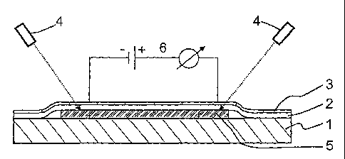
Procédé permettant de tester le fonctionnement de cartes de circuits imprimés, qui consiste à appliquer directement sur au moins une face d'une carte de circuits imprimés (1) une couche souple (2) ne laissant initialement pas passer le courant de manière à établir le contact, ladite couche étant connectée de manière fonctionnelle à un conducteur de courant (3), puis à mettre ladite couche (2) sous tension. Un passage de courant est alors partiellement créé vers les sites de contact qui délimitent une piste conductrice (5) à tester. Le flux de courant dans la piste conductrice (5) est ensuite mesuré par l'intermédiaire du conducteur de courant (3).


Abrégé anglais


A process for testing circuit boards for serviceability is designed such that
a flexible layer (2)
that is initially impermeable to current is placed directly on at least one
side of the circuit
board (1), making contact, and it is dynamically connected to a current
conductor (3), the
layer (2) is then energized and then a current passage is partially created at
the contact points
that delimit the respective conductor path (5) that is to be tested, and then
the flow of current
in the conductor path (5) is measured using the current conductor (3).

Revendications

Note : Les revendications sont présentées dans la langue officielle dans laquelle elles ont été soumises.


Claims
What is claimed is:
1. Process for testing a circuit board for serviceability, characterized in
that a flexible
layer (2) that is initially impermeable to current is placed directly on at
least one side of the
circuit board (1), making contact, and is functionally connected to a current
conductor (3), the
layer (2) is then energized and then a current passage is partially created at
the contact points
that delimit a respective conductor path (5) to be tested, a current passage
is created, and
current flow in the conductor path (5) is measured via the current conductor
(3).
2. Process according to claim 1, wherein the current passage is produced by a
laser
beam that penetrates the layer (2) in the area of the location of the
conductor path (5).
3. Process according to claim 1, wherein a plasma is applied as the layer (2).
4. Process according to claim 1, wherein a polymer film is applied as the
layer (2).
5. Process according to claim 4, wherein the polymer film is photoconductive.
6. Process according to claim 1, wherein the current conductor (3) is applied
to the
entire surface of the layer (2).
7. Device for carrying out the process according to claim 1, wherein there are
transmitters (4) with which one laser beam at a time can be generated by which
a partial
current passage in the layer (2) can be produced.
8. Device according to claim 7, wherein there are mirrors with which the laser
beam
can be deflected.
9. Device according to claim 7, wherein the current conductor (3) consists of
a
transparent, partitioned film, the fields (7) being polarized differently in a
checkerboard
manner.
10. Device according to claim 7, wherein the current conductor (3) consists of
a
polymer film that lies on the side opposite the layer (2) making contact on
the circuit board
(1).
11. Device according to claim 10, wherein the polymer film is photoconductive.
8

12. Device according to claim 7, wherein between the layer (2) and the current
conductor (3), there is a measurement device (6) with which the current flow
through the
conductor path (5) can be measured.
13. Device according to claim 7, wherein the current conductor (3) is made as
a
superficial, transparent electrode that covers the layer (2) at least in the
test area.
14. Device according to claim 12, wherein the current conductors (3) that are
made as
electrodes and the layer (2) are made in one piece.
9

Description

Note : Les descriptions sont présentées dans la langue officielle dans laquelle elles ont été soumises.


CA 02420119 2008-08-08
4048 0002
Method and Device for'Testing the Operatives of Printed Circuit Boards
This itiventiotl relates to a process for testing circuit boards for
serviceability and a
de~ic~; for carrying out the pt-ocess.
To test for serviceabilitv of eireuit boards, i.e. test for current flow
within conductor
paths both on one side of the circuit board and also froni one sicle to the
other, the expression
"bareboard test system" discloses a pt-ocess in which testing for electt-ical
permeability of
coMlLietor paths takes place by elastic contact pins that are attetcbed to
both sides of the circuit
board in a die and are configured in their arrangement according to the
contact points.
In order to ensure reliabie contact of the contact pins with the corresponding
contact
points, the dies are moved with a cet-tain pressure against the circuit board,
and the forces
resulting from the springs of the contact pin must be overcome. For the host
of contact pins
that are conventionally used, considerable pressures that dictate a
corresponding mechanicai
concept are necessary.
The equipment costs that must be borne here lead to considerable production
costs of
one such machine, another disadvantage heing relativeiy great fault
susceptibility that is
caused especially by the large number of contact pins used, which can be in
the range of
10,000 pieces.
The possible density of contact points that increases with newer technologies
linlits
the use of contact pins so that the attainable resolution for making contact
with circuit boards
no longer keeps up with modern requiremcnts.
1

CA 02420119 2003-02-04
4048 0002
Another process is known under the term "flying probetester". Here, 2 to 8
test
needles at a time are positioned on the two sides of the circuit board by
suitable movement
units over the contact points of the circuit board for which the electrical
permeability is to be
determined. Contact-making between the test needles and the selected contact
point on the
circuit board takes place by lowering the test needles onto this point. The
current proceeding
from the first test needle is routed to the circuit board contact, and on the
other end of the
conductor path, it is likewise received and measured by one such test needle.
In principle, it is
testing by contact here, one test needle being assigned to each contact site
of the conductor
path not according to the described contact pins, but their being moved
accordingly,
computer-controlled. Here, there is the danger of damage of the contact points
by multiple
contact, with the consequence that problems in the component placement on the
circuit board
can occur.
In order to avoid this damage, attempts have already been made to replace the
test
needles by a conductive plasma by which contact with the contact points is
established.
The disadvantage here, however, is that the speed within which the circuit
board can
be completely tested is relatively low, in particular based on the working
steps: paired
positioning of the test needles, lowering, measuring and moving to the next
positions. These
test systems rather quickly reach their resolution limits, i.e., operating
limits, due to the size
of the test needles and the only limited possible accuracy of the movement
units.
Finally, US 5 177 437 describes testing of circuit boards in which a matrix
that can be
photoelectrically activated by means of a light source is applied to the glass
plate. Between
the matrix and the circuit board, there is an electrically conductive mat. In
any case, the
2

CA 02420119 2007-11-13
4048 0002
construction cost for executin" tliis process is relatively high. In
adciition, the interc.onnected
nlat anci the nl,ttrix that is ri -id compared to the circttit board cannot
equalize or take into
aCCUlttll prodUCt1U11-lndllCed Llllevetuiess and Inacclu-acies of thc surface
of thc cit-cuit board,
sucll that an absolutely accutate test result is not guaranteed.
For operation, nloreover, there are "light valves" designated as such, by
wllicll the
emitted light beam of a continuous light source is masked and unmasked
according to
requirements. The construction cost here is extrenlely lli.gh arld in addition
to high production
costs, it leads to fault susceptibility that prevents optinntm operation.
Therefore, the object of this invention is to develop a process of the generic
type such
that it can be carried out with low equipment costs and high speed, higher
test accuracy is
achieved, and extremely small contact points of the circuit board can be
tested.
This object is achieved by a process for testing a circuit board for
serviceability,
characterized in that a flexible layer that is initially impermeable to
current is placed directly
on at least one side of the circuit board, making contact, and is functionally
connected to a
current conductor. The layer is then energized and a current passage is
partially created at the
contact points that delimit a respective conductor path to be tested. A
current passage is
created, and current flow in the conductor path is measured via the current
conductor.
The process according to the invention now etlables testing that is extremely
effective
with respect to the working speed and that is nondestntctive at the sanie time
with respect to
the circttit board.
Direct application of a flexible layer to at least one side of the circuit
board, i.e., direct
contact-nlaking, on the one lland makes the structural cost nluch lowet' than
in the kno-vvn
processes, ancl. on the other hand, ensures that produc.tion-induced
unevenness of the circuit
board is also taken into accotlnt. The layer that is initially inlpermeable to
cttrt-cnt rests
directly on each point of the circuit board based on its flexible
cotllposition, so that almost no
tcst inaccuraciCs arisc. The lluality of tlle test result is thus much
improvcd. 'I'llis is tlicr-efore
espeeially notcNVorthy when thcse circuit bWRIy MV used in large nunlbers, and
theretore the
3

CA 02420119 2003-02-04
4048 0002
highest possible quality assurance, which includes optimum testing, is what is
important.
Current passage can be produced by a laser beam that proceeds from a static
source.
The beam is deflected by tiny and extremely light mirrors, so that in the
positioning of the
beam, only a small mass need be moved into the area of contact of the
conductor path to be
tested; as mentioned, the process can be carried out much more quickly than is
possible in the
described prior art.
As the layers that can be applied to the two sides of the circuit board, they
can be
applied from a plasma that fills a space that is bordered on one side by the
circuit board and
that is otherwise sealed to such an extent that this plasma cannot flow in.
Here, the plasma has the advantage that it is ionized solely in the area
produced by the
laser beam, and it becomes electrically conductive.
To determine the permeability of a conductor path that is located on one side
of the
circuit board, a partitioned layer can be applied that represents a current
conductor and that is
made alternatingly in the partitions such that in conjunction with the
conductor path that is
under the plasma layer when serviceability is perfect, a circuit is formed
that can be
determined by means of a connected measurement device.
According to another idea of the invention, it is provided that on one side of
the
circuit board a film be placed that represents an equivalent to the indicated
plasma layer and
on which a partitioned layer is also placed comparably thereto. This layer can
be
photoconductive and can consist of, for example, organic semiconductors
(special polymers).
By applying film to the two sides of the circuit board, the permeability of
the
conductor paths that are routed through the circuit board and that have
contact points on each
4

CA 02420119 2003-02-04
4048 0002
side can be tested. Here, partitioning of the films can be abandoned since the
latter jointly
form a circuit in which the measurement device is located at a suitable
location. In order to
be able to check a conductor path provided on one side with strip conductors
in this
arrangement, a partitioned film is feasibly used.
A suitable film is a so-called polymer film that becomes conductive in the
area
irradiated by the laser beam, but impermeable to current again in this area
directly after the
laser beam is turned off.
This makes it possible to position the laser beam in a very short time
sequence at the
most varied points so that current can flow through the individual contact
points of the circuit
board without difficulty. In the case in which this contact point is faulty,
i.e., no current is
flowing, this is indicated by the measurement technology that is integrated
into the circuit.
It can be established at any time, for example by keeping a record, at which
contact
position the circuit board is faulty.
Other advantageous further developments of the invention are identified in the
subclaims.
The process according to the invention and a device for carrying out the
process are
described below using the attached drawings.
Here:
Figure 1 shows an embodiment of a device for carrying out the process in a
schematic side view,
Figure 2 shows another embodiment of one such device likewise in a schematic
side view,
5

CA 02420119 2003-02-04
4048 0002
Figure 3 shows a schematic overhead view of the device according to Figure 2.
Figure 1 shows a device with which circuit boards 1 can be tested for
serviceability.
In doing so, current passage through a conductor path 5 that is routed
transversely
through the circuit board 1 is determined so that on both sides of the circuit
board 1, there are
contact points that border the conductor path 5.
On the opposing sides of the circuit board 1, one flexible layer 2 that is
initially
impermeable to current in the form of a polymer film is applied at a time,
making contact, of
which each is connected to one of the two poles of a voltage source.
Between the transparent layers 2 and the contact points to be tested on the
circuit
board 1, an electrical field is built up by the applied voltage.
On both sides, there is a transmitter 4 with which a laser beam is produced
and
preferably deflected and which penetrates the respectively assigned layer 2 in
an area of its
beam diameter.
In this area, the layer 2 is then permeable to current so that in the case in
which the
conductor path 5 is not damaged, the circuit is closed.
A measurement-source device 6 is located between the two layers, connecting
them,
in order, on the one hand, to apply a voltage difference, and, on the other
hand, to ascertain
whether current is flowing through the conductor path 5 or not.
Figures 2 and 3 show a device with which a conductor path 5 that is provided
only on
one side of the circuit board 1 is tested for permeability.
At least in the test area, a current conductor 3 in the form of a layer is
applied to the
layer 2, preferably making contact as a superficial, transparent electrode,
which enables
6

CA 02420119 2003-02-04
4048 0002
unhindered passage of the laser beam that is shown by the broken line, and
that can be made
integral with the photoconductive layer 2. In this case, the current conductor
3, i.e., the
electrode, forms a carrier layer for the layer 2.
As Figure 3 especially clearly shows, the current conductor 3 is partitioned
into fields
7 that are arranged in a checkerboard manner with different poles, a
differently polarized field
7 being assigned to each contact area bordering the conductor path 5.
In this way, a conductor circuit is built up to which is connected the
measurement-
source device 6 by which the permeability of the conductor path 5 can be
determined.
7

Dessin représentatif
Une figure unique qui représente un dessin illustrant l'invention.
États administratifs

2024-08-01 : Dans le cadre de la transition vers les Brevets de nouvelle génération (BNG), la base de données sur les brevets canadiens (BDBC) contient désormais un Historique d'événement plus détaillé, qui reproduit le Journal des événements de notre nouvelle solution interne.

Veuillez noter que les événements débutant par « Inactive : » se réfèrent à des événements qui ne sont plus utilisés dans notre nouvelle solution interne.

Pour une meilleure compréhension de l'état de la demande ou brevet qui figure sur cette page, la rubrique Mise en garde , et les descriptions de Brevet , Historique d'événement , Taxes périodiques et Historique des paiements devraient être consultées.

Historique d'événement

Description Date
Le délai pour l'annulation est expiré 2015-08-03
Lettre envoyée 2014-08-01
Accordé par délivrance 2009-12-22
Inactive : Page couverture publiée 2009-12-21
Inactive : Taxe finale reçue 2009-09-16
Préoctroi 2009-09-16
Un avis d'acceptation est envoyé 2009-06-22
Lettre envoyée 2009-06-22
Un avis d'acceptation est envoyé 2009-06-22
Inactive : Approuvée aux fins d'acceptation (AFA) 2009-06-18
Modification reçue - modification volontaire 2008-08-08
Inactive : Dem. de l'examinateur par.30(2) Règles 2008-07-04
Déclaration du statut de petite entité jugée conforme 2008-06-19
Requête visant une déclaration du statut de petite entité reçue 2008-06-19
Modification reçue - modification volontaire 2007-11-13
Inactive : Dem. de l'examinateur par.30(2) Règles 2007-09-04
Modification reçue - modification volontaire 2006-09-28
Lettre envoyée 2006-08-21
Exigences pour une requête d'examen - jugée conforme 2006-06-28
Toutes les exigences pour l'examen - jugée conforme 2006-06-28
Requête d'examen reçue 2006-06-28
Inactive : CIB de MCD 2006-03-12
Lettre envoyée 2003-07-14
Inactive : Transfert individuel 2003-06-10
Inactive : Lettre de courtoisie - Preuve 2003-06-03
Inactive : Page couverture publiée 2003-05-30
Inactive : Notice - Entrée phase nat. - Pas de RE 2003-05-28
Demande reçue - PCT 2003-03-24
Exigences pour l'entrée dans la phase nationale - jugée conforme 2003-02-04
Déclaration du statut de petite entité jugée conforme 2003-02-04
Demande publiée (accessible au public) 2002-02-14

Historique d'abandonnement

Il n'y a pas d'historique d'abandonnement

Taxes périodiques

Le dernier paiement a été reçu le 2009-06-22

Avis : Si le paiement en totalité n'a pas été reçu au plus tard à la date indiquée, une taxe supplémentaire peut être imposée, soit une des taxes suivantes :

  • taxe de rétablissement ;
  • taxe pour paiement en souffrance ; ou
  • taxe additionnelle pour le renversement d'une péremption réputée.

Veuillez vous référer à la page web des taxes sur les brevets de l'OPIC pour voir tous les montants actuels des taxes.

Historique des taxes

Type de taxes Anniversaire Échéance Date payée
Taxe nationale de base - petite 2003-02-04
Enregistrement d'un document 2003-06-10
TM (demande, 2e anniv.) - petite 02 2003-08-01 2003-07-21
TM (demande, 3e anniv.) - petite 03 2004-08-02 2004-07-22
TM (demande, 4e anniv.) - petite 04 2005-08-01 2005-06-21
Requête d'examen - petite 2006-06-28
TM (demande, 5e anniv.) - petite 05 2006-08-01 2006-07-04
TM (demande, 6e anniv.) - petite 06 2007-08-01 2007-06-18
TM (demande, 7e anniv.) - petite 07 2008-08-01 2008-06-19
TM (demande, 8e anniv.) - petite 08 2009-08-03 2009-06-22
Taxe finale - petite 2009-09-16
TM (brevet, 9e anniv.) - générale 2010-08-02 2010-07-19
TM (brevet, 10e anniv.) - générale 2011-08-01 2011-07-19
TM (brevet, 11e anniv.) - générale 2012-08-01 2012-07-18
TM (brevet, 12e anniv.) - générale 2013-08-01 2013-07-18
Titulaires au dossier

Les titulaires actuels et antérieures au dossier sont affichés en ordre alphabétique.

Titulaires actuels au dossier
BOTEST SYSTEMS GMBH
Titulaires antérieures au dossier
JURGEN STENGEL
Les propriétaires antérieurs qui ne figurent pas dans la liste des « Propriétaires au dossier » apparaîtront dans d'autres documents au dossier.
Documents

Pour visionner les fichiers sélectionnés, entrer le code reCAPTCHA :


Pour visualiser une image, cliquer sur un lien dans la colonne description du document. Pour télécharger l'image (les images), cliquer l'une ou plusieurs cases à cocher dans la première colonne et ensuite cliquer sur le bouton "Télécharger sélection en format PDF (archive Zip)" ou le bouton "Télécharger sélection (en un fichier PDF fusionné)".

Liste des documents de brevet publiés et non publiés sur la BDBC .

Si vous avez des difficultés à accéder au contenu, veuillez communiquer avec le Centre de services à la clientèle au 1-866-997-1936, ou envoyer un courriel au Centre de service à la clientèle de l'OPIC.


Description du
Document 
Date
(aaaa-mm-jj) 
Nombre de pages   Taille de l'image (Ko) 
Revendications 2003-02-04 2 55
Description 2003-02-04 7 250
Abrégé 2003-02-04 1 14
Dessin représentatif 2003-02-04 1 7
Dessins 2003-02-04 1 29
Page couverture 2003-05-30 1 39
Description 2007-11-13 7 257
Revendications 2007-11-13 2 51
Description 2008-08-08 7 256
Abrégé 2009-12-01 1 14
Dessin représentatif 2009-12-04 1 10
Page couverture 2009-12-04 1 41
Rappel de taxe de maintien due 2003-05-28 1 107
Avis d'entree dans la phase nationale 2003-05-28 1 189
Courtoisie - Certificat d'enregistrement (document(s) connexe(s)) 2003-07-14 1 105
Rappel - requête d'examen 2006-04-04 1 125
Accusé de réception de la requête d'examen 2006-08-21 1 177
Avis du commissaire - Demande jugée acceptable 2009-06-22 1 162
Avis concernant la taxe de maintien 2014-09-12 1 170
PCT 2003-02-04 14 590
PCT 2003-02-04 1 38
PCT 2003-02-05 3 138
Correspondance 2003-05-28 1 25
PCT 2003-02-05 4 203
Taxes 2003-07-21 1 33
Taxes 2004-07-22 1 34
Taxes 2005-06-21 1 34
Taxes 2006-07-04 1 33
Taxes 2007-06-18 1 35
Taxes 2008-06-19 2 80
Correspondance 2008-06-19 2 80
Correspondance 2009-09-16 1 38
Taxes 2009-06-22 1 39