Note : Les descriptions sont présentées dans la langue officielle dans laquelle elles ont été soumises.
CA 02422614 2003-03-14
WO 02/25312 PCT/SE01/02018
ADAPTABLE ENERGY-RESOLVED DETECTION OF IONIZING RADIATION
TECHNICAL FIELD OF THE INVENTION
The present invention generally relates to detection of ionizing
radiation, and particularly to the detection of X-rays.
More specifically, the invention relates to an apparatus and
method for detection of ionizing radiation, and to a device and
method for planar beam radiography.
DESCRIPTION OF RELATED ART AND BACKGROUND OF THE INVENTION
Gaseous detectors, in general, are very attractive at photon
lower energies since they are cheap to manufacture compared to
solid state detectors, and since they can employ gas
multiplication to strongly amplify the signal amplitudes.
However, at higher energies the gaseous detectors are less
attractive as the stopping power of the gas decreases rapidly
with increased photon energy. This results in a heavily
deteriorated spatial resolution due to extended tracks of so-
called long-range electrons, which are created as a result of
the X-ray absorption.
An improved spatial resolution is achieved by a gaseous detector
for use in planar beam radiography, in which electrons released
by interactions between photons and gas atoms can be extracted
in a direction essentially perpendicular to the incident
radiation. A detector of such a kind is described in our
copending international application W099/23859 entitled A method
and a device for planar beam radiography and a radiation
detector and filed on October 19, 1998.
When designing a detector for photons of lower energies and
using X-rays irradiation of an energy range that includes both
lower and higher energies, the higher energy photons will only
CA 02422614 2003-03-14
WO 02/25312 PCT/SE01/02018
2
to a lesser degree be absorbed in the detector due to the finite
length of the detector.
In some situations, however, it is desirable to also detect
high-energy photons as these can carry information that is
distinct from that of lower energy photons. For instance, in the
field of radiology the absorption coefficients for bone and
tissue, respectively, vary quite differently with photon energy.
SUMMARY OF THE INVENTION
Accordingly, it is an object of the present invention to provide
a detector for detection of ionizing radiation, which employs
avalanche amplification, and c~n-, operate in a wider energy
range, particularly also at higher energies, of incoming
radiation than prior art detectors.
It is in this respect a particular object of the invention to
provide such detector that provides for an improved spatial
resolution and for an improved energy resolution.
A further object of the present invention is to provide such
detector for detection of ionizing radiation, which is
effective, fast, accurate, reliable, easy to install and use,
and of low cost.
Still a further object of the invention is to provide such
detector for detection of ionizing radiation, which is sensitive
and can thus operate at very low X-ray fluxes.
Yet a further object of the invention is to provide such
detector for detection of ionizing radiation, which can detect a
major portion of the incoming radiation.
Still a further object of the invention is to provide a device
for planar beam radiography, e.g. slit or scan radiography,
which comprises a detector for detection of ionizing radiation
that fulfills the above said objects.
CA 02422614 2003-03-14
WO 02/25312 PCT/SE01/02018
3
It is in this respect a particular object of the invention to
provide such device, which can be operated in a manner such that
an obj ect to be imaged only needs to be irradiated with a low
dose of X-ray photons, while an image of high quality can be
obtained.
Yet a further object of the invention is to provide such device,
in which image noise caused by radiation scattered in an object
to be examined and/or by the spread of X-ray energy spectrum is
reduced.
Still further objects of the present invention are to provide
methods for detection of ionizing radiation and for planar beam
radiography, respectively, which make use of a detector for
detection of ionizing radiation and a device for planar beam
radiography, respectively, which fulfill the above said objects.
These objects among others are attained by detectors, devices,
and methods as claimed in the appended claims.
Further characteristics of the invention and advantages thereof
will be evident from the following detailed description of
preferred embodiments of the invention, which are shown in the
accompanying drawings.
BRIEF DESCRIPTION OF THE DRAWINGS
The present invention will become more fully understood from the
detailed description of embodiments of the present invention
given hereinbelow and the accompanying Figs. 1-7, which are
given by way of illustration only, and thus are not limitative
of the invention.
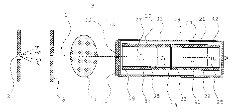
Fig. 1 illustrates schematically, in a cross sectional view, a
device for planar beam radiography, according to a first
embodiment of the present invention.
CA 02422614 2003-03-14
WO 02/25312 PCT/SE01/02018
4
Fig. 2 is a schematic top view of a first and a second anode,
respectively, as being comprised in the detector of Fig. 1.
Fig. 3 is a diagram showing the absorption coefficient of X-rays
due to absorption in tissue and bone, respectively, of human
body as a function of X-ray energy.
Fig. 4 is a schematic top view of a device having a plurality of
the detector of Fig. 1 in a stacked configuration.
Fig. 5 illustrates schematically, in a cross sectional view, a
device for planar beam radiography, according to a second
embodiment of the present invention.
Fig. 6 is a schematic cross sectional view of a detector
comprised in the device of Fig. 5, as being taken along line A-A
therein.
Fig. 7 illustrates schematically, in a cross sectional view, a
device for planar beam radiography, according to a third
embodiment of the present invention.
DETAILED DESCRIPTION OF PREFERRED EMBODIMENTS
In the following description, for purposes of explanation and
not limitation, specific details are set forth, such as
particular techniques and applications in order to provide a
thorough understanding of the present invention. However, it
will be apparent to one skilled in the art that the present
invention may be practiced in other embodiments that depart from
these specific details. In other instances, detailed
descriptions of well-known methods and apparatuses are omitted
so as not to obscure the description of the present invention
with unnecessary details.
Fig. 1 is a sectional view in a plane orthogonal to the plane of
a planar X-ray beam 1 of a device for planar beam radiography,
according to a first embodiment of the present invention. The
CA 02422614 2003-03-14
WO 02/25312 PCT/SE01/02018
device includes an X-ray source 3, which together with a first
thin collimator window 5 produces the planar fan-shaped X-ray
beam 1, for irradiation of an object 7 to be imaged.
The beam transmitted through the object 7 enters a detector 9.
5 Optionally a thin slit or second collimator window 11, which is
aligned with the X-ray beam, forms the entrance for the X-ray
beam 1 to the detector 9.
The detector 9 is oriented such that the X-ray photons can enter
sideways between a cathode 27 and an anode 19, between which a
space 13 capable of being filled with an ionizable gas or gas
mixture is arranged. A voltage U1 can be applied between cathode
17 and anode 19 for drift of electrons and ions in space 13
preferably in a direction substantially perpendicular to the
direction of the incident radiation. Cathode 17 and anode 19 are
preferably substantially parallel with each other.
The ionizable gas or gas mixture comprising for example 900
krypton and 10o carbon dioxide or for example 80% xenon and 20o
carbon dioxide. The gas may be under pressure, preferably in a
range 1-20 atm. Therefore, the detector includes a gas tight
housing 31 with a slit entrance window 33, through which the X-
ray beam 1 can enter the detector. In Fig. 1 the casing 31
encloses major parts of detector 9. It shall, however, be
appreciated that casing 31 may be arranged in other manners as
long as the space between the electrodes may be enclosed.
Further, a second cathode 21 and a second anode 23 are arranged
in detector 9, between which cathode 21 and anode 23 a solid
state wafer or slab 25 of an ionizable semiconducting material
is arranged. The second cathode 21, the second anode 23, and the
solid state wafer 25 are located within detector 9 such that
part of radiation 1 entered into space 13 through radiation
entrance 33 will propagate through space 13, and enter solid
state slab 25. The interaction of radiation 1 and the material
CA 02422614 2003-03-14
WO 02/25312 PCT/SE01/02018
6
of slab 25 will result in the creation of electrons and holes,
which may be drifted towards the anode 23 and cathode 21,
respectively, by means of a second voltage U~ applied between
cathode 21 and anode 23, preferably in a direction substantially
perpendicular to the direction of the incident radiation.
Cathode 2l and anode 23 are preferably arranged such that the
part of radiation beam 1, which enters solid state slab 25,
propagates between and substantially in parallel with cathode 21
and anode 23.
Alternatively, cathode 21 and anode 23 are arranged such that
part of radiation beam 1 can enter solid state slab 25 through
cathode 21 and substantially perpendicular to cathode 21 and
anode 23.
The solid state wafer 25 can be made of silicon but preferably
is of a higher Z semiconductor material. Preferably, the wafer
consists of high-resistivity CdZnTe, which can operate at room
temperature and can be fabricated into detectors, or other
semiconductor materials that have high-resistivity and that can
be fabricated into detectors. Of course, those skilled in the
art will recognize that virtually any semiconductor material may
be used in the invention.
Further aspects of the solid state section of detector 9, i.e.
of solid state wafer 25 and of cathode 21 and anode 23 are found
in U.S. 6,037,595 issued to Zingren, in U.S. 5,880,490 issued to
Antich et al. , and in references therein, said documents being
hereby incorporated by reference.
Furthermore, detector 9 comprises a read-out arrangement for
separate detection of the electrons drifted towards anode 19 and
23, respectively, as well as holes drifted towards the cathode
21. The read-out arrangement may be constituted of the anodes 19
and 23 themselves as in Fig. 1, or a separate read-out
arrangement may be arranged adjacent anodes 19 and 23, adjacent
CA 02422614 2003-03-14
WO 02/25312 PCT/SE01/02018
7
cathodes 17, 21, or elsewhere. Such detector 9 has thus a first
gas detector section and a second solid state detector section,
said sections being capable of separate detection of incident X-
rays.
The X-ray source 3, the first thin collimator window 5, the
optional collimator window 11 and the detector 9 are connected
and fixed in relation to each other by a suitable means for
example a frame or support (not shown in Fig. 1).
Referring now to Fig. 2, a possible configuration of anodes 19
and 23 (and thus configuration of the read-out arrangement) is
shown. Anode 19 is formed by an array of conductive read-out
strips 35 arranged electrically insulated from each other on a
dielectric layer or substrate 37, and anode 23 is formed by
another array of conductive read-out strips 39 arranged
electrically insulated from each other on another dielectric
layer 41. Similarly, the cathode 21 is formed by another array
of conductive read-out strips 49 arranged electrically insulated
from each other on another dielectric layer 42. Dielectric
layers 37 and 41 may alternatively be comprised of a single
dielectric layer. The strips may be formed by photolithographic
methods or electroforming, etc. The readout elements 39 and 49
can alternatively be situated on the semiconductor material 25
eliminating the need of substrates 41 and 42.
Strips 35 are placed side by side, strips 39 are placed side by
side, and strips 49 are placed side by side, wherein strips 35,
39 and 49 extend essentially in directions parallel to the
direction of incident X-ray photons of beam l, originating from
source 3, at each location. Thus, given a divergent beam l,
read-out strips 35, 39, and 49 are arranged in a fan-like
configuration and not parallelly as illustrated in Fig. 2. Such
fan-like configuration provides for an increased spatial
resolution and for compensation for parallax errors in any
detected images.
CA 02422614 2003-03-14
WO 02/25312 PCT/SE01/02018
8
The length and width of strips 35, 39 and 49 are adjusted to the
specific detector in order to obtain the desired (optimal)
spatial resolution.
Each of the strips 35, 39 and 49 is preferably connected to
processing electronics (not shown in Fig. 2) by means of a
respective separate signal conductor, whereby the signals from
each strip can be processed separately. As the read-out strips
35 and 39 also constitutes the anodes, the signal conductors
also connects the respective strip to the high voltage DC power
supply, with suitable couplings for separation.
Such design of the~read-out arrangement provides for capability
of separate detection of electrons derivable mainly from
ionization by transversely separated portions of planar
radiation beam 1 either by strips 35 or by strips 39. In such
manner one-dimensional imaging is enabled.
In the case the read-out arrangement is a separate arrangement,
anodes 35 and 39 can be formed as a unitary electrodes without
strips.
In an alternative configuration of anodes/read-out arrangement
(not illustrated), the strips are further divided into segments
in the direction of the incident X-rays, the segments being
electrically insulated from each other. Preferably a small
spacing extending perpendicular to the incident X-rays is
provided between each segment of respective strip. Each segment
is connected to the processing electronics by means of a
separate signal conductor, where the signals from each segment
preferably are processed separately. This read-out arrangement
can be used when further energy-resolved detection of the X-rays
is required.
Furthermore, the voltages U1 and U~ (i.e. the electrical fields
created thereby) can be kept high enough, during operation, to
CA 02422614 2003-03-14
WO 02/25312 PCT/SE01/02018
9
cause electron avalanche amplification within space 13 and
possibly but not necessarily in solid state slab 25.
Alternatively, other avalanche amplification arrangements or
field concentration means may be provided such that electrons
(and holes) freed in space 13 and possibly in solid state slab
25, respectively, can be amplified before detection.
Possible avalanche amplification arrangements for the gaseous
detector section are further described in our co-pending Swedish
patent application No. 9901325-2 entitled Radiation detector, an
apparatus for use in planar radiography and a method for
detecting ionizin g radiation and filed on April 14, 1999, which
application hereby is incorporated by reference. Possible
avalanche amplification arrangements for the solid state
detector section are further described in above said U.S.
patents, and in references therein.
In operation, the incident X-rays 1 enter the detector through
the optional thin slit or collimator window 11, if present, and
between cathode 17 and anode 19, preferably in a center plane
between them as indicated in Fig. 1. The incident X-rays 1 then
travel through the gas volume in a direction preferably
substantially parallel with electrodes 17 and 19 and get
absorbed, thus ionizing gas molecules in space 13. Some of the
X-rays 1 will pass through space 13, enter solid state slab 25
and ionize the ionizable semiconducting material therein.
Thus some X-ray are absorbed in region 27 in space 13 and some
X-rays may be absorbed in region 29 within the semiconductor 25.
X-rays absorbed in space 13 will cause electrons to be released,
which will drift towards anode 19 due to voltage U1 applied
between cathode 17 and anode 19. Correspondingly, X-rays
absorbed in solid state wafer 25 will cause electrons and holes
to be freed, which will drift towards anode 23 and cathode 21,
respectively, due to voltage U1 applied between cathode 21 and
CA 02422614 2003-03-14
WO 02/25312 PCT/SE01/02018
anode 23. If the voltages are kept high enough and/or if field
concentration means are provided (as discussed above) the freed
electrons are avalanche amplified during their travel towards
the anode. The electrons induce charges in the strips of the
5 read-out arrangement, i.e. in anode strips 35 and 39 in the
illustrated detector of Figs. 1 and 2, which are detected. If no
avalanche amplification takes place the major part of the signal
is due to collection of the liberated charges.
Each incident X-ray photon causes generally one induced pulse in
l0 one (or more) anode strip. The pulses are processed in the
processing electronics, which eventually shapes the pulses, and
integrates or counts the pulses from each strip representing one
picture element. The pulses can also be processed so as to
provide an energy measure for each pixel.
The depth within space 13 and/or solid state wafer 25 where an
interaction between an X-ray and the ionizable material takes
part is governed statistically by the absorption rate of the X-
rays in the material used. High-energy X-rays will generally
have a larger penetration depth than X-rays of lower energy.
As the X-rays enter the detector preferably in a direction
parallel to cathode plate 17 and anode plate 19, the detector
can easily be made with an interaction path long enough to allow
a major fraction of the incident X-ray photons to interact and
be detected.
Further, by means of designing the detector with thin inter-
electrode gaps, i.e. short distances between the cathode 17 and
the anode 19, and between the second cathode 21 and the second
anode 23, respectively, scattered radiation incident on the
detector (i.e. radiation traveling non-parallel with the
electrodes) will be geometrically 'discriminated to a great
extent (i.e. exiting the inter-electrode volumes without
becoming absorbed and thus affecting the position and energy
CA 02422614 2003-03-14
WO 02/25312 PCT/SE01/02018
11
resolutions adversely). It has been verified that much more than
990 of the scattered radiation can easily be discriminated.
Preferably, each inter-electrode distance is less, or much less,
than the length of the electrodes, i.e. dimension in the
direction of the incident radiation beam. Typically, the
distance is less than 2 mm, more preferably less than 1 mm, and
most preferably between 0.1 mm and 1 mm.
The detector in accordance with the present invention is
particularly useful when broadband X-ray radiation is used. In
such manner detector 9 may be adapted such that a substantial
portion of the lower energy radiation of the broadband radiation
is absorbed by the ionizable gas and a substantial portion of
the higher energy radiation of the broadband radiation is
absorbed by the io,nizable semiconducting material. In such
manner the detector provides for energy-resolved detection of
the radiation.
Interaction of broadband X-ray radiation with materia (e.g. the
gas in space 13) results in the release of photoelectrons of a
large range of kinetic energies. Electrons of higher kinetic
energies (up to 100 keV) are denoted long-range electrons and
will travel a relatively long path ( typically 1-20 mm at 1
atm.) before they become retarded and stopped (looses their
kinetic energy) in the materia, whereas electrons of lower
kinetic energy are denoted short-range electrons.
When the ionized materia relaxes, typically an Auger electron
and/or a fluorescent (X-ray) photon are released. An Auger
electron is a short-range electron with low kinetic energy
(typically 1-5 keV), which travel a relatively short path (0.01-
0.1 mm at 1 atm.) before it becomes stopped in the gas.
Therefore, during one single interaction of an X-ray photon with
a gas atom, e.g. Kr or Xe, several electrons will in many cases
be released simultaneously; both long-range and short-range
CA 02422614 2003-03-14
WO 02/25312 PCT/SE01/02018
12
electrons. Further, fluorescent photons may be emitted during
the interaction.
Both long-range and short-range electrons produce electron
tracks of secondary ionized electrons produced by the electrons
during the travel in the gas. When an electron has high kinetic
energy (e. g. 20-30 keV), the number of released electrons
(secondary ionized electrons) is low per path unit. For
electrons having low kinetic energy (typically 1-4 keV) the
number of released electrons (secondary ionized electrons) per
path unit is higher.
As the typical track length of a long-range electron is about 1-
mm at atmospheric pressure, such measure is a physical limit
of the spatial resolution. The fluorescent photons emitted can
also create ionization, as mentioned above. This ionization
15 takes place far away from the primary interaction with a typical
attenuation length of 1.5-250 mm at atmospheric pressure. This
ionization also deteriorates the spatial resolution and creates
background noise.
Consequently, the distance between cathode 17 and anode 19 is
20 preferably chosen such that detection of lower energy photons of
high spatial resolution is enabled. Thus, the distance shall
preferably be shorter than the attenuation length of the
fluorescent (X-ray) photons. This results in that a large number
of fluorescent photons will not cause ionization in space 13.
A further improvement of the spatial resolution is achieved if
the detector has a distance between cathode 17 and anode 19,
which is shorter than the length of the electron tracks (i.e.
the interaction length) of long-range electrons. This results in
that an even larger number of fluorescent photons and a large
number of long-range electrons will not undergo full energy loss
in the first space section.
CA 02422614 2003-03-14
WO 02/25312 PCT/SE01/02018
13
Still a further improvement of the spatial resolution is
achieved if the detector has a distance between cathode 17 and
anode 19, which is less than, or essentially equal to, a few
times the length of the electron tracks (i.e. interaction
length) of short-range electrons, e.g. 1-5 times the length of
the electron tracks of the short-range electrons. This results
in that a larger number of fluorescent photons and a larger
number of long-range electrons will not undergo full energy loss
in space 13. If the distance is smaller than the length of the
electron tracks of the short-range electrons, the efficiency
will go down since also short-range electrons will reach the
electrode plates before complete ionization.
By such geometrical discrimination of long-range electrons and
fluorescent photons a larger amount of the detected electrons
are caused by short-range electrons, which improves the spatial
resolution since the long-_range electrons and fluorescent
photons may cause release of electrons far from the interaction
position of the incident X-ray.
The distance between cathode 21 and anode 23 (i.e. the thickness
of solid state wafer 25) is preferably chosen such that
detection of higher energy photons is enabled. Thus, the
distance between cathode 21 and anode 23 shall preferably be
long enough to allow primary long-range electrons to be retarded
and to ionize the semiconducting material of the solid state
wafer, thus releasing shorter-range electrons. The efficiency of
detecting higher energy photons is thus improved to the cost of
a deteriorated spatial resolution.
Preferably though, the distance between cathode 21 and anode 23
is shorter than the attenuation length of fluorescent (X-ray)
photons. This results in that a great number of fluorescent
photons will not cause ionization in the semiconducting
material.
CA 02422614 2003-03-14
WO 02/25312 PCT/SE01/02018
14
A further improvement of the spatial resolution is achieved if
the detector has a distance between cathode 21 and anode 23,
which is essentially a few times the length of the electron
tracks (i.e. interaction length) of long-range electrons, e.g.
1-5 times the length of the electron tracks of the long-range
electrons.
Certainly, the distances between cathode 17 and anode 19 and
between cathode 21 and anode 23, respectively, the lengths of
space 13 and of solid state wafer 25 in a direction parallel
with the incident radiation, the composition of the gas mixture
in space 13, the pressure thereof, and the material of solid
state wafer 25, are designed for each particular application and
for each particular radiation spectrum used in order to achieve
desired detection efficiency, and required spatial and energy
resolution. However, thicknesses in the range of 0.1 - 5 mm, a
gas space length in the range of 10 - 200 mm, and a solid state
wafer length in the range of 0.1 - 10 mm may typically be
employed.
Further discussions of detector thicknesses and electrode gaps
are found in applicant's co-pending Swedish patent applications
No. 9901326-0 entitled A method for detecting ionizing
radiation, a radiation detector and an apparatus for use in
planar beam radiography and filed on April 14, 1999 and No.
0000388-9 entitled Detector and method for detection of ionizing
radiation and filed on February 08, 2000. These applications are
hereby incorporated by reference.
With reference now to Fig. 3 a particular application of the
present invention for measuring bone mineral density of humans
is to be described. Fig. 3 is a diagram showing the absorption
coefficient a of X-rays due to absorption in tissue, and in
bone, respectively, of human body as a function of X-ray energy.
In the diagram, the absorption coefficient varies from 1 to
roughly 0.4 as the X-ray photon energy varies from 0 to 150 keV.
CA 02422614 2003-03-14
WO 02/25312 PCT/SE01/02018
Shown is also the differential absorption coefficient (indicated
Tissue-Bone), which is an indication of the absorption
selectivity between tissue and bone, as a function of the photon
energy.
5 Normally the bone is surrounded by an unknown amount of tissue.
One commonly used method to estimate the amount of bone is to
detect transmitted X-rays at two different X-ray energies. One
exposure is made at X-ray energies where bone and tissue absorb
X-rays very differently; typically at 40 keV where the
10 differential absorption coefficient has a maximum, see Fig. 4.
Another exposure is made at energies where bone and tissue
absorb X-rays in a similar way; typically at energies above l00
keV, see Fig. 3 again. From these two measurements the amount of
bone is estimated. However, this requires that the detector is
15 capable of detecting low energy (around 40 keV) X-rays as well
as high energy X-rays (>100 keV), which is often a problem.
Furthermore, to obtain beams with a narrow energy distribution
at low energy, the incoming X-ray flux, which has a broad
spectrum, needs to be heavily filtered, putting a large load on
the X-ray tube. The two separate exposures, taken at different
times, also give rise to problems due to movements of the object
between the two exposures.
The present invention describes a combined gaseous-solid state
detector that can measure X-rays over a wide energy range. Low
~5 energy X-rays are preferably detected in the first gaseous
section of the detector due to their short absorption length.
High energy X-rays mainly traverse the first section of the
detector and are detected in the second solid state section. The
invention allows the same detector to be used to efficiently
detect X-rays at rather different energies with the same
detector, using the commonly used double exposure method.
Alternatively, the two measurements can be made simultaneously
using a broad X-ray spectrum of the incident X-rays. This second
CA 02422614 2003-03-14
WO 02/25312 PCT/SE01/02018
16
alternative requires less filtering of the X-rays and put less
load on the X-ray tube. Furthermore, by simultaneously detecting
the two energy intervals problems of movements between exposures
are reduced.
The device of Fig. 1 can be moved as a unit to scan an object,
which is to be examined. In 'a single detector system the
scanning can be done by a pivoting movement, rotating the unit
around an axis through for example the X-ray source 3 o.r the
detector 9. The location of the axis depends on the application
or use of the device, and possibly the axis can also run through
the object 7, in dome applications. It can also be done in a
translative movement where the detector and the collimator are
moved, or the object to be imaged is moved.
In a mufti-line configuration, where a number of detectors are
stacked, the scanning can be performed in various ways. In many
cases it can be advantageous if the device for radiography is
fixed and the object to be imaged is moved.
Fig. 4 shows schematically such a mufti-line configuration 91
according to an embodiment of the present invention having a
plurality of the inventive detectors 9 stacked, side-by-side of
each other. By this embodiment multiline scan can be achieved,
which reduces the overall scanning distance, as well as the
scanning time. The device of this embodiment includes an X-ray
source 3, which together with a number of collimator windows 5
produce a number of planar fan-shaped X-ray beams 1, for
irradiation of the object 7 to be imaged. The beams transmitted
through the object 7 optionally enter the individual stacked
detectors 9 through a number of second collimator windows 11,
which are aligned with the X-ray beams. The first collimator
windows 5 are arranged in a first rigid structure (not shown in
Fig. 7), and the optional second collimator windows 11 are
arranged in a second rigid structure (not shown in Fig. 7)
CA 02422614 2003-03-14
WO 02/25312 PCT/SE01/02018
17
attached to the detectors 9, or arranged separately on the
detectors.
The X-ray source 3, the first rigid structure, and the possible
second rigid structure including collimator windows 11,
respectively, and the stacked detectors 9, which are fixed to
each other, are connected and fixed in relation to each other by
a certain means, e.g. a frame or support (not shown in Fig. 4).
The so formed device for radiography can be moved as a unit to
scan an object, which is to be examined. In this multiline
configuration, the scanning can be done in a transverse
movement, perpendicular to the X-ray beam, as mentioned above.
It can also be advantageous if the device for radiography is
fixed and the object to be imaged is moved. Alternatively, the
collimator and the detector can be moved synchronously by a
commonly controlled motor.
A further advantage of using a stacked configuration, compared
to large two-dimensional detectors, is reduction of background
noise caused by X-ray photons scattered in the obj ect 7 . These
scattered X-ray photons travelling in directions not parallel to
the incident X-ray beam could cause "false" signals or
avalanches in one of the other detectors 9 in the stack, if
passing through anode and cathode plates and entering such a
space. This reduction is achieved by significant absorption of
(scattered) X-ray photons in the material of the anode and the
cathode plates, or the collimator 11. This background noise can
be further reduced by providing thin absorber plates (not
illustrated) between the stacked detectors. These absorber
plates or sheets can be made of a high atomic number material,
for example tungsten.
With reference now to Figs. 5 and 6, which illustrate
schematically, in cross sectional views, a device for planar
beam radiography and a detector 9' thereof, respectively, a
second illustrated embodiment of the present invention will be
CA 02422614 2003-03-14
WO 02/25312 PCT/SE01/02018
18
described. In Figs. 5 and 6 details and components, which are
identical with those of the Figs. 1 and 2 embodiment, have
identical reference numerals, and will not be further described.
The detector 9' comprises like detector 9 of Figs. 1 and 2 the
gaseous detector section including cathode 17, anode 19, and
space 13 capable of being filled with an ionizable gas.
However, instead of comprising a solid state detector section,
detector 9° comprises a scintillator based detector section 51
including a scintillating material 55 arranged such that part of
radiation beam 1 entered into space 13 through radiation
entrance 33 can ~ propagate through space 13 and enter
scintillating material 55, wherein the radiation is converted
into light therein. Further, scintillator section 51 comprises a
light detecting arrangement 53 for detection of the light
created. Preferably, scintillating material 55 is arranged in a
plurality of elongated scintillator elements aligned in an
array. Scintillator section 51 may further comprise
interstitial barriers 57 disposed between the scintillator
elements 55 so as to separate each scintillator element from
adjoining elements. Interstitial barriers 57 are comprised of a
material that absorbs the radiation entered into the
scintillating material, as well as scintillation light emitted
in the scintillator 55.
The plurality of elongated scintillator elements 55 are
arranged such that radiation beam 1 enters the plurality of
elongated scintillator elements 55 at a respective first end
thereof, whereas light detecting arrangement 53 is arranged at
a respective second end thereof. Preferably light emitted in
the scintillating material is detected in a direction parallel
with the incident radiation beam. However, detection may be
arranged at right angle thereto, or at virtually any angle
since the light is emitted istropically in the scintillating
material.
CA 02422614 2003-03-14
WO 02/25312 PCT/SE01/02018
19
If a planar radiation beam is entered into detector 9', each
detector section provides for one-dimensional imaging.
As in the previous embodiment, if radiation having a broadband
energy spectrum is entered into the detector, a substantial
portion of the lower energy radiation of the broadband radiation
is absorbed by the ionizable gas in space 13 and a substantial
portion of the higher energy radiation of the broadband
radiation is converted into light in scintillating material 55.
In such manner detector 9' provides for adapted energy-resolved
detection of the radiation.
Further, detector 9' may comprise amplifiers for amplifying the
electrons released in space 13 and the light emitted in the
scintillating material. Alternatively or additionally, any
other suitable amplification means may be provided.
With reference now to Fig. 7, which illustrates schematically,
in a cross sectional view, a device for planar beam
radiography, a third illustrated embodiment of the present
invention will be described. In Fig. 7 details and components,
which are identical with those of the previous embodiments, have
identical reference numerals, and will not be further described.
The Fig. 7 device comprises a detector 9" , which like detector
9 of Figs. 1 and 2 comprises the gaseous detector section
including cathode 17, anode 19, and space 13 capable of being
filled with an ionizable gas. Likewise, detector 9" comprises a
?5 second solid state section, however, this section being arranged
differently.
Further, this embodiment comprises a second X-ray source 3" , a
thin collimator window 5" for producing two planar fan-shaped
X-ray beams 1, 1" for irradiation of. an object 7 to be imaged.
The beams transmitted through the object 7 enter detector 9"
through entrance windows 33, 33" . Optionally a sheet 11"
CA 02422614 2003-03-14
WO 02/25312 PCT/SE01/02018
having two apertures aligned with the X-ray beams is arranged in
front of the entrance windows 33, 33" . The detector 9" is
oriented such that beam 1 enters the gaseous detector section,
i.e. into space 13 between cathode 17 and anode 19, and beam 1"
5 enters the second solid state detector section of detector 9" .
Space 13 is enclosed by casing 31" and entrance windows 33,
33" an is filled with an ionizable gas.
The second detector section can use the same cathode 17 as is
comprised in the gaseous detector section, but alternatively a
10 separate cathode (not illustrated) is provided. Further the
second detector section comprises an anode 19" substantially
in parallel with cathode 17, and a solid state slab 25" of an
ionizable semiconducting material arranged between cathode 17
and anode 19" . Solid state slab 25" is of a suitable material
15 and is ionized by radiation beam 1" . Further, a voltage UZ"
can be applied between cathode 17 and anode 19" for drifting
electrons created during ionization of the semiconducting
material towards anode 19" .
Anode 19" may be configured such as anode 19 of detector 9
20 (Figs. 1 and 2), i.e. with conductive read-out strips 39"
arranged electrically insulated from each other on a dielectric
layer or substrate 41" , to also constitute read-out
arrangement. The strips are preferably arranged side by side and
extend essentially in directions parallel to the direction of
incident X-ray photons of beam 1" . Alternatively, a separate
read-out arrangement (not illustrated) may be provided.
In both instances the read-out arrangement is arranged for
detection of electrons drifted towards anodes 19 and 23"
separately.
As in previous embodiments the gaseous detector section is
preferably adapted for detection of lower energy radiation
CA 02422614 2003-03-14
WO 02/25312 PCT/SE01/02018
21
whereas the solid state detector section is adapted for
detection of higher energy radiation.
Alternatively, instead of using two sources of radiation on
extended source of radiation may be used, which is divided into
two beams by mans of apertures or the like.
Yet alternatively, instead of using two radiation beams and
possibly simultaneous detection in the two detector sections,
the detector may be movable in a direction vertical to a single,
preferably broadband, radiation beam and the detector sections
with their respective entrance windows are, one after the other,
aligned with the radiation beam so as allow sequential detection
by the detector sections.
It shall further be appreciated that the detector may be
provided with suitable filters in front of the respective
detector section. Particularly, in such instance a filter, which
transmits only higher energy radiation, is arranged in front of
the solid state detector section and a filter, which transmits
only lower energy radiation, is arranged in front of the gaseous
detector section. The previous embodiments may provided such
filter in front of the solid state and the scintillator based
detector sections.
Further, yet another embodiment 'of the present invention (not
illustrated) uses the geometrical concept of the Fig. 7
embodiment, but comprises a scintillator based detector section
as a replacement for the solid state detector section.
It shall be appreciated that any of the above described
embodiments and alternatives may be combined in yet other
configurations.
It shall further be appreciated that the electrodes of the
detector sections in the various embodiments may be non-parallel
with each other. Preferably, respective cathode and anode are
CA 02422614 2003-03-14
WO 02/25312 PCT/SE01/02018
22
arranged with an angle a in respect to each other, whereby the
electrode ends facing the radiation source are located closer to
each other than the far ends thereof. In the case of a solid
state based detector section, the ionizable solid state wafer is
preferably then thinner in the end facing the radiation source.
In this respect further reference is made to our co-pending
Swedish patent application No. 9901324-5 entitled Radiation
detector and an apparatus for use in planar radiography and
filed on Aprile 14, 1999, which application hereby is
incorporated by reference.
Such variations ara not to be regarded as a departure from the
scope of the invention. All such modifications as would be
obvious to one skilled in the art are intended to be included
within the scope of the appended claims.