Note : Les descriptions sont présentées dans la langue officielle dans laquelle elles ont été soumises.
CA 02424017 2003-03-28
-1-
METHOD AND APPARATUS FOR REDUCING SWITCHING LOSSES IN A
SWITCHING CIRCUIT
BACKGROUND OF THE INVENTION
1. Field of Invention
This invention relates to switching circuits involving complementary switching
elements and more particularly to methods and apparatus for reducing
switching losses in such circuits.
2. Description of Related Art
Switching circuits involving complementary switching elements are commonly
found in power inverters, power supplies and Class D amplifiers. In these
applications, various types of switching elements may be employed. The
usual choices for switching elements include integrated Gate Bipolar
Transistors (IGBTs) and Metallic Oxide Semiconductor Field Effect
Transistors (MOSFETs).
MOSFETs have internal body diodes that result from their inherent design.
Tradeoffs are made when designing MOSFETs, to optimize and reduce static
and dynamic losses, but this often results in the creation of body diodes that
have poor inherent reverse recovery characteristics that contribute to losses
during reverse recovery of the devices. IGBTs have no internal body diode
and typically, external diodes are used with IGBTs to control reverse recovery
characteristics in a manner that reduces reverse recovery losses. IGBTs
however, exhibit greater static and dynamic losses.
Thus, designers of high frequency switching circuits are faced with selecting
between IGBTs and MOSFETS for use as switching elements and must make
such selections by making tradeoffs between reverse recovery losses and
static and dynamic losses, which can lead to an inefficient design.
CA 02424017 2003-03-28
-2-
SUMMARY OF THE INVENTION
The present invention addresses the above problem by providing a method of
reducing switching losses in a leg of a switching circuit during commutation
of
cun-ent between first and second complementary switching elements thereof.
The method involves impeding changes in current flow between a load current
node and a first supply conductor through a first path comprised of a first
saturable inductor and the first switching element, while impeding changes in
current flow between the load current node and a second supply conductor
through a second path comprised of a second saturable inductor and the
second switching element.
The method may involve pre-saturating the first saturable inductor with
current in
a direction from the load current node to the first supply conductor so that
the
first saturable inductor is saturated when the first switching element is shut
off.
Pre-saturating may involve operating the first switching element in an on
condition in which sufficient current is flowing therethrough to saturate the
first
saturable inductor.
Impeding changes in current flow may involve passing current through a series
combination of the first saturable inductor and a body diode of the first
switching
element.
Impeding changes in current flow through the first path may involve operating
the first saturable inductor in a saturated mode while operating the second
saturable inductor in a linear mode.
Operating the second saturable inductor in a linear mode may involve switching
the second switching element on while the second saturable inductor impedes
instantaneous current flow therethrough such that at the instant the second
switching element is turned on the instantaneous current therethrough is zero.
CA 02424017 2003-03-28
-3-
Operating the first saturable inductor in a saturated mode while operating the
second saturable inductor in a linear mode may be followed by operating the
first saturable inductor in a linear mode while operating the second saturable
inductor in a saturated mode.
The first saturable inductor may impede reverse recovery current flow from the
first supply conductor to the load current node thereby limiting a
contribution to
total current flow in the second path.
The method may involve resetting current flow to zero through the second
saturable inductor prior to commutating current from the first switching
element
to the second switching element. Resetting current flow to zero may involve
switching the second switching element off and passing current through the
second saturable inductor to a clamping diode connected to the first supply
conductor. Resetting may also involve turning the first switching element on
while passing current through the clamping diode to rob current from the
clamping diode to reduce a voltage drop thereacross to a voltage below a turn
on voltage thereof to shut the diode off.
In accordance with another aspect of the invention, there is provided a
switching
circuit apparatus comprising a load current node operable to receive load
current, a first current path comprised of a first saturable inductor
connected to
the load current node and a first switching element connected to the first
saturable inductor and a first supply conductor. The apparatus further
includes a
second current path comprised of a second saturable inductor connected to the
load current node and a second switching element connected to the second
saturable inductor and a second supply conductor. The first saturable inductor
is
operable to impede changes in current flow between the load current node and
the first supply conductor while the second saturable inductor is operable to
impede changes in current flow between the toad current node and the second
supply conductor.
CA 02424017 2003-03-28
The first saturable inductor may be configured to be pre-saturated with
current in
a direction from the load current node to the first supply conductor so that
the
first saturable inductor is saturated when the first switching element is shut
off.
The apparatus may further include a reset circuit for resetting current flow
to
zero through the second saturable inductor prior to commutation of current
from
the first switching element to the second switching element.
The reset circuit may include a diode connected to the second saturable
inductor and the first supply conductor.
The first and second saturable inductors may be configured such that the first
saturable inductor is operated in a saturated mode while the second saturable
inductor is operated in a linear mode at an instant when the second switching
element is turned on.
The first and second saturable inductors may be configured such that operating
the first saturable inductor in a saturated mode while operating the second
saturable inductor in a linear mode is followed by operating the first
saturable
inductor in a linear mode while operating the second saturable inductor in a
saturated mode.
Other aspects and features of the present invention will become apparent to
those ordinarily skilled in the art upon review of the following description
of
specific embodiments of the invention in conjunction with the accompanying
figures.
BRIEF DESCRIPTION OF THE DRAWINGS
In drawings which illustrate embodiments of the invention,
CA 02424017 2003-03-28
-5-
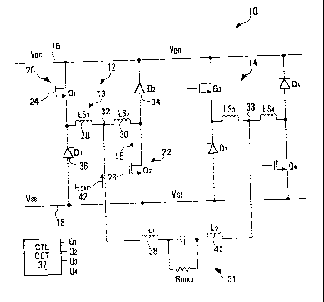
Figure 1 is a schematic diagram of a switching circuit having first and
second legs, according to a first embodiment of the invention;
Figure 2 is a schematic representation of a simplified equivalent circuit for
the first leg in a condition where a first switching element Q1
thereof is turned on and is in a steady state, at an instant in time
immediately before commutation of current from Q1 to a second
switching element Q2;
Figure 3 is a schematic representation of an equivalent circuit representing
the operation of the first leg during the onset of reverse recovery in
Q1 immediately after Q1 is turned off after being in the steady
state condition depicted in Figure 2;
Figure 4 is a schematic representation of an equivalent circuit representing
the operation of the first leg immediately after Q2 is turned on
wherein a first saturable inductor of the leg is saturated while a
second saturable inductor of the leg is in a linear mode;
Figure 5 is a schematic representation of an equivalent circuit representing
the operation of the leg after Q2 is turned on and in a condition
where the first saturabie inductor is in a linear mode and the
second saturable inductor is in a saturated mode; and
Figure 6 is a schematic representation of an equivalent circuit representing
a reset operation on the second saturable inductor.
DETAILED DESCRIPTION
Referring to Figure 1 a switching circuit according to a first embodiment of
the
invention is shown generally at 10. In this embodiment, the switching circuit
10 is a high frequency inverter switching circuit having first and second legs
CA 02424017 2003-03-28
-6-
shown generally at 12 and 14, each of which may be considered a separate
switching circuit for the purposes of this description.
The first leg 12 has a load current node 32 operable to receive load current
from a load inductor 38 in a load circuit 31 that is being supplied with power
from the switching circuit 10. The first leg 12 also has a first current path
13
comprised of a first saturable inductor 28 connected to the load current node
32 and a first switching element (Q1 ) 20 connected to the first saturable
inductor 28 and a first supply conductor (Vdd) 16. The first leg 12 also has a
second current path 15 comprised of a second saturable inductor 30
connected to the load current node 32 and, in this mode, a second switching
element (Q2) 22 connected to the second saturable inductor 30 and a second
supply conductor (Vss) 18. The first supply conductor 16 may be at a
potential of, say, 250 Vdc relative to the second supply conductor 18, for
example.
The first saturable inductor 28 is operable to impede changes in current flow
between the load current node 32 and the first supply conductor 16 while the
second saturable inductor 30 is operable to impede changes in current flow
between the load current node 32 and the second supply conductor 18.
A first clamping diode (D1 ) 36 is connected between the second supply
conductor 18 and a first node connecting together the first switching element
Q1 and the first saturable inductor 28 and a second clamping diode (D2) 34 is
connected between the first supply conductor 16 and a second node
connecting together the second switching element Q2 and the second
saturable inductor 30.
The second leg 14 is similar to the first leg 12 and has a second load current
node 33, third and fourth switching elements Q3 and Q4 similar to switching
elements Q1 and Q2, diodes D3 and D4 similar to diodes D1 and D2 and
CA 02424017 2003-03-28
-7-
saturable inductors LS3 and LS4 similar to the first and second saturable
inductors LS1 and LS2, all connected in a manner similar to corresponding
components of the first leg.
A control circuit 37 is in communication with the switching elements Q1-Q4
and produces switching control signals that control the switching elements to
place them in on or off states. The control signals are produced such that Q1
and Q2 are never on at the same time and such that Q3 and Q4 are never on
at the same time. More particularly, the control signals are produced such
that the switching elements sequence through four states in which the
switching elements are on or off. For example, if a 1 is used to represent a
switching element being on and a 0 is used to represent a switching element
being off, each state may be represented by a binary number, the digits of
which represent respective on or off conditions of respective switching
elements Q1, Q2, Q3 and Q4. A first state may thus be represented by the
number 1010, a second state by the number 0110, a third state by the number
0101 and a fourth state by the number 1001. The two most significant digits
of each number represent the states of the first and second switching
elements Q1 and Q2 and the two least significant digits represent the states
of the third and fourth switching elements Q3 and Q4. The first and third
states (1010 and 0101 ) are generally regarded as passive states and the
second and fourth states (0110 and 1001 ) are regarded as active states.
The switching circuit 10 may be part of a 3kW power supply, for example, in
which case each switching element may effectively receive a switching signal
having frequency of 30kHz, and each switching element may each be a
Fairchild Semiconductor FQA55N25 manufactured by Fairchild
Semiconductor of California, USA, or similar, for example and the diodes may
each be an Advanced Power Technology (APT) APT30D40B, or similar.
Each of the first and second saturable inductors 28 and 30 may be comprised
of a 0.5 in. by 0.25 in torroidal ferrite core such as Siemens B64290-K004-
CA 02424017 2003-03-28
.$_
X830 on which is wound 6 turns of 24 gauge, 7 strand single insulated twisted
wire, for example.
Focussing on the first leg 12 of the switching circuit 10, comprising the
first
and second switching elements Q1 and Q2, the present invention reduces
switching losses that can otherwise occur when the switching elements
change from a passive state (Q1 and Q3 on; Q2 and Q4 off) to an active state
(Q1 and Q4 on; Q2 and Q3 off).
Operation
Each leg 12 and 14 of the switching circuit 10 is identical and therefore only
the first leg 12 will be described here. Only the transition from the first
passive state (1010) to the first active state (0110) will be described here,
in
connection with commutation of current from the first switching element Q1 to
the second switching element Q2. It will be appreciated that a similar
description would apply to the transition between the second passive state
and the second active state in respect of commutation from the second
switching element Q2 to the first switching element Q1 and that corresponding
analogies are applicable to the third and fourth switching elements Q3 and C~4
for corresponding commutations of current in these switching elements.
The commutation of current from the first switching element Q1 to the second
switching element Q2 in the first leg 12 may be better understood with
reference to Figures 2, 3, 4, and 5, which show various equivalent circuits
for
the first leg 12 at progressive instants in time during commutation.
Q1 on: Stead s
Figure 2 depicts a simplified equivalent circuit for the first leg 12 in a
condition
where Q1 is turned on and is in a steady state, at an instant in time
immediately before commutation. Referring back to Figure 1, during
commutation, relatively large load inductors 38 and 40 of the load circuit 35
CA 02424017 2003-03-28
_g_
act as a constant current source such that current flow into and out of the
load
current node 32 may be regarded as constant. Current flow into the load
current node 32 is from the load inductor 38 and current flow out of the load
current node is through the first current path 13 comprised of the first
saturable inductor 28 and the drain-source resistance rds~~n)1 of Q1 to the
first supply conductor 16. The first saturable inductor 28 is configured to
have
suitable inductance and core saturation properties to ensure that with
sufficient load current flow therethrough it will saturate when the first
switching
element Q1 is on and current therethrough has reached a steady state.
Referring to Figure 2, the first saturable inductor 28 is saturated and the
current is steady at this instant and thus the first safiurable inductor 28
presents virtually no impedance to current flow out of the load current node
32. Virtually all impedance to current flow out of the load current node 32 is
provided by rds~on)1. Referring back to Figure 1, the second clamping diode
34 is not turned on, because the voltage thereacross is less than the junction
voltage thereof because rds~on)1 is so small. While the first saturable
inductor 28 is saturated, the control circuit 37 may issue a control signal to
shut off the first switching element Q1. The first saturable inductor 28 is
thus
pre-saturated with current in a direction from the load current node 32 to the
first supply conductor 16 at the instant the first switching element Q1 is
shut
off. At this instant the control circuit 37 maintains the state of a control
signal
maintaining the second switching element Q2 in an off state for a very short
period of time After Q1 is shut off to ensure that both Q1 and Q2 are not on
at
the same time.
CA 02424017 2003-03-28
-10-
Q1 off: onset of reverse recovery immediately after steady state
Figure 3 depicts an equivalent circuit representing the operation of the first
leg
12 during the onset of reverse recovery in Q1 immediately after Q1 is turned
off after being in the steady state condition depicted in Figure 2.
Referring to Figure 3, at the instant Q1 is turned off, it no longer acts like
a
resistor (i.e., rds~on)1 ), but rather like a diode due to its inherent body
diode
44. Thus, load current continues to flow into the load current node 32 from
the load and flows out of the load current node 32 through the series
combination of the first saturable inductor 28 and the body diode 44 of Q1 to
the first supply conductor 16. Referring to Figure 1, at this time, the
control
circuit 37 issues a signal to the second switching element Q2 to cause it to
turn on.
Q1 off, Q2 on: continuation of reverse recovery of Q1. onset of current into
Q2
Referring to Figure 4, at the instant Q2 is turned on, it provides a second
path
for current flow out of the load current node 32. The second saturable
inductor
30 impedes changes in current through this second current path 15 and the
internal resistance rds~on)2 of Q2 provides virtually all of the DC resistance
to
current flow therethrough.
rds(on)2 ~s ~pically very low, so a very high current could potentially flow
through Q2 were it not for the second saturable inductor 30. This very high
current would be supplied by the load inductor 38 and by a reverse current
operable to flow in a reverse direction 46 through the body diode 44 of Q1 due
to the presence of minority carriers in a junction of the body diode that
determine a reverse recovery time thereof. However, the rate of change of
current flow through Q2 is limited by the second saturable inductor 30.
CA 02424017 2003-03-28
-11-
In a MOSFET reverse recovery time is dependent upon its reverse breakdown
voltage, the potential across the MOSFET and the current flowing through the
MOSFET at the time it is switched off. An approximation for reverse recovery
time as a function of inductance in a circuit having a MOSFET is provided by
authors Ned Mohan, Tore Underland, and William Robbins in a text entitled
Power Electronics: Converters Applications and Design published by John
Wiley and Sons, New York, NY 1989. This approximation is set forth below:
(4) t,.,. = 2.8 x 10⁻⁶ BV~, Iinv Ls
~dd ~ss
where trr = reverse recovery time
BV~ = reverse breakdown voltage of MOSFET
linv = Inverter (toad) current
LS = inductance of one of LS., and LSZ (same)
V~, = Positive pole supply voltage
VSS = Negative pole supply voltage
In addition, the above mentioned text provides an approximation of reverse
recovery current as follows:
(5) hr = 2.8 x 10⁻⁶ BYE line{V~ - TT
Ls
CA 02424017 2003-03-28
-12-
The undesirable effects of switching losses include increased heat dissipation
and electromagnetic noise. Both of these factors are mitigated by reducing
the reverse recovery current, however, as can be seen from the above
equations, reduction of the reverse recovery current requires a larger
inductor
to increase the time constant of the circuit to provide more time for the
minority carriers in the body diode 44 to recombine. This, however; limits the
operable duty cycle of the switching elements and reductions in duty cycle
reduce the ability to deliver a significant output voltage. Thus, the
selection of
the first and second saturable inductors 28 and 30 must be made such that
reverse recovery current is minimized, while duty cycle is maximized. Within
these limits, suitable properties for the first and second saturable inductors
28
and 30 can be determined as at least a first approximation and then
measurements can be taken on a prototype to tune the values of the inductors
to values that provide optimum efficiency of the leg.
Still referring to Figure 4, it will be appreciated that at the instant Q2 is
turned
on, no current is flowing through rds~on)2 since the second saturable inductor
30 is not saturated and effectively blocks instantaneous current flow.
Consequently, Q2 experiences a zero current transition when it is turned on.
Since the current supplied by the load inductor (38) is constant, the reverse
recovery current that would have been able to flow into the load current node
32 to contribute to the potentially high current through Q2 is limited by the
second saturable inductor 30. The second saturable inductor 30 thus reduces
reverse recovery current and reduces power losses in the first leg 12.
The current flow through rds~o~)2 and the second saturable inductor 30
increases at a rate determined by the second saturable inductor while it is in
a
linear mode or unsaturated mode of operation. Effectively, the impedance to
CA 02424017 2003-03-28
-13-
current flow through Q2 changes from infinite to rdston)2 and as this
impedance decreases, current flowing from the load current node 32 through
the first body diode 44 to the first supply conductor 16 is robbed by current
increasingly favoring the second current path 15 through the second saturable
inductor 30 and Q2. As the current through the second saturable inductor 30
increases, current flow through the body diode 44 decreases, until the current
through the body diode drops to a certain value, at which the first saturable
inductor 28 is no longer saturated and enters a linear mode of operation.
While the first saturable inductor 28 is in the linear mode it impedes changes
in current flow between the load current node 32 and the first supply
conductor 16. The first and second saturable inductors 28 and 30 are
matched such that by the time the first saturable inductor enters the linear
mode of operation, the second saturable inductor is saturated. The equivalent
circuit for this condition is shown in Figure 5.
Referring to Figure 5, when the second saturable inductor 30 becomes
saturated, current can change very quickly in the second path 15 but the first
saturable inductor 28 limits the rate of change of current through Q1 and thus
takes over in limiting the rate of robbing current from Q1 to Q2 until the
body
diode 44 of Q1 has recovered and is effectively shut off due to the reverse
bias thereon as a result of the potential between the first supply conductor
16
and the second supply conductor 18. Any reverse current that would flow in
the reverse direction through the body diode 44 of the first switching element
Q1 is impeded by the first saturable inductor 28 which limits the contribution
to
total current flow in the second current path 15 comprised of the second
saturable inductor 30 and the second switching element Q2.
Thus, as shown in Figure 4, at the instant Q2 is turned on, initially the
first
saturable inductor 28 is saturated and the second saturable inductor 30 is in
a
linear mode and thus the first saturable inductor presents little opposition
to
CA 02424017 2003-03-28
-14-
current flow, while the second saturable inductor primarily limits current
flow
into Q2 and hence limits reverse current and switching losses in Q1. This
also provides for zero current switching of Q2.
As shown in Figure 5, as current through Q2 increases, the first saturable
inductor 28 becomes unsaturated at about the same time the second
saturable inductor 30 becomes saturated and, at this time, the first saturable
inductor 28 primarily limits reverse current flow in Q1 and hence limits
current
flow from the first supply conductor (Vdd) into Q2. Thus, operating the first
saturable inductor 28 in the saturated mode while operating the second
saturable inductor 30 in a linear mode is followed by operating the first
saturable inductor 28 in a linear mode while operating the second saturable
inductor 30 in a saturated mode. The first saturable inductor 28 impedes
current flow between the load current node 32 and the first supply conductor
16 when it is operating in its linear mode and the second saturable inductor
30
impedes current flow between the load current node and the second supply
conductor 18 when it is operating in its linear mode.
Referring back to Figure 1, when current is flowing into the load current node
32 as shown, and current is to be commutated from Q2 to Q1, the control
circuit 37 issues a signal to Q2 to shut Q2 off while Q1 is still off, before
turning Q1 on again. Thus Q1 and Q2 are both off for a brief period of time
before Q1 is turned on again. An equivalent circuit of the leg 12 for the
brief
instant in time when both Q1 and Q2 are off after Q2 has been on, is shown in
Figure 6.
At the instant Q2 is shut off and before Q1 is switched on, current that was
flowing through the second saturable inductor 30 now flows through the
second clamping diode 34 and the second saturable inductor remains
saturated and presents virtually no impedance to current through the diode.
At the same time, current begins to flow from the load current node 32
CA 02424017 2003-03-28
-15-
through the first saturable inductor 28 and through the body diode 44 of the
first switching element Q1, but this current flow is impeded by the first
saturable inductor 28.
When Q1 is switched on, it presents an alternate path for current from the
load current node 32 with an impedance provided by rds~on)1 and the first
saturable inductor 28. The resistance rds~on)1 is considerably less than the
on resistance of the second clamping diode 34 and thus, current flow shifts
from the second current path 15, now comprised of the second saturable
inductor 30 and the second clamping diode 34 to the first current path 13
comprised of the first saturable inductor 28 and Q1. This shift in current
flow
is initially impeded by the first saturable inductor 28 because the second
saturable inductor 30 is still saturated. At about the time the second
saturable
inductor 30 desaturates and enters its linear mode, the first saturable
inductor
28 becomes saturated and thus any further impedance to the shift in current is
provided by the second saturable inductor. During this shift in current, since
the ultimate voltage drop across rds~on)1 will be much less than the forward
voltage of the. second clamping diode 34, when the voltage drop across the
second saturable inductor 30 drops to a certain value, the second clamping
diode 34 shuts off and no further current flows through the second current
path 15. Thus, current flow through fhe second saturable inductor 30 is reset
to zero by switching the second switching element Q2 off and passing current
through the second saturable inductor 30 to the second clamping diode 34
connected to the first supply conductor 16 and then turning on the first
switching element Q1 to rob current through the second clamping diode 34 to
reduce a voltage drop across the second clamping diode to a voltage below a
turn on voltage thereof to shut the diode off: The voltage across the second
saturable inductor 30 at the point where the second clamping diode 34 shuts
CA 02424017 2003-03-28
-16-
off may be referred to as the reset voltage of the second saturable inductor
30
and may be given by the equation:
VReset = VD - rds~o~)1 ~ LOAD
Where VReset - the reset voltage for the second saturable
inductor
Vp - forward voltage of the second clamping diode
(34)
rds~on~l - on resistance of Q1
(LOAD - current through second saturable inductor
In effect, the second clamping diode 34 acts as a reset circuit for resetting
current flow to zero through the second saturable inductor 30 prior to
commutation of current from the first switching element Q1 to the second
switching element Q2.
The effect of the switching circuit topology described herein is to limit
reverse
recovery current in both Q1 and Q2, thereby reducing switching losses while
at the same time providing zero current switching for Q1 and Q2. This
increases the efficiency of the leg 12 and reduces stresses on Q1 and Q2,
thereby extending their lives.
While specific embodiments of the invention have been described and
illustrated, such embodiments should be considered illustrative of the
invention only and not as limiting the invention as construed in accordance
with the accompanying claims.