Note : Les descriptions sont présentées dans la langue officielle dans laquelle elles ont été soumises.
CA 02424639 2003-04-07
10019340
1
AN INTERMESH MEMORY DEVICE
TECHNICAL FIELD
This invention relates to a memory device, and in particular, to an
intermesh memory device.
BACKGROUND
Conventional read-only memory (ROM) circuits are implemented as
special-purpose integrated circuits for the permanent storage of program
instructions and electronic data. For example, a ROM circuit can be
manufactured with specific instructions for the operation of a computer
system.
Typically, a ROM circuit consists of an array of memory cells on a
semiconductor, and each memory cell has a transistor that is fabricated to
indicate a logic "one" or a logic "zero" based on how the semiconductor is
implanted to create the transistor. The data is permanently stored with a
memory cell, and it cannot then be erased or altered electrically. Each of the
transistors can be formed so as to have one of the two predetermined logic
values.
A programmable ROM (PROM) circuit is designed with memory cells
having programmable memory components that can be programmed after the
semiconductor chip has been manufactured. The memory cells of a PROM
device are programmed with data (e.g., a logic one or a logic zero) when the
data is burned into the chip. This is accomplished by forming contacts that
define the threshold voltage levels near the end of the manufacturing process,
or after the manufacturing process. When a PROM device is programmed,
CA 02424639 2003-04-07
10019340
2
the device can be irnplemenied like a conventional ROM chip in that the data
cannot be electrically altered.
Due to the costs of fabricating semiconductor memory devices, and the
design of smaller integrated circuit-based electronic devices, there is an
ever-present need to provide non-volatile memory circuits that take up less
space, have improved memory storage capacity, and are inexpensive to
manufacture.
SUMMARY
An intermesh memory device includes.memory components that each
have a determinable resistance value and electronic switches that each
control current through one or more of the memory components such that a
potential is applied to the memory components. A first electronic switch of
the
intermesh memory device is electrically coupled to an input of a memory
component and a second electronic switch is electrically coupled to an output
of the memory component. The first electronic switch and the second
electronic switch are configured together to apply a potential to the memory
component.
BRIEF DESCRIPTION OF THE DRAWINGS
The same numbers are used throughout the drawings to reference like
features and components.
Fig. 1 illustrates an embodiment of a memory component electrically
coupled to electronic switches, and exemplary memory components.
Fig. 2 illustrates an embodiment of a schematic section of a memory
array formed with an exemplary memory component and electronic switches
shown in Fig. 1.
Fig. 3 illustrates an embodiment of a memory array formed with an
embodiment of an exemplary memory component and electronic switches
shown in Fig. 1.
CA 02424639 2003-04-07
10019340
3
Fig. 4 illustrates an embodiment of an intermesh memory array formed
with an embodiment of an exemplary memory component and electronic
switches shown in Fig. 1.
Fig. 5 illustrates an embodiment of an intermesh memory array shown
as a schematic section in a vertical perspective.
Fig. 6 illustrates an embodiment of an intermesh memory array shown
as a schematic section in a vertical perspective.
Fig. 7 illustrates an exemplary schematic diagram of the intermesh
memory array shown in Fig. 4 where the intermesh memory array is formed
with an embodiment of an exemplary memory component and electronic
switches shown in Fig. 1.
Fig. 8 illustrates an exemplary schematic diagram of an intermesh
memory array formed with an embodiment of exemplary memory components
electrically coupled to electronic switches.
Fig. 9 is block diagram that illustrates various components of an
exemplary computing device that can be utilized to implement an embodiment
of an intermesh memory device.
Fig. 10 is a flow diagram that describes an exemplary method for
making and utilizing an intermesh memory device.
DETAILED DESCRIPTION
The following describes an intermesh memory array that includes write-
once memory components which can be implemented in a memory device for
fast read and write access. The intermesh memory array architecture is much
faster than conventional memory devices and can be implemented as a
programmable read-only memory device for a digital memory application,
such as a compact flash memory for a digital camera for example. Further,
the memory devices can be less expensive to manufacture and can be
smaller, yet have more memory capacity than conventional memory devices.
Less expensive and smaller memory devices provide greater design flexibility
for integrated circuit-based electronic devices.
CA 02424639 2003-04-07
10019340
4
!n an implementation, an intermesh memory device is configured with a
first array of memory components and a second array of memory
components. The memory components That form the first memory array
intersect, overlap, andlor are substantially perpendicular to the memory
components that form the second memory array. For example, memory
components that form the first memory array are formed in rows in an
x-dimension and the memory components that form the second memory array
are formed in columns in a y-dimension, such that the memory components in
the two memory arrays intersect perpendicularly.
The memory components that form the first and second memory arrays
are coupled to pillars which are conductive vias in the intermesh memory
device that alternate between drive and sense and are activated with
complementary logic levels. The memory components are electrically coupled
between each adjacent drive and sense pillar. The intermesh memory device
architecture provides that two adjacent rows of pillars can be driven and all
of
the columns sensed, or two adjacent columns of pillars driven and all of the
rows sensed.
General reference is made herein to various examples of memory
devices. Although specific examples may refer to memory devices having
particular memory component implementations, such examples are not meant
to limit the scope of the claims or the description, but are meant to provide
a
specific understanding of the data storage techniques described herein.
Furthermore, !t is to be appreciated that the described memory components
are exemplary, and are not intended to limit application of the data storage
techniques. Accordingly, other memory devices having components different
from and/or in addition to those described herein can be used to implement
the described intermesh memory device.
Exemplan,~lntermesh Memory Devices
Fig. 1 illustrates an exemplary memory circuit 100 that includes an
embodiment of a memory component 1102 electrically coupled to electronic
switches 104 and 106. Electronic switch 104 is implemented as an n-channel
field effect transistor (FET) that is electrically coupled to memory component
CA 02424639 2003-04-07
10019340
102. The transistor 104 has a high voltage 108 applied to turn the transistor
on such that current flows through the transistor. Electronic switch 106 is
implemented as a p-channel FET that is also electrically coupled to memory
component 102. The transistor 106 has a low voltage 110 applied to turn the
transistor on such that current flows through the transistor. Those skilled in
the art will recognize that "high" and "low" voltages as described herein are
relative to each other such that a high voltage, such as high voltage 108, is
implemented at transistor operational levels and is a relatively higher
voltage
than low voltage 110. Conversely, a low voltage is a relatively lower voltage
than a high voltage.
When both of the transistors 104 and 106 are turned on with the
applied high voltage 108 and low voltage 110, respectively, a potential is
applied to memory component 102. The potential is derived from a positive
drive voltage 112 (+V) at an input, or drive node 114, of memory component
102 and from a sense voltage 116 (+VA) at an output, or sense node 118, of
memory component 102. A sense amplifier 120 senses the resistance value
of memory component 102. The sense amplifier 120 can be implemented
with sense amplifiers that include a differential, analog, or digital sense
amplifier.
Memory component 102 can be implemented with any type of
electrically resistive material, such as an oxide, in an integrated circuit
and/or
as a resistive memory component, such as with a resistor. Those skilled in
the art will recognize that many different combinations of materials and
designs are available to fabricate memory devices and the memory
components. Exemplary memory components 122 and 124 can be
implemented as memory component 102 in memory circuit 100. Memory
component 122 is implemented with a resistor 126 connected in series with a
control element 128. Memory component 124 is implemented with an anti-
fuse device 130 connected in series with a diode 132. Further, a memory
component can be implemented with an anti-fuse device connected in series
with a control element.
CA 02424639 2003-04-07
10019340
6
A control element, such as control element 128 in memory component
122, functions to allow the selection of a particular memory component in an
array of memory components forming a memory device. The control element
128 can be implemented with a linear or nonlinear resistor, a tunnel junction
diode, a tunnel diode, an anti-fuse device, or a Schottky, PN, or PIN
semiconductor diode.
An anti-fuse device, such as anti-fuse device 130 in memory
component 124, is a tunnel-junction, one-time programmable device. The
tunnel-junction of an anti-fuse device is a thin oxide junction that electrons
"tunnel" through when a pre-determined, relatively high potential is applied
across the anti-fuse device. The applied potential causes an electrical
connection when the oxide junction is destroyed creating a short having a low
resistance value. Anti-fuse device 130 can be implemented with any number
of available components and types of fuses or anti-fuses, such as a
LeComber, Silicide, Tunnel Junction, Oxide Rupture, or any other similar fuse
components. Further, anti-fuse device 130 can be implemented with any
number of re-writeable data storage elements.
Fig. 2 illustrates a schematic section of an embodiment of a memory
array 200 formed with rows 202 of memory components and transistor
electronic switches similar to those shown in Fig. 1. For illustrative
purposes,
the memory components, such as memory component 204, are each shown
as an anti-fuse device connected in series with a control element.
Alternatively, the memory components can be implemented with any
combination of resistive memory devices and control elements as described
with reference to memory component 102 (Fig. 1).
Further, the memory components in memory array 200 (and other
memory component examples described herein) can be implemented with
any re-writeable data storage elements as well as any programmable,
write-once memory components, such as the exemplary memory component
124 implemented with an anti-fuse device 130 in series with a diode 132 as
shown in Fig. 1. Alternatively, the memory components can be implemented
CA 02424639 2003-04-07
10019340
7
with one of many different combinations of materials and designs that are
available to fabricate memory cells for memory devices.
In memory array 200, the electronic switches are implemented as
alternating n-channel FETs and p-channel FETs that are each electrically
coupled to one or more of the memory components. For example, transistor
206 is electrically coupled to memory component 204 and to memory
component 208 at a node, or connection point 210. Similarly, transistor 212 is
electrically coupled to memory components 214 and 216 at a node, or
connection point 218.
In memory array 200, two adjacent rows 202(2) and 202(3) of
transistors are driven high, while the remaining rows of transistors in memory
array 200 have a tow voltage applied. In row 202(2), a p-channel FET 220
has a high voltage 222 applied to turn the transistor off while the n-channel
FET 206 is turned on when high voltage 222 is applied. Similarly, in row
202(3), the n-channel FET 212 has a high voltage 224 applied to turn the
transistor on while a p-channel FET 226 is turned off when high voltage 224 is
applied.
In row 202(1), an n-channel FET 228 has a low voltage 230 applied to
turn the transistor off while a p-channel FET 232 is turned on when low
voltage 230 is applied. Similarly, In row 202(4), a p-channel FET 234 has a
low voltage 236 applied to turn the transistor on while an n-channel FET 238
is turned off when low voltage 236 is applied. Those skilled in the art will
recognize that the applied transistor high and low voltages are relative to
each
other such that a high voltage, such as high voltages 222 and 224, are
implemented at transistor operational levels and are a higher voltage than low
voltages 230 andlor 236. Further, any two adjacent rows in a memory array
can be driven high while the remaining rows in the memory array are driven
low, or remain low. Additionally, the circuit logic can be inverted such that
any
two adjacent rows of alternating n-channel FETs and p-channel FETs are
driven low while the remaining rows in the memory array are driven high.
When any two adjacent rows of transistors are driven high, such as the
transistors in rows 202(2) and 202(3), a potential is applied to a single
CA 02424639 2003-04-07
10019340
8
memory component in each column 240 of memory array 200 such that a
resistance value of a memory component in a column can be determined. for
example, when both of the transistors 212 and 234 in column 240(1 ) are
turned on with the applied high voltage 224 and low voltage 236, respectively,
a potential is applied to memory component 216. The potential is derived
from a positive drive voltage 242 (+V) at. an input, or drive node 218, of
memory component 216 and from a sense voltage 244 (+VA) at an output, or
sense node 246, of memory component 216. A current path 248 is created
through transistor 212, memory component 216, and transistor 234.
Similarly, when both of the transistors 206 and 232 in column 240(2)
are turned on with the applied high valtage 222 and low voltage 230,
respectively, a potential is applied io memory component 204. The potential
is derived from a positive drive voltage 250 (+V) at an input, or drive node
210, of memory component 204 and from a sense voltage 252 (+VA) at an
output, or sense node 254, of memory cornponent 204. A current path 256 is
created through transistor 206, memory component 204, and transistor 232.
A sense amplifier 258 senses the resistance value of memory component
204. The sense amplifier 258 can be implemented with sense amplifiers that
include a differential, analog, or digital sense amplifier.
Fig. 3 illustrates a section of an embodiment of a memory array 300
formed with rows of memory components 302 and transistor electronic
switches as shown in Figs. 1 and 2. Fig. 3 further illustrates that when any
two adjacent rows of transistors are driven high, such as in rows 304(2) and
304(3), a potential is applied to a memory component in each column 306 of
memory array 300 such that a resistance value of a memory component in
any column can be determined. One or more sense amplifiers 308 sense the
resistance value of a memory component in a selected column 306.
For example, when row 304(2) is driven high, every other transistor in
the row is turned on to apply a drive voltage to a memory component in every
other corresponding column. As described above, the transistors are
implemented as alternating n-channel FETs and p-channel FETs that are
turned on and/or off with high and low voltages applied. Row 304(1) is driven
CA 02424639 2003-04-07
10019340
9
low such that every other transistor in each column corresponding to the
transistors that are turned on in row 304(2) are also turned on to apply a
sense voltage to the memory components. Thus, the resistance value of
memory component 310 in column 306(1), memory component 312 in column
306(3), and memory component 314 in column 306(5) can all be determined
at the same time.
Similarly, when row 304(3) is driven high, every other transistor in the
row is turned on to apply a drive voltage to a memory component in every
other corresponding column 306(2), 306(4), and 306(6). Row 304(4) is driven
low such that every other transistor in each column corresponding the
transistors that are turned on in row 304(3) are also turned on to apply a
sense voltage to the memory components. Thus, the resistance value of
memory component 316 in column 306(2), memory component 318 in column
306(4), and memory component 320 in column 306(6) can all be determined
at the same time, along with memory components 310, 312, and 314.
Fig. 4 illustrates a section of an embodiment of an intermesh memory
array 400 that is formed with rows of memory components (1.e., memory array
300 shown in Fig. 3) and additional columns of memory components 402.
Intermesh memory array 400 is also implemented with transistor electronic
switches as shown in Figs. 1 and 2. Fig. 4 shows that memory components
402 can be added to memory array 300 to form the intermesh memory array
400 in which either rows andlor columns of the memory components can be
sensed at any one time.
Fig. 4 illustrates that when any two adjacent columns of transistors are
driven high, such as in columns 404(2) and 404(3), a potential is applied to a
memory component in each row 406 of memory array 400 such that a
resistance value of a memory component in any row can be determined. One
or more sense amplifiers 408 sense the resistance value of a memory
component in a selected row 406.
For example, when column 404(2) is driven high, every other transistor
in the column is turned on to apply a drive voltage to a memory component in
every other corresponding row. As described above, the transistors are
CA 02424639 2003-04-07
90019340
implemented as alternating n-channel FETs and p-channel FETs that are
turned on andlor ofif with high and low voltages applied. Column 404(1) is
driven Iew such that every other transistor in each row corresponding to the
transistors that are turned on in column 404(2) are also turned on to apply a
sense voltage to the memory components.. Thus, the resistance value of
memory component 410 in row 406(1), memory component 412 in row
406(3), and memory component 414 in row 406(5) can all be determined at
the same time.
Similarly, when column 404(3) is driven high, every other transistor in
the column is turned on to apply a drive voltage to a memory component in
every other corresponding raw 406(2), 406(4), and 406(6). Column 404(4) is
driven low such that every other transistor in each row corresponding the
transistors that are turned on in column 404(3) are also turned on to apply a
sense voltage to the memory components. Thus, the resistance value of
memory component 416 in row 406(2), memory component 418 in row
406(4), and memory component 420 in row 406(6) can all be determined at
the same time, along with memory components 410, 412, and 414.
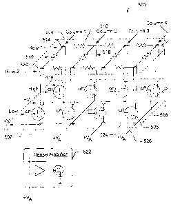
Fig. 5 illustrates an embodiment of an intermesh memory array 500
shown as a schematic section in a vertical perspective. Intermesh memory
array 500 has a semiconductor region 502 and a device region 504. The
semiconductor region 502 includes electronic switches, such as an n-channel
FET 506 and a p-channel FET 508, which are fabricated in semiconductive
material on a semiconductor substrate with any fabrication andlor
manufacturing process known to those skilled in the art. Device region 504
includes electrically resistive components, such as resistive memory
components 510 and 512, that are fabricated in the device region which is
offset from the semiconductive material.
Intermesh memory array 500 also includes electrically conductive vias,
such as conductive via 514, which electrically couples an electronic switch
(e.g., a transistor) to one or more of the electrically resistive components.
For
example, electrically conductive via 514 couples a transistor 516 to resistive
memory components 510 and 512. Memory component 510 is electrically
CA 02424639 2003-04-07
1G01~340
11
coupled to both conductive vias 514 and 518. Similarly, memory component
512 is electrically coupled to both conductive vias 514 and 520. The
conductive vias can be fabricated with electrically conductive material such
as
copper or aluminum, or with alloys or doped silicon.
It is to be appreciated that the connection nodes, such as the input
drive node 1 i4 and output sense node 118 of memory component 102
(Fig. 1 ), the drive node 218 and sense node 246 of memory component 216
(Fig.2), the drive node 270 and sense node 254 of memory component 204
(Fig.2), and the drive and sense nodes illustrated in Figs. 3 and 4 can be
implemented as electrically conductive vias to offset the memory components
from the transistor region of a memory device incorporating the memory
arrays described herein.
Although the resistive memory components are illustrated as resistors
in Fig. 5, the memory components can be implemented with any combination
of resistive memory devices and control elements as described with reference
to memory component 102 (Fig. 1). Further, the memory components in
intermesh memory array 500 can be implemented with any re-writeable data
storage elements as well as any programmable, write-once memory
components, such as the exemplary memory component 204 implemented
with an anti-fuse device connected in series with a control element (Fig. 2).
To simplify the description, Fig. 5 shows only a few memory components and
associated transistors. Those skilled in the art will appreciate that
intermesh
memory array 500 can be fabricated with any number of memory
components, transistors, and other drive and sense circuitry, such as sense
amplifier 522, as part of a memory device.
In practice, intermesh memory array 500 can be fabricated as a
semiconductor memory device with any fabrication and/or manufacturing
process known to those skilled in the art. Further, the voltage control lines,
such as positive drive voltage line 524 (+V) and sense voltage line 526 (+VA),
can be fabricated above semiconductor region 502 in device region 504 which
includes the electrically resistive components. Forming the voltage control
lines and the memory components offset from the semiconductor substrate
CA 02424639 2003-04-07
1001340
12
conserves space on the semiconductor substrate so that intermesh memory
array 500 is a smaller memory device that provides greater design flexibility
and density for integrated circuit-based electronic devices.
The term "semiconductor substrate", as used herein, includes
semiconductive material and is not limited to bulk semiconductive material,
such as a silicon wafer, either alone or in assemblies comprising other
materials thereon, and semiconductive material layers, either alone or in
assemblies comprising other materials. T'he term "substrate" refers to any
supporting structure including but not limited to a semiconductor substrate
which can be made of silicon, glass, gallium arsenide, silicon on sapphire
(SOS), epitaxial formations, germanium, germanium silicon, diamond, silicon
on insulator (SO/) material, selective implantation of oxygen (SIMOX)
substrates, and/or like substrate materials. A substrate may also be made of
plastic.
Fig. 6 illustrates an embodiment of an intermesh memory array 600
shown as a schematic section in a vertical perspective, and as a variation of
the intermesh memory array 500 shown in Fig. 5. Intermesh memory array
600 also has a semiconductor region 602 and a device region 604. The
device region 604 includes a first memory array 606 that includes the
resistive
memory components in rows 608, such as memory component 610 in row
608(1) and memory component 612 in row 608(2). The device region also
includes a second memory array 614 that includes the resistive memory
components in columns 616, such as memory component 618 in column
616(1) and memory component 620 in column 616(4).
The first memory array 606 is offset 622 from the second memory array
614. Those skilled in the art will recognize that memory arrays 606 and 614
can be fabricated together or independently with any known semiconductor
fabrication andlor manufacturing process. Further, the first set of memory
components in rows 608 that form the first memory array 608 intersect,
overlap, andlor are substantially perpendicular to the second set of memory
components in columns 616 which form the second memory array 614.
Those skilled in the art will recognize that although the sets of memory
CA 02424639 2003-04-07
10019340
13
components are described and illustrated as perpendicular, or substantially
perpendicular, in practice the memory components can be implemented in any
one of many positions and configurations, to include memory components that
are perpendicular on a horizontal plane, both vertical and horizontal on two
planes, perpendicular on a vertical plane, and the like.
The semiconductor region 602 includes transistors, such as an
n-channel FET 624 and a p-channel FET 626, which are fabricated in
semiconductive material on a semiconductor substrate with any fabrication
andlor manufacturing process known to those skilled in the art. Intermesh
memory array 600 also includes electrically conductive vias, such as
conductive via 628, which electrically couples a transistor to one or more of
the resistive memory components. For example, electrically conductive via
628 couples a transistor 630 to resistive memory components 632 and 618.
Memory component 632 is electrically coupled to both conductive vias 628
and 634. Similarly, memory component 618 is electrically coupled to both
conductive vias 628 and 636.
Although the resistive memory components are illustrated as resistors
in Fig. 6, the memory components can be implemented with any combination
of resistive memory devices and control elements as described with reference
to memory component 102 (Fig. 1 ). Further, the memory components in
intermesh memory array 600 can be implemented with any re-writeabie data
storage elements as well as any programmable, write-once memory
components, such as the exemplary memory component 204 implemented
with an anti-fuse device connected in series with a control element (Fig. 2).
To simplify the description, Fig. 6 shows only a few memory components and
associated transistors. Those skilled in the art will appreciate that
intermesh
memory array 600 can be fabricated with any number of memory
components, transistors, and other drive and sense circuitry, such as sense
amplifier 638, as part of a memory device,
In practice, intermesh memory array 600 can be fabricated as a
semiconductor memory device with any fabrication andlor manufacturing
process known to those skilled in the art. Further, the voltage control fines,
CA 02424639 2003-04-07
10019340
14
such as positive drive voltage line 640 (+V) and sense voltage line 642 (+VA),
can be fabricated above semiconductor region 602 in device region 604 which
includes the electrically resistive components.
Fig. 7 illustrates an exemplary schematic diagram of an embodiment of
an intermesh memory array 700 similar 'lo intermesh memory array 400
(Fig. 4) which is formed with rows and colurnns of memory components, such
as memory components 702 and 704. The memory array 700 can be
fabricated to include an embodiment of an exemplary memory component and
the electronic switches shown in Fig. 1. Further, intermesh memory array 700
can be implemented as either of the exemplary intermesh memory arrays 500
(Fig. 5) and 600 (Fig. 6), where a device region that includes electrically
resistive components is offset from a semiconductor region that includes
electronic switches, such as the alternating n-channel and p-channel FETs.
Intermesh memory array 7G0 is implemented with transistor electronic
switches such that either rows 706 or columns 708 of the memory
components can be sensed at any one time. The memory components are
arranged in rows 706 extending along an x-direction 710 and in columns 708
extending along a y-direction 712. Only a few memory components are
shown to simplify the description, such as memory component 702 in row
706(1) and memory component 704 in column 708(1). In practice, memory
array 700 can be implemented as a ROM (read-only memory) device having
multiple memory components, as a programmable memory device having
re-writeable data storage elements, or as a logic device, such as a one-time
programmable gate array. The functionality of such a gate array would be
similar to that of a field programmable gate array (FPGA) which is an
integrated circuit that can be programmed after manufacture.
Additionally, the rows 706 of memory components and the columns 708
of memory components do not have to be fabricated perpendicular to each
other as illustrated in Fig. 7. Those skilled in the art will recognize the
various
fabrication techniques and semiconductor design layouts that can be
implemented to fabricate intermesh memory array 700.
CA 02424639 2003-04-07
100193p0
The resistance value of any one memory component in the intermesh
memory array 700 can be designed to be relatively high (e.g. 10Meg ohms),
which translates to a logic bit value of one, or relatively low (e.g. 100K
ohms),
which translates to a logic bit value of zero. Correlating a relatively high
resistance memory component with a Ic>gic one, and a relatively low
resistance memory component with a logic zero is an implementation design
choice. Accordingly, a relatively high resistance memory component can be
defined as a logic zero and a relatively low resistance memory component can
be defined as a logic one.
The resistance value of a selected memory component is determinable
and can be sensed by applying a voltage potential to a memory component
and measuring the current that flows through the memory component. The
resistance value is proportional to the sense current. During a read operation
to determine the resistance value of a memory component, a decoder (not
shown) selects two adjacent rows of transistors, or two adjacent columns of
transistors, to apply a positive drive voltage 714. A second decoder (not
shown) selects one or more columns 708 of memory components, or one or
more rows 706 of memory components, to be connected to a sense amplifier
716 that senses the resistance value of a selected memory component in the
intermesh memory array 700. The sense amplifier 716 can be implemented
with sense amplifiers that include a differential, analog, or digital sense
amplifier.
Each memory component in the intermesh memory array 700, such as
memory component 702 in row 706(1) and memory component 704 in column
708(1), can be fabricated with an anti-fuse device that indicates a high
resistance value when a relatively low voltage is applied across the anti-fuse
device to read a particular memory component. A selected memory
component can be programmed by applying a relatively high potential across
the anti-fuse device to fuse the tunnel-junction in the device. When an anti-
fuse device is programmed, it will indicate a low resistance when a relatively
low voltage is applied across the particular memory component. The anti-fuse
devices can be utilized as programmable switches that allow the intermesh
CA 02424639 2003-04-07
10019340
16
memory array to be implemented as a programmable logic device. The
anti-fuse devices can be utilized as both logic elements and as routing
interconnects. Unlike traditional switching elements, the anti-fuse devices
can
be optimized to have a very low resistance once programmed which allows for
high-speed interconnects and lower power levels.
Fig. 7 illustrates that when any two adjacent rows of transistors are
driven high, such as in rows 706(2) and 706(3), a potential is applied to a
memory component in each column 708 of the intermesh memory array 700
such that a resistance value of a memory component in any column can be
determined. One or more sense amplifiers 716 sense the resistance value of
a memory component in a selected column 708.
For example, when the transistors in row 706(2) are driven high, every
other transistor in the row is turned on to apply a drive voltage to a memory
component in every other corresponding column. As described above, the
transistors are implemented as alternating n-channel FETs and p-channel
FETs that are turned on and/or off with high and low voltages applied. Row
706(1) is driven low such that every other transistor in each column
corresponding to the transistors that are turned on in row 706(2) are also
turned on to apply a sense voltage to the memory components. Thus, the
resistance value of memory component 718 in column 708(2) can be
determined.
An example implementation of intermesh memory array 700 would
include a sixty-four column andlor sixty-four row intermesh memory array
implemented with one sense amplifier for every eight rows and/or columns
(i.e., eight sense amplifiers). Thus, when two adjacent rows of transistors
are
driven high, the sense amplifiers can be utilized to read an eight-bit word at
one time. The eight-bit word would be comprised of the logic state
corresponding to the resistance value of a memory component in columns
one, nine, seventeen, etc. up to column fifty-seven. A next eight-bit word
would be comprised of the logic state corresponding to the resistance value of
a memory component in columns two, ten, eighteen, etc. up to column fifty-
eight, and so on.
CA 02424639 2003-04-07
10019340
17
Fig. 8 illustrates an embodiment of an intermesh memory array 800
formed with exemplary memory components, such as memory components
802 and 804. The memory components can be fabricated as an embodiment
of an exemplary memory component 122, 124, or 204 as shown in Figs. 1
and 2. Additionally, each memory component in intermesh memory array 800
can be fabricated with an anti-fuse device that indicates a high resistance
value when a relatively low voltage is applied across the anti-fuse device to
read a particular memory component.
A selected memory component can be programmed by applying a
relatively high potential across the anti-fuse device to fuse the tunnel-
junction
in the device. When an anti-fuse device is programmed, it will indicate a low
resistance when a relatively low voltage is applied across the particular
memory component. The anti-fuse devices can be utilized as programmable
switches that allow the intermesh memory array to be implemented as a
programmable logic device.
Intermesh memory array includes alternating rows 806 of drive and
sense connection nodes, and alternating columns 808 of drive and sense
connection nodes. The rows 806 of drive and sense connection nodes are
arranged in rows extending along an x-direction 810 and the columns 808 of
drive and sense connection nodes are arranged in columns extending along a
y-direction 812. As described above with reference to intem~esh memory
array 500 (Fig. 5), the drive and sense connection nodes can be implemented
as electrically conductive vias (also referred to as "pillars") to offset the
memory components from a transistor region of a memory device
incorporating the intermesh memory array 800.
Intermesh memory array 800 is implemented with two transistor
electronic switches per row and per column of the connection nodes such that
the memory components electrically coupled to the transistors in either rows
806 or columns 808 can be sensed at any one time. The transistor electronic
switches are implemented as n-channel FETs and as p-channel FETs.
The memory components are each electrically coupled to a drive
connection node and to a sense connection node. For example, memory
CA 02424639 2003-04-07
10019340
18
component 802 is electrically coupled to drive connection node 814 at row
806(3) and column 808(3), and coupled to sense connection node 816 at row
806(4) and column 808(4). Similarly, memory component 804 is electrically
coupled to drive connection node 818 at row 806(3) and column 808(5), and
to sense connection node 820 at row 806(2) and column 808(6).
Only a few memory components and connection nodes are shown to
simplify the description. In practice, intermesh memory array 800 can be
implemented as a ROM (read-only memory) device having multiple memory
components, or as a logic device, such as a one-time programmable gate
array. The functionality of such a gate array would be similar to that of a
field
programmable gate array (FPGA) which is an integrated circuit that can be
programmed after manufacture. Additionally, the memory components, such
as memory components 802 and 804, and the rows 806 and columns 808 of
connection nodes do not have to be fabricated perpendicular to each other as
illustrated in Fig. 8. Those skilled in the art will recognize the various
fabrication techniques and semiconductor design layouts that can be
implemented to fabricate intermesh memory array 800.
The resistance value of a selected memory component is determinable
and can be sensed by applying a voltage potential to a memory component
and measuring the current that flows through the memory component. The
resistance value is proportional to the sense current. During a read operation
to determine the resistance value of a rnemory component, a decoder (not
shown) selects two drive transistors 822 and 824 to apply a positive drive
voltage (+V) 826 to every other drive connection node in either the rows or
columns. As illustrated in Fig. 7, every other drive connection node, such as
drive connection node 814, has the positive drive voltage applied.
A second decoder (not shown) selects two sense transistors 828 and
830 to apply a sense voltage (+VA) 832 to every other sense connection node
in either the rows or columns. As illustrated, every other sense connection
node, such as sense connection node 816, has the sense voltage applied.
One or more of the memory components electrically coupled to the transistors
in either rows 806 or columns 808 can t>e connected to a sense amplifier 834
CA 02424639 2003-04-07
10019340
19
that senses the resistance value of a selected memory component in the
intermesh memory array 800.
Fig. 8 illustrates that when any two drive transistors are driven high,
such as p-channel FET 822 and n-channel FET 824, and when two sense
transistors are driven high, such as p-channel FET 828 and n-channel FET
830, a potential is applied to memory component 802. Sense amplifier 834
senses the resistance value of memory component 802. Alternatively, the
circuit logic can be inverted such that any two drive transistors are driven
low
in combination with two corresponding sense transistors driven low to apply a
potential to a memory component.
Exemplary Intermesh Memopr Device Application Environment
Fig. 9 illustrates various components of an exemplary computing
device 900 that can be utilized to implement an embodiment of an intermesh
memory device as described herein. Computing device 900 is only one
memory device application environment, and those skilled in the art will
recognize that any number of computing type devices having a memory
device can be utilized to implement the data storage techniques. For
example, computing type devices include multifunction devices which, as the
name implies, is a device for multiple functions which are related to, but not
limited to, printing, copying, scanning, to include image acquisition and text
recognition, sending and receiving faxes, print media handling, andlor data
communication, either by print media or electronic media, such as email ar
electronic fax.
Further, computing type devices include, but are not limited to,
personal computers, server computers, client devices, microprocessor-based
systems, set top boxes, programmable consumer electronics, network PCs,
minicomputers, and hand-held portable devices such as a personal digital
assistant (PDA), a portable computing device, and similar mobile computing
devices.
Computing device 900 includes one or more processors 902,
input/output interfaces 904 for the input and/or output of data, and user
input
devices 906. Processors) 902 process various instructions to control the
CA 02424639 2003-04-07
10019340
operation of computing device 900, while inpuUoutput interfaces 904 provide a
mechanism for computing device 900 to communicate with other electronic
and computing devices. User input devices 906 can include a keyboard,
mouse, pointing device, and/or other mechanisms to interact with, and to input
information to computing device 900.
Inputloutput interfaces 904 can include serial, parallel, andlor network
interfaces. A network interface allows devices coupled to a common data
communication network to communicate information with computing device
900. Similarly, a communication interface, such as a serial and/or parallel
interface, a USB interface, an Ethernet interface, and/or any combination of
similar communication interfaces provides a data communication path directly
between computing device 900 and another electronic or computing device.
Computing device 900 also includes a memory device 908 (such as
ROM andlor MRAM device), a disk drive 910, a floppy disk drive 912, and a
CD-ROM andlor DVD drive 914, all of which provide data storage
mechanisms for computing device 900. Memory device 908 can be
implemented with any one of the memory devices 100 (Fig. 1), 200 (Fig. 2),
and 300 (Fig. 3). Those skilled in the art will recognize that any number and
combination of memory and storage devices can be connected with, or
implemented within, computing device 900. Although not shown, a system
bus typically connects the various components within computing device 900.
Computing device 900 also includes application components 916 and
can include an integrated display device 918, such as for a multifunction
device display on a device control panel, or for a personal digital assistant
(PDA), a portable computing device, and similar mobile computing devices.
Application components 916 provide a runtime environment in which software
applications or components can run or execute on processors) 902. Further,
an application component 916 can be implemented as a data storage
application to perform the data storage techniques described herein.
For a multifunction implementation of computing device 900, such as
for a device that prints, copies, scans, and the like, device 900 can include
a
print unit that selectively applies an imaging medium such as liquid ink or
CA 02424639 2003-04-07
10019340
21
toner to a print media in accordance with print data corresponding to a print
job. Further, device 900 can include a scan unit that can be implemented as
an optical scanner to produce machine-readable image data signals that are
representative of a scanned image, such as a photograph or a page of printed
text. The image data signals produced by scan unit can be used to reproduce
the scanned image on a display device or with a printing device.
Methods for Data Storage with an Intermesh Memory Device
Fig. 10 illustrates a method 1000 for implementing data storage with an
intermesh memory device. The order in which the method is described is not
intended to be construed as a (imitation, and any number of the described
method blocks can be combined in any order to implement the method for
data storage. Furthermore, the method can be implemented in any suitable
hardware, software, firmware, or combination thereof.
At block 1002, electronic switches are formed on a semiconductor
substrate. The electronic switches can be formed with voltage controlled
switches, such as field effect transistors. For example, intermesh memory
arrays 500, 600, and 700 (Figs.5, 6, and 7, respectively) can include
alternating p-channel FETs and n-channel FETs formed on a semiconductor
substrate. Further, intermesh memory array 800 (Fig. 8) can include
p-channel FETs andlor n-channel FETs formed on a semiconductor substrate.
At block 1004, electrically conductive vias are formed. For example,
conductive via 514 is formed to electrically couple electronic switch 516
(e.g.,
a transistor) to resistive memory components 510 and 512 (Fig. 5).
At block 1006, an intermesh array of memory components are formed.
For example, device region 504 of intermesh memory array 500 includes
electrically resistive components, such as resistive memory components 510
and 512, that are fabricated in the device region which is offset from the
semiconductive material in the semiconductor region 502 (Fig. 5). Memory
component 510 is electrically coupled to transistors, such as transistor 516,
with conductive vias 514 and 518. Similarly, memory component 512 is
electrically coupled to transistors, such as transistor 516, with conductive
vias
514 and 520. Further, intermesh memory array 600 includes a first memory
CA 02424639 2003-04-07
10019340
22
array 606 that is offset from a second mernory array 614. The first set of
memory components that form the first memory array 606 intersect, overlap,
and/or are substantially perpendicular to the second set of memory
components which form the second memory array 614.
At block 1008, the resistance value of individual memory components
is programmed by applying a voltage to the individual memory components.
For example, the resistance value of an anti-fuse device implemented as a
memory component can be configured by applying a potential to the write-
once device. Further, the resistance value of the memory components in an
intermesh memory array can be configured by exposing an individual memory
component to light and/or to a heat source.
At block 1010, a resistance value of a memory component is
determined when a potential is applied to the memory component. For
example, when both of the transistors 206 and 232 in column 240(2) are
turned on with the applied high voltage 222 and low voltage 230, respectively,
a potential is applied to memory component 204 (Fig. 2). The potential is
derived from a positive drive voltage 250 (+V) at an input, or drive node 210,
of memory component 204 and from a sense voltage 252 (+VA) at an output,
or sense node 254, of memory component 204. A current path 256 is created
through transistor 206, memory component 204, and transistor 232. The
sense amplifier 258 senses the resistance value of memory component 204.
At block 1012, the determined resistance value of a memory
component is associated with a logic state of a data bit. For example, an
application component 916 of computing device 900, or another electronic
device implementing an intermesh memory array described herein, can read
the resistance value of memory components and derive a bit sequence that
represents any form of electronic data, such as computer-executable
instructions.
Fig. 11 illustrates a method 1050 for implementing data storage with an
intermesh memory device. The order in which the method is described is not
intended to be construed as a limitation, and any number of the described
method blocks can be combined in any order to implement the method for
CA 02424639 2003-04-07
16019340
23
data storage. Furthermore, the method can be implemented in any suitable
hardware, software, firmware, or combination thereof.
At block 1052, a first electronic switch coupled to one or more drive
pillars is turned on. For example, transistor 206 coupled to drive pillar 210
is
turned on when high voltage 222 is applied to the transistors in row 202(2)
(Fig. 2).
At block 1054, a first voltage is applied to an input of a first memory
component with a first drive pillar which is coupled to the input of the first
memory component. For example, drive voltage 250 (+V) is applied to the
input of memory component 204 with drive pillar 210.
At block 1056, the first voltage is applied to an input of a second
memory component with a second drive pillar which is coupled to the input of
the second memory component. For example, drive voltage 714 (+V) is
applied to the input of two memory components coupled to two respective
drive pillars (D) in row 706(2) (Fig. 7). Further, drive voltage 826 (+V) is
applied to the input of a first memory component 802 with drive pillar 814 in
row 806(3), and the drive voltage 826 is also applied to the input of a second
memory component with a drive pillar in row 806(7) (Fig. 8).
At block 1058, a second electronic switch coupled to one or more
sense pillars is turned on. For example, transistor 232 coupled to sense
pillar
254 is turned on when low voltage 230 is applied to the transistors in row
202(1) (Fig. 2).
At block 1060, a second voltage is applied to an output of the first
memory component with a first sense pillar which is coupled to the output of
the first memory component. For example, sense voltage 252 (+VA) is applied
to the output of memory component 204 with sense pillar 254 (Fig. 2).
At block 1062, the second voltage is applied to an output of the second
memory component with a second sense pillar which is coupled to the output
of the second memory component. For example, sense voltage +VA is
applied to the output of two memory components coupled to two respective
sense pillars (S) in columns 708(2) and 708(N) (Fig. 7). Further, sense
CA 02424639 2003-04-07
1GG19340
24
voltage 832 (+VA) is applied to the output of a first memory component 802
with sense pillar 816 in row 806(4) (Fig. 8).
At block 1064, the resistance value of the first and second memory
components is sensed. For example, memory components 310 and 312 in
columns 306(1) and 306(3), respectively, are sensed with one or more sense
amplifiers 308 (Fig. 3). Similarly, memory components 416 and 418 in rows
406(2) and 406(4), respectively, are sensed with one or more sense amplifiers
408 (Fig. 4).
Conclusion
Although the invention has been described in language specific to
structural features and/or methods, it is to be understood that the invention
defined in the appended claims is not necessarily limited to the specific
features or methods described. Rather, the specific features and methods are
disclosed as preferred forms of implementing the claimed invention.