Note : Les descriptions sont présentées dans la langue officielle dans laquelle elles ont été soumises.
CA 02427867 2003-05-05
WO 02/40095 PCT/CA00/01374
BODY ELECTRONIC IMPhANT AND ARTIFICIAh VISION SYSTEM THEREOF
FIELD OF THE INVENTION
The present invention relates to body electronic
implants, and more particularly to a body electronic implant
that can be used to stimulate the visual cortex of a blind
person for providing artificial vision, or to stimulate other
body organs or tissues or nerves for other purposes, and that
can also be used as a monitoring instrument for diagnostic
purposes.
BACKGROUND
Blindness is still nowadays difficult to cure.
Technologies such as speech synthesisers, 3D tactile displays
and dedicated scanners improve the quality of life of blind
persons by allowing them to read text and manipulate money.
However, for seeing., the situation is still the same as a
hundred, or even a thousand years ago.
Since electrical stimulation techniques are applied in
many circumstances to enhance or restore organ function, a
few research teams are working on the recuperation of a
limited but functional vision to totally blind persons. A
functional vision means that the person will be able to do,
without assistance, most of the tasks being part of every day
life. It will be limited since no system in the near future
will be able to replace the natural vision system with the
same accuracy. The required resolution and data processing
capabilities are simply too large.
A person is considered legally blind if a visual
dysfunction is present and sufficient to greatly affect his
everyday life. The medical criterions vary from one country
to another but, in general, those who are considered legally
blind include a specific group of totally blind persons. This
1
CA 02427867 2003-05-05
WO 02/40095 PCT/CA00/01374
means that they do not see anything and live in a world of
complete darkness. The causes of blindness are numerous. Some
causes originate in the eye and others are related to the
visual pathways.
The history of human visual stimulation began in 1960
when it was found that when a specific part of the human
brain was stimulated with an electrical current, a fixed
light spot appeared in the visual field of the patient . The
part of the brain was later identified as the visual cortex
and the light spots are called phasphenes. In 1968, results
of clinical experiments. related to visual stimulation were
first published. The experiments were done with different
voltage sources and spacing between electrodes through an
array of 81 platinum electrodes. In all cases, the electrical
stimulation was done on the surface of the visual cortex. As
research progressed, notable discoveries were made and can be
summarized as follows: current based intracortical
stimulation leads to a significant current reduction, more
stable phosphenes and a phosphene intensity that is
proportional to the current. To accomplish the visual
stimulation, two main steps are necessary. The first is to
acquire a real life scene and generate stimulation
information, or stimulation command words. The second is to
inject the proper electrical current to do the stimulation
according to the command words.
There are at least three undertaken research activities
intended to create adequate vision using electrical
stimulation. Each one has its own distinctive
characteristics, which are the following:
1) Retina stimulation, where an electrode array is
inserted into the light sensitive retina. The advantage of
this method is to use most of the natural visual pathway. It
is an advantage but also an inconvenience since the visual
pathway must be intact and functioning properly. Some of the
2
CA 02427867 2003-05-05
WO 02/40095 PCT/CA00/01374
best challenges of this method of stimulation are mechanical.
Since the electrode array is located on the retina, it will
be subjected to the very large angular accelerations of the
eye. The electrode array must be secured in place very firmly
to avoid damaging the retina. Furthermore, to have a good
contact with the retina, the electrode array must not be
planar but must match the spherical nature of the eye. This
approach seems to be dedicated to vision enhancement because
the visual pathway is intact. For example, it would be ideal
for patients losing the sensitivity of their peripheral
vision.
2) Cortical stimulation, where the electrode array is
inserted into the brain visual cortex. This method is also
dedicated to totally blind persons. Its only requirement is
that the visual cortex be intact, which seems to be the case
more than 900 of the time. Research is under progress to
determine long term stimulation effects on the brain and cell
damage due to a high density of electrodes, but the
preliminary results are encouraging. A critical step to this
method is the insertion of the electrode array into the
visual cortex. The current approach suggests a pneumatic
system.
3) Optical nerve stimulation is a new stimulation
strategy recently introduced. Obviously, the visual pathway
must be intact from the optic nerve to the visual cortex. The
exact nature of the signals carried by the optic nerve is not
thoroughly known and more research is needed before
feasibility can be demonstrated.
Known in the art are US patents Nos. 4,551,149
(Sciarra); 4,628,933 (Michelson); 5,159,927 (Schmid);
5,215,088 (Normann et al.); 5,324,315 (Grevious); 5,324,316
(Schulman et al.); 5,876,425 (Gord et al.); 5,800,535
(Howard, III); 5,807,397 (Barreras); 5,873,901 (Wu et al.);
5,935,155 (Humayun et al.); UK patent application
3
CA 02427867 2003-05-05
WO 02/40095 PCT/CA00/01374
GB 2,016,276 assigned to W H Ross Foundation (Scotland) for
Research into Blindness and published on September 26, 1979;
and Canadian patent no. 908,750 (Brindley et al.) issued on
August 29, 1972, depicting the state of the art.
The above patent documents show that various implants
have been designed, at least on a theoretical basis. However,.
many problems arise when the, time comes to put them into
practice. Difficulties in the production of electronic
implants lay for example in the integration of the various
required functions and the miniaturisation of the whole
system. The existing implants exhibit high power consumption
as they are built using separate electronic modules that
further take significant space. The RF part, operating at
high speed, is generally made with discrete electronic
components due to the electromagnetic interferences generated
by this part; it is thus not integrated with the rest of the
implant circuit, which would otherwise allow a reduction of
the dimensions and the power consumption of the implant:
Since an implantable system with discrete components has a
high power rating, its power supply by an inductive link is
thus hardly practicable. A few designs group the electronics
and the electrodes on the same silicon slice. This method
facilitates achievement of a vector of a few electrodes, but
its application to a large, number of electrodes in an array
format remains to be proven. The efficiency of an inductive
coupling to supply the implantable part of the system is very
low because the majority of the currently used techniques are
based on ASK modulation. This low efficiency prevents the
integration of all the desired functions in the same implant
when discrete component designs are used.
The implants used for electric stimulation purposes are
thus far unable to monitor changes on the electrode-tissue
interface. Such a monitoring function is however highly
desired to monitor and follow the evolution of the milieu in
4
CA 02427867 2003-05-05
WO 02/40095 PCT/CA00/01374
contact with the implanted system. The majority of the
existing systems are unable to process a large number of
inputs and outputs (many tens and hundreds); they are mostly
designed for a few stimulation channels only, e.g. for a 10 x
array of electrodes. Furthermore, the assembly of implant
electronics with an electrode array having a large number of
electrodes in a surface having reduced dimensions has so far
not received much attention in the art, as for some other
aspects related to implants and implant systems.
10 SUMMARY
An object of the present invention is to provide a body
electronic implant which may be used as a stimulating implant
on the visual cortex to provide artificial vision to a blind
person, or for other applications such as a monitoring device
for implantable biomedical measurements, and especially for
measuring parameters around an electrode-neuronal tissues
interface.
Another object of the present invention is to provide a
body implant which is sufficiently miniaturized and has an
integration level adapted for full and direct fitting into
the cerebral cortex, at the back of the head of a user, yet
which is highly configurable, functionally flexible and has a
low power consumption.
Another object of the present invention is to provide a
body implant assembly combining a full custom mixed-signal
chip and a large number of electrodes fitting on a surface
having reduced dimensions.
Another object of the present invention is to provide a
body implant capable of storing preset stimulation parameters
actively useable with real-time incoming specific stimulation
parameters to form the stimulation signals, thereby relieving
external unit-implant real-time communications.
5
CA 02427867 2003-05-05
WO 02/40095 PCT/CA00/01374
Another object of the present invention is to provide a
body implant capable of monitoring changes on the electrode-
tissue interface through voltage, current and impedance
measurements, and capable of reporting these changes to the
external unit for diagnosis and adjustment purposes.
Another object of the present invention is to provide an
implant system based on the above implant, and which can
process real scene images for improved stimulation over an
electrode array having a limited resolution.
According to the present invention, there is provided a
body implant assembly comprising:
an electrode array having multiple adjacent electrodes
directed towards respective stimulation sites;
an antenna;
a full custom mixed-signal chip including a transceiver
circuit coupled to the antenna, an AC to DC voltage
transformation circuit coupled to the transceiver circuit and
powering the full custom mixed-signal chip from energy
contained in a control signal received by the transceiver
circuit, a controller connected to the transceiver circuit
and processing operation data contained in the control signal
received by the transceiver circuit, and a stimuli generator
circuit connected to the controller and generating
stimulation signals in accordance with the operation data;
an electrode selection circuit connected to the stimuli
generator circuit and having selectable outputs for
transmission of the stimulation signals to selected ones of
the electrodes in accordance with the operation data; and
a substrate support having a first side receiving the
full custom mixed-signal chip, the antenna and the electrode
selection circuit, and a second, opposite side receiving the
electrode array, the first side having contacts lying around
the full custom mixed-signal chip and connected to the
outputs of the electrode selection circuit respectively, the
6
CA 02427867 2003-05-05
WO 02/40095 PCT/CA00/01374
second side having an array of adjacent contacts aligned with
and connected to the electrodes respectively, the contacts bn
the first and second sides being interconnected respectively
together by an interconnection circuit across the substrate
support.
According to the present invention, there is also
provided a body implant comprising:
an electrode array having multiple adjacent electrodes
directed towards respective stimulation sites;
an antenna;
a transceiver circuit coupled to the antenna;
an AC to DC voltage transformation circuit coupled to
the transceiver circuit and providing implant power supply
from energy contained in an implant control signal received
by the transceiver circuit;
a controller connected to the transceiver circuit and
processing operation data contained in the implant control
signal received by the transceiver circuit;
a stimuli generator circuit connected to the controller
and generating stimulation signals in accordance with the
operation data; and
an electrode selection circuit connected between the
stimuli generation circuit and the electrode array, the
electrode selection circuit having selectable outputs for
transmission of the stimulation signals to selected ones of
the electrodes in accordance with the operation data;
the controller having a decoder circuit decoding the
operation data contained in the implant control signal, a
configuration controller storing common and specific
stimulation parameters specified in the operation data and
respectively addressed to all of the stimulation sites and
specific ones of the stimulation sites, and a stimulation
command controller transmitting stimulation control signals
7
CA 02427867 2003-05-05
WO 02/40095 PCT/CA00/01374
to the stimuli generator circuit in accordance with the
common and specific stimulation parameters.
According to the present invention, there is also
provided a body implant comprising:
an electrode array having multiple adjacent electrodes
directed towards respective stimulation sites;
an antenna;
a transceiver circuit coupled to the antenna;
an AC to DC voltage transformation circuit coupled to
the transceiver circuit and providing implant power supply
from energy contained in an implant control signal received
by the transceiver circuit;
a controller connected to the transceiver circuit and
processing operation data contained in the implant control
signal received by the transceiver circuit;
a stimuli generator circuit connected to the controller
and generating stimulation signals in accordance with the
operation data;
an electrode selection circuit connected between the
stimuli generation circuit and the electrode array, the
electrode selection circuit having selectable outputs for
transmission of the stimulation signals to selected ones of
the electrodes in accordance with the operation data; and
a monitoring unit coupled between the controller and the
electrode selection circuit, and controllably taking signal
measurements at selected ones of the stimulation sites in
response to monitoring control signals and producing test
result signals indicative of the signal measurements;
the controller having a decoder circuit decoding the
operation data contained in the implant control signal, a
monitoring command generator decoding diagnosis instructions
contained in the operation data and transmitting the
monitoring control signals to the monitoring unit in
accordance with the diagnosis instructions, and a diagnosis
8
CA 02427867 2003-05-05
WO 02/40095 PCT/CA00/01374
controller receiving and~processing the test result signals
from the monitoring unit.
According to the present invention, there is alsc
provided a body implant comprising:
an electrode array having multiple adjacent electrodes
directed towards respective measurement sites;
an antenna;
a transceiver circuit coupled to the antenna;
an AC to DC voltage transformation circuit coupled to
the transceiver circuit and providing implant power supply
from energy contained in an implant control signal received
by the transceiver circuit;
.. a controller connected to the transceiver circuit and
processing operation data contained in the implant control
signal received by the transceiver circuit;
an electrode selection circuit connected to the
electrode array, the electrode selection circuit having
selectable outputs for communication with selected ones of
the electrodes and the respective measurement sites; and
a monitoring unit coupled between the controller and the
electrode selection circuit, and controllably taking signal
measurements at the selected ones of the measurement sites in
response to monitoring control signals and producing test
result signals indicative of the signal measurements;
the controller having a decoder circuit decoding the
operation data contained in the implant control signal, a
monitoring command generator decoding diagnosis instructions
contained in the operation data and transmitting the
monitoring control signals to the monitoring unit in
accordance with the diagnosis instructions, and a diagnosis
controller, receiving and processing the test result signals
from the monitoring unit.
According to the present invention, there is also
provided a body implant comprising:
9
CA 02427867 2003-05-05
WO 02/40095 PCT/CA00/01374
an electrode array having multiple adjacent electrodes
directed towards respective stimulation sites;
an antenna;
a transceiver circuit coupled to the antenna;
an AC to DC voltage transformation circuit coupled to
the transceiver circuit and providing implant power supply
from energy contained in an implant control signal received
by the transceiver circuit;
a controller connected to the transceiver circuit and
processing operation data contained in the implant control
signal received by the transceiver circuit;
a stimuli generator circuit connected to the controller and
generating stimulation signals in accordance with the
operation data; and
an electrode selection circuit connected between the
stimuli generation circuit and the electrode array, the
electrode selection circuit having selectable outputs grouped
into channels for transmission of the stimulation signals to
selected ones of the electrodes in accordance with the
operation data;
the electrode selection circuit including, for each
channel, a demultiplexer circuit connected to and operating
switch arrangements in accordance with site and polarity
control signals, the switch arrangements being subjected to
the stimulation signals and connected respectively to the
outputs assigned to the channel;
the stimuli generator circuit including, for each
channel, a signal generator controlled by a channel
controller assisted by a timer connected to a register
circuit receiving stimulation control signals, the signal
generator producing the stimulation signals in accordance
with the stimulation control signals, the register circuit
and the channel controller producing the site and polarity
CA 02427867 2003-05-05
WO 02/40095 PCT/CA00/01374
control signals in accordance with the stimulation control
signals; and
the controller having a decoder circuit decoding the
operation data contained in the implant control signal, a
configuration controller storing stimulation parameters
specified in the operation data, and a stimulation command
controller transmitting the stimulation control signals to
the stimuli generator circuit in accordance with the
stimulation parameters.
According to the present invention, there is also
provided an artificial vision system for stimulating a visual
cortex of a blind person, comprising:
a body implant including an electrode array having
multiple adjacent electrodes applicable against the visual
cortex of the blind person, and a micro-stimulator means
mounted on a back side of the electrode array, for
selectively generating stimulation signals on the electrodes
producing phosphenes on the visual cortex representing an
artificial image in response to airwave-received implant
control signals; and
an external unit including an image sensor adapted to
take a real scene image, an image processor and command
generator means connected to the image sensor for processing
image data signals produced by the image sensor in accordance
with predetermined processing operations and generating
implant compatible stimulation commands causing the body
implant to produce the artificial image on the visual cortex
corresponding to the real scene image, and a transceiver
circuit connected to the image processor and command
generator means, for producing airwave-transmitted implant
control signals carrying the stimulation commands, the
processing operations including a digitalization of the image
data signals to form a digital image, an image reduction of
the digital image into a scaled down image having a same
11
CA 02427867 2003-05-05
WO 02/40095 PCT/CA00/01374
resolution as the electrode array, and an image enhancement
of the scaled down image to form an enhanced image
corresponding to the artificial image produced by the implant
unit and from which the stimulation commands are generated.
BRIEF DESCRIPTION OF THE DRAWINGS
A detailed description of preferred embodiments will be
given hereinbelow with reference to the following drawings,
in which like numbers refer to like elements:
Figures 1, 2 and 3 are, respectively, schematic views of
front and rear sides of a substrate support of a body implant
assembly and an exploded view thereof with an electrode array
according to an embodiment of the present invention;
Figures 4, 5 and 6 are, respectively, schematic views of
front and rear sides of a substrate support of a body implant
assembly and an exploded view thereof with an electrode array
according to another embodiment of the present invention;
Figure 7 is a schematic diagram of a body implant system
according to an embodiment of the present invention;
Figures 8, 9, 10 and 11 are schematic diagrams of the
internal controller, the stimuli generation circuit, the
monitoring circuit and the electrode selection circuit of a
body implant according to the present invention;
Figure 12 is a schematic diagram illustrating a possible
format of a communication protocol for a body implant
according to the present invention;
Figure 13 is a schematic diagram illustrating possible
definitions of parameters in the registers of an internal
controller of a body implant according to the present
invention;
Figure 14 is a schematic diagram illustrating a
stimulation mode command format for a body implant according
to the present invention;
12
CA 02427867 2003-05-05
WO 02/40095 PCT/CA00/01374
Figure 15 is a schematic diagram illustrating a
diagnosis mode command format for a body implant according to
the present invention;
Figure 16 is a schematic diagram illustrating a power
management mode command format for a body implant according
to the present invention;
Figure 17 is a schematic diagram illustrating an image
processing sequence performed by an image processor for
command word generation for implant control according to the
present invention;
Figures 18A-B and 19A-B are schematic diagrams
illustrating scaled-down and enhanced images generated by an
image processor and the corresponding histograms
respectively, according to the present invention;
Figure 20 is a schematic diagram illustrating a screen
capture of an external unit user interface according to the
present invention; and
Figure 21 is a schematic diagram illustrating a body
implant artificial vision system worn by a user according to
the present invention.
DETAILED DESCRIPTION OF THE PREFERRED EMBODIMENTS
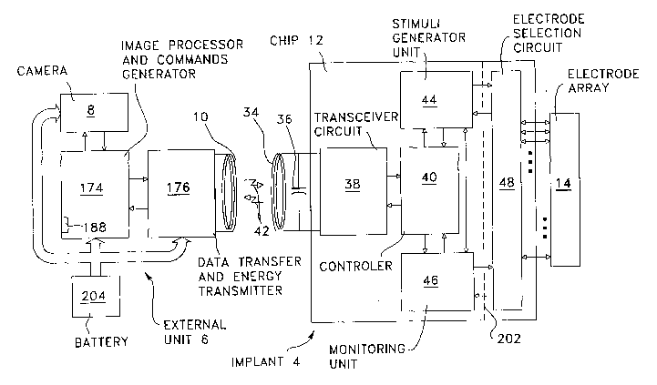
Referring to Figure 21, there is shown a body implant
system worn by a user 2 according to the present invention,
in the context where the user 2 is a blind person and the
system is used to provide artificial vision to the user 2. Tt
should be understood that this context exemplifies a typical
use of the implant system according to the present invention,
and should not be taken in a limitative or restrictive sense,
as the implant system may be used in many other contexts, for
example for monitoring purposes, and especially for measuring
parameters around an electrode-neuronal tissues interface.
13
CA 02427867 2003-05-05
WO 02/40095 PCT/CA00/01374
The body implant system includes two main parts: an
implant 4 positioned on the visual cortex of the user 2, and
an external unit 6 that can be inserted in a pocket and which
acquires real life scenes, processes the image information
and communicates with the implant 4 to provide energy for
powering the implant 4 and to control it in order to
stimulate the visual cortex of the user 2 through an
electrode array used to generate phosphenes in the visual
field corresponding to a transposition of the real life
scenes. The real life scenes can be acquired through a camera
8 (e.g. a CMOS image sensor) mounted on an earpiece of an
eyeglass, while the implant energy and control signals can be
transmitted through an inductive link using an antenna 10
positioned behind the head of the user 2.
Referring to Figures 1-6, there are shown two
embodiments of the body implant assembly according to the
present invention. These embodiments feature integration of
most of the electronic components of the implant in a,,single
full custom mixed-signal chip 12, thereby reducing power
consumption and size of the circuit. Furthermore, a special
interconnection circuit is provided for interconnection of
the chip 12 with a high resolution electrode array 14 having
multiple adjacent electrodes 16, e.g. a 25 x 26 array - 650
electrodes made of biocompatible materials, having an average
height of approx. 1, 5 mm, spaced by' approx. 400 pm from one
another and extending over a very small area, e.g. 1 cm~. The
resulting implant assembly is thus highly miniaturized
compared to prior art implants, and the interconnection
circuit provides individual connections to every electrode
16. The electrode array 14 can be made of several smaller
electrode arrays assembled together (not shown), instead of a
larger single array if desired.
Referring to Figures ~1-3, the chip 12 is embedded on a
side of a very thin substrate support 14 having contacts 17
14
CA 02427867 2003-05-05
WO 02/40095 PCT/CA00/01374
lying around the chip 12, at a given distance therefrom.
These contacts 17 are respectively connected to the pads 18
of the chip 12 for example by a wire bond 24. The other side
of the substrate support 14 is provided with an array of
adjacent contacts 20 aligned with and connected to the
electrodes 16 respectively. The connection of the contacts 20
with the electrodes l6.can be achieved by cold welding or any
other suitable technique. The contacts 17 and 20 on both
sides of the substrate support 14 are interconnected
respectively together by an interconnection circuit 22 across
the substrate support. Depending on the number of links to
achieve, the interconnection circuit 22 may be formed of
layers made in the substrate support 14 and stacked between
the sides thereof. To reduce the space taken by the contacts
17, they may be distributed in an alternate shifted pattern
over two or more adjacent sets of rows surrounding the chip
12. The body implant assembly resulting from this embodiment
is thus very thin for a reasonable cross section. An antenna
34 extends on the substrate support 14 around the chip 12 for
communication with the external unit 6. The antenna 34 is
connected to pads 18 of the chip 12 assigned for this
purpose. A capacitor 36 is coupled to the antenna 34 for
proper operation. Other suitable antenna configurations may
be used.
Referring to figures 4-6, the substrate support 14 may
be formed of a front relatively flat portion 26 having
however a smaller cross section than the substrate support 14
in the former embodiment, and a smaller rear portion 28
projecting behind the front portion and receiving the
electrode array 14. As in the former case, the contacts 17 on
the foremost face of the front portion 26 are connected
respectively to the pads 18 of the chip 12. The contacts 17
however also project through and appear behind the front
portion 26. The interconnection circuit in this case has a
CA 02427867 2003-05-05
WO 02/40095 PCT/CA00/01374
series of peripheral contacts 30 surrounding the array of
adjacent contacts 20 on the rearmost face of the rear portion
28, The peripheral contacts 30 and the contacts 17 appearing
behind the front portion 26 are respectively connected
together by a wire bond 32. Circuit layers of suitable
designs made in the rear portion 28 and stacked between the
rearmost and foremost face thereof interconnect the
peripheral contacts 30 with the array of adjacent contacts 20
respectively. The body implant assembly resulting from this
embodiment is thus thicker than in the former embodiment, but
as a smaller cross-section.
In both of the above embodiments, the body implant
assembly can be made from a silicon die containing all the
electronic circuitry necessary to receive command words,
detect and correct transmission errors, decode the command
words and control the stimulation process accordingly.
Referring to Figure 7, the full custom mixed-signal chip
12 preferably integrates a FM bi-directional data transfer &
energy receiver 38, a controller 40, a stimuli generator unit
44, an optional but generally desirable monitoring unit 46,
and depending on the chosen design, an electrode selection
circuit 48 or not as it can also be provided as a separate
circuit from the chip 12 as depicted by the dotted lines 202,
then forming another full custom chip.
The receiver 38 recovers high frequency AC signal from
the implant control signal emitted by the external unit 6,
and transforms it to a DC voltage. This.DC voltage is used to
power up the whole implant. The receiver 38 recovers also
clock and data from the same implant control signal emitted
by the external unit 6, and transmits it to the internal
controller 40. The receiver 38 gets feedback data from the
internal controller 40 and transmits it to the user through
the inductive link depicted by arrows 42. The receiver 38
thus acts as a transceiver. Although the feedback function is
16
CA 02427867 2003-05-05
WO 02/40095 PCT/CA00/01374
likely to be indispensable in most applications, it can
nevertheless be omitted if it is really useless for a
specific application.
The controller 40 decodes the commands generated by the
external unit 6 in order to produce all control signals to
the stimuli generator unit 44 and the monitoring unit 46.
Referring to Figure 8, the controller 40 may be embodied
by a circuitry mainly containing 12 units, which are grouped
into 3 main sections: a main controller module 50, a
stimulation controller module 52, and a diagnosis controller
module 54. The main controller module 50 detects data frames
and corrects communication errors, if present, in order to
build the command words used by the other modules in the
controller 40. This can be achieved through a serial/parallel
converter & frame detector 56 and an error correction &
command word decoder 58.
A power management module 60 (PMMj can be provided to
turn other modules, units, or stimulation channels on or off
individually to keep power consumption to a minimum at any
given time. Only the PMM 60 itself and the two previous
modules 56, 58, necessary for command reception, are not
susceptible to being turned off. Turning a module off means
lowering its power consumption down to zero, but does not
imply a real shut down of the unit, keeping programmed
parameters valid where volatile memory is used. For sake of
clarity, only few of the many control lines to the
controller's internal modules are presented in Figure 8.
A configuration controller 62 preferably keeps every
communication, stimulation, and diagnosis parameter
programmed by the user by means of registers CRO-CR8, and
makes them available for other modules or units. A Power-On-
Reset function controlled by the main controller 50 can be
implemented..
17
CA 02427867 2003-05-05
WO 02/40095 PCT/CA00/01374
A proper knowledge of the communication protocol for the
implant as set forth hereinafter might be important for
understanding the following part.
The stimulation controller module 52 has a Random Access
Memory 64 (RAM) intended to keep a stimulation channel/site
address sequence programmed by the external unit 6 during the
configuration process.
A stimulation commands generator 66 (SCG) decodes the
stimulation instructions and sends the required control
signals to the stimuli generator unit 44 (as shown in Figure
7), according to programmed shared stimulation parameters, if
applicable.
A clock signal 68 whose frequency depends on a specific
programmed parameter SCTB stored in the register CR3 is used
for stimulation by the stimuli generator unit 44 and is
generated by a stimulation clock module 70.
The diagnosis controller module 54 has a monitoring
commands generator 72 (MCG) which decodes the diagnosis
instructions related to the analog monitoring of the
stimulation system and electrode/tissue condition, and sends
the required control signals to the monitoring unit 46 (as
shown in Figure 7), according to the programmed
options/parameters.
A clock signal 74 whose frequency depends on a specific
programmed parameter MCTB stored in the register CR5 is used
for monitoring purposes by~the monitoring unit 46 and is
generated by a monitoring clock module 76.
A diagnosis controller 78 (DC) transmits test vectors
sent by the external unit 6 upon request to any module and
units, and receives test results thereof, both from digital
tests and from analog monitoring performed by the monitoring
commands generator 72. The DC 78 also sends the results back
to the external unit 6, via parity insertion & return word
encoder and para11e1/serial converter modules 80, 82. For
18
CA 02427867 2003-05-05
WO 02/40095 PCT/CA00/01374
sake of clarity, only a few of the many control lines to the
controller's internal modules are presented in this Figure 8.
Referring to Figure 9, the stimuli. generator unit 44 may
be embodied by a circuitry composed of 25 individual and
independent channel stimuli generators 84 (CSG). Each of the
CSG 84 has a channel controller 86 (CC), a timer module 88
and a current digital to analog converter 90 (DAC).
Two sets of registers 92, 94 allow to load the next
stimulation parameters while the current ones are used,
thereby eliminating delays between two successive
stimulations. Not shown are the diagnosis signals to/from the
controller's diagnosis controller module 78 (see Figure 8)
for testability and the power management control signals from
the power management module 60.
Referring to Figure 10, the monitoring unit 46 may be
embodied by a circuitry having the necessary sources and
measurement modules to perform real/time continuous
stimulation supervision and detailed voltage/current/complex
impedance measurement for detailed diagnosis.
During normal stimulation, conti~iuous monitoring can be
performed by constantly comparing the peak voltage Vpk across
any monitored stimulation site PrbO, Prb1 to a maximum
reference voltage VRef, through comparator 96. If the
monitored voltage exceeds the reference, the channel over-
flow signal ChanOF is activated and the channel on which the
problem arose is stored in a register 98 DefChan. The
reference signal VRef is set by the maximum allowed current
and impedance between any stimulation site monitored by the
DAC 100 and in accordance with the parameter CalRes stored in
the register CR6 of the configuration controller 62 shown in
Figure 8 and sent to the calibration channel decoder 102
shown in Figure 11.
Many options are available for detailed diagnosis. The
source may be either internal, then using the DAC 100 for
19
CA 02427867 2003-05-05
WO 02/40095 PCT/CA00/01374
this purpose, or external and then using any of the channel's
DAC 90 shown in Figure 9, as selected by the MonSrc signal
produced by the demultiplexer 104 and operating the
transistor arrangements 106 shown in Figure 11. A waveform
shaper 108 may be used to provide an unaltered square wave or
a sine shaped wave for testing purposes. An output stage 110
provides the electrode array 14 with a stimulation current
MonStim transmitted to the transistor arrangements 106 and
provides the monitoring circuit 46 with an accurate voltage
dependent copy of the stimulation current, which may be
measured via a current controlled oscillator 112, whose range
can be modified according to the input signal level OscRng
derived from the parameter OCR stored in the register CR7 of
the configuration controller 62 shown in Figure 8. Any
sampled voltage across the monitored site can be measured
with the same oscillator 112 through a transconductance
amplifier 114 with variable gain for various input voltage
ranges as set by the signal GmRng. The peak magnitude of the
voltage across the monitored site can be measured by means of
a peak detector 116. The phase between the stimulation
current and the monitored voltage can be measured through a
phase detector 118 and a frequency and phase estimator 120
for complex impedance measurements. A monitoring unit
controller 166 controls most of the components of the
monitoring unit 46 in accordance with the various control
signals produced by the monitoring commands generator 72 (see
Figure 8). A sample and hold circuit 168 is provided for the
transconductance measurement.
Not shown are the diagnosis signals to/from the
controller's diagnosis controller 78 (see Figure 8) for
testability and the power management control signals from the
power management module 60.
It should be noted that in the case where the implant 4
is intended to be used solely for monitoring purposes, then
CA 02427867 2003-05-05
WO 02/40095 PCT/CA00/01374
all the circuits of the implant 4 with functions only related
to the generation of stimulation signals can be removed from
the implant 4 inasmuch as no stimulation signals are
required. Such is the case when the implant 4 is used for
example to monitor certain body organs producing measurable
electric signals to be monitored. For example, the DACs 90
and 100 (see Figure 10), and the stimulation commands
generator 66 (see Figure 8) can be omitted in such a case.
Referring to Figure 11, the electrode selection circuit
48 can be embodied by a multiplexor/demultiplexor circuitry
comprising 25 selection channels 122 provided with channel
decoders 126 for activating up to 25 sites simultaneously.
Each site can be activated in both directions by means of
switch arrangements 124, depending on the sign bit (signal
Sign #x) for every channel.
A test channel decoder 128 selects which channel has to
be monitored. When a specific channel is monitored, the
current from the corresponding channel stimuli generator 84
in the stimuli generator unit 44 is deviated to the
monitoring unit 46 through the MonSrc line 130 and the
stimulation current comes from that latter unit through the
MonStim line 132. The channel stimuli generator 84 is
notified that its channel is being monitored with the
MonChan#x signal transmitted to corresponding the channel
controller 86.
The electrode selection circuit 48 may be provided with
a calibration channel circuit formed of the channel decoder
102 and a calibration network 134 and used by the analog
monitoring unit 46. The calibration channel decoder 102
selects an appropriate known resistive element value. This is
also used in the continuous monitoring process, generating
the appropriate reference limit voltage VRef.
21
CA 02427867 2003-05-05
WO 02/40095 PCT/CA00/01374
Sets of analog multiplexers 136 provide the monitoring
unit 46 with the voltage across any pair of electrodes
through the PrbO and Prb1 lines 138, 140.
Referring to Figure 12, there is shown a possible format
of a communication protocol for the body implant according to
the present invention. In the illustrated case, the command
words 142 are 26 bits long or less and are composed of three
parts, the mode identification bits 144,the instruction 146
and the data 148. Note that each instruction 146 can contain
one or several parts, depending on the selected mode.
A session usually starts with a configuration process.
Then the stimulation period can start, according to the
programmed configuration parameters 148 transmitted by the
external unit 6. If a problem arises, the diagnosis mode
allows a monitoring of both analog and digital components of
the system. Finally, at any time, the power management'mode
enables the external unit 6 to turn on or off any component
for reduced power consumption.
The configuration mode set by the command word <1,0> _
00 allows to define several variable parameters related to
stimulation or monitoring.
The first five configuration registers CRO to CR4 of the
configuration controller 62 (see Figure 8) define the
communication protocol during stimulation. The next four
registers CR5 to CR8 define many diagnosis parameters, the
first three being dedicated to the analog monitoring and the
last one relating to digital diagnosis of the system.
Referring to Figure 13, the definition of the parameters
in the registers CRO-CR8 is as follows. The Partial
Stimulation Word Chain Length (PSWCL) parameter defines the
number of sequential stimulation words that are sent without
interruption. The Amplitude Flag (AF) parameter defines
whether the stimulation current amplitude is specific or
common for every site. The Amplitude Word Length (AWL)
22
CA 02427867 2003-05-05
WO 02/40095 PCT/CA00/01374
parameter defines the number of bits specifying the amplitude
of the stimulation current. The Pulse Duration Flag (PDF)
parameter defines if the stimulation current pulse duration
is specific or common for every site. The Pulse Duration Word
Length (PDWL) parameter defines the number of bits specifying
the pulse duration of the stimulation current. The Interphase
Duration Flag (IDF) parameter defines if the delay between
the two phases of the stimulation current is specific or
common for every site. The Interphase Duration Word Length
(IDWL) parameter defines the number of bits specifying the
delay between the two phases of the stimulation current. The
Common Amplitude (CAMP) parameter defines the amplitude, of
the stimulation current if this parameter is common for every
site. The Common Pulse Duration (CPD) parameter defines the
pulse duration of the stimulation current if this parameter
is common for every site. The Common Interphase Duration
(CID) parameter defines the delay between the two phases of
the stimulation current if this parameter is common for every
site. The Stimulation Clock Time Base (SCTB) parameter
defines the frequency of the stimulation clock 70 shown in
Figure 8. The Stimulation Sequence Channel (SSC) and the
Stimulation Sequence Site (SSS) parameters are used to fill
the Stimulation Sequence RAM 64 shown in Figure 8. The Low
Pass Filter Cut-off Frequency (LPFCF) parameter defines the
cut-off frequency of the Gm-C low-pass filter 150 shown in
Figure 10 in the monitoring unit 46. The Monitoring Clock
Time Base (MCTB) parameter defines the frequency of the
monitoring clock 76 in the controller 40 (see Figure 8). The
Monitoring DAC Amplitude (MDACA) parameter defines the
amplitude of the output current of the DAC 90 (Figure 9) for
continuous monitoring. The Calibration Resistor (CALRES~)
parameter defines the reference equivalent resistor in the
calibration network 134 for continuous monitoring (see
Figure 11). The Transconductance Range (GMR) parameter
23
CA 02427867 2003-05-05
WO 02/40095 PCT/CA00/01374
defines the gain of the transconductance amplifier 114 (see
Figure 10). The Oscillator Current Range (OCR) parameter
defines the input current range of the current controlled
oscillator 112 (see Figure 10). The Unit/Module Under Test
(UMUT) parameter defines the unit or module under test for
digital diagnosis. The Scan Chain Length (SCL) parameter
defines the number of bits of the scan chain in the unit or
module under test. The Stimulation clock Sync (SS) parameter
synchronizes the stimulation clock 70 (Figure 8). The
Monitoring clock Sync (MS) parameter synchronizes the
monitoring clock 76 (Figure 8). The RAM Reset (RR) parameter
resets the address pointer of the Stimulation Sequence RAM
64 (Figure 8) to zero. The Continuous Monitoring (CM)
parameter turns the continuous monitoring feature of the
controller 40 (Figure 7) on/off.
Referring to Figure 14, in the stimulation mode set by
the command word <1,0> -- Ol, the instruction 152 depends
directly on the stimulation communication protocol defined in
the configuration. The instruction 152 is sent as a chain of
a certain number (PSWCL) of stimulation words, each
containing 1 to 34 bits, depending on the common parameters.
If the chain is longer than 24 bits, it is divided into
sequential stimulation instruction words of 24 bits or less
for the last word.
Referring to Figure 15, the diagnosis mode set by the
command word <1,0> _- 10 allows detailed and various analyses
of the condition of the system, on both the digital and
analog sides. When the first bit of the diagnosis instruction
word 154 is set in a low state 156, the following data is
used to determine the information required for analog
monitoring. The instruction is then composed of: a Monitored
Site (MS) parameter, a Monitored Channel (MC) parameter, a
Monitoring current Amplitude (MAMP) parameter, and a
Monitoring Options (MOPT) parameter. The MOPT parameter
24
CA 02427867 2003-05-05
WO 02/40095 PCT/CA00/01374
specifies what the stimulation source is, what the
stimulation waveform is, if the measured value is a current,
if the measured value is a voltage, and if the measured value
is the phase between current and voltage.
When the first bit of the diagnosis instruction word 154
is set in a high state 158, the diagnosis concerns the
digital system. To input a test vector, the next bit is set
to a low state and the vector 160 itself follows. If the
length of the test vector is longer than 22 bits as defined
by the SCL parameter in the configuration mode, the 23rd and
next bits are sent in a subsequent similar diagnosis
instruction word.
To read the data in a particular module of the system,
both the first and second bit of the diagnosis instruction
word are set in a high state 162. The controller will then
send the test result back to the external unit 6.
Referring to Figure 1.6, the power management mode set by
the command word <1,0> _- 11 allows to turn any component of
the system on and off. The two parameters supplied in this
mode are the power management action (PA), which defines if
the unit/module has to be turned on/off, and the unit/module
identification (MID) that defines which unit/module the power
management action has to be applied to.
.As mentioned hereinabove, the stimulation biphasic
current pulses used to generate a phosphene can be described
by three parameters, which are the amplitude, the phase
duration and the inter-phase duration of the pulses. Each one
of theses parameters, as well as the pulse frequency,
influences the phosphenes visual appearance. It would require
a high data transmission rate to send in real time all the
stimulation parameters as well as the addresses of the
corresponding stimulation sites from the external unit 6 to
the implant 4. In order to reduce this rate, the needed
stimulation data can be transferred as follows. First, each
CA 02427867 2003-05-05
WO 02/40095 PCT/CA00/01374
of the parameters is, beforehand, defined to be common or
specific. A common parameter is shared by all the stimulation
sites and has to be loaded only once at the beginning.
However, the specific parameters have to be updated at each
activation site. As an example, the phase and inter-phase
durations can be common, and the amplitude can be specific.
Using one or two common parameters allows a significant
reduction in the transmission rate between the external unit
6 and the implant 4. The choice of which parameters are
common or specific, as well as the number of bits necessary
to specify each one of them can be set at any time in the
configuration mode.
Secondly, instead of sending the stimulation site
address with each parameter, the RAM 64 (figure 8) is used.
During the configuration phase of the implant 4, the external
unit 6 fills the memory 64 with the scan sequence of each
frame in an image that will be used by both devices (the
implant 4 and the external unit 6). The stimulation
parameters are then sent in the order specified in the memory
64.
This kind of transfer of the needed data makes the
implant 4 highly configurable, allowing the external unit 6
to fully control the stimulation operations and allowing a
higher frame (image) transmission rate, if needed.
Referring to Figure 8, in operation, the stimulation
commands generator 66 combines the common parameter data with
each specific stimulation word to generate the proper
stimulation control signals for the stimuli generator unit
44, indicating in particular the amplitude of the biphasic
pulse (StimAmp), the phase duration of the pulse (PhaseDur),
the interphase duration of the pulse (InterDur), the
stimulation site address (StimSite), the stimulation channel
number (StimChan).
26
CA 02427867 2003-05-05
WO 02/40095 PCT/CA00/01374
Referring to Figure 9, when a particular channel
controller 86 receives the stimulation control signals, it
loads the data into the set of temporary registers 92. Once
the previous stimulation is completed, the data are
transferred into the main registers 94 as a result of a
control performed by the channel controller (Idnp and Idcp
signals). The DAC 90 is responsive to the channel controller
86 (Stim signal) and generates a stimulation current having
an amplitude depending on the StimAmp value. The stimulation
operation begins using the site address bus 164 to select the
proper site in the channel and the Stim signal to start and
stop stimulation. The channel controller 86 uses the timer 88
based on the stimulation clock 70 (Figure 8) to set the phase
and interphase durations of the pulses.
Referring to Figure 7, the external unit 6 has an image
processor and command generator module 174 connected to the
camera 8 for processing image data signals corresponding to a
real life scene captured by the camera 8, in accordance with
predetermined processing operations, and for generating
implant compatible stimulation commands causing the implant 4
to produce the artificial image on the visual cortex
corresponding to the real scene image. A transceiver module
176 preferably in the form of a FM bi-directional data
transfer and energy transmitter is connected to the image
processor and command generator module, for producing
airwave-transmitted implant control signals carrying the
stimulation commands, as depicted by the arrows 42. The
external unit 6 is preferably powered by a battery 204.
Referring to Figures 7 and 17, the processing operations
performed by the image processor and commands generator 174
on the real life scene 170 subjected to acquisition 178 by
the camera 8 can be a digitalization of the image data
signals to form a digital image 180, an image reduction of
the digital image 180 into a scaled down image 182 having a
27
CA 02427867 2003-05-05
WO 02/40095 PCT/CA00/01374
same resolution as the electrode array 14, and an image
enhancement of the scaled down image 14 to form an enhanced
image 184 corresponding to the artificial image produced by
the implant unit 4 and from which the stimulation commands
186 are generated.
The external unit 6 may be provided with a pattern
generation interface (not shown) where the command words are .
formed from internal patterns instead of the image sensor 8.
Such a feature would allow to quickly test recognizable
patterns like a square, a circle or a cross for adjustment of
the implant 4 to the user 2.
Once the image 182 has the proper resolution, basic
image enhancement techniques are preferably applied. The
purpose of the enhancement is to give to the image more
balanced contrasts and luminosity. The applied technique can
be a linear histogram equalization consisting of stretching
the image histogram to cover the totality of the available
pixel intensity spectrum. It is not necessary to calculate
the whole histogram since only the minimum and maximum pixel
intensities are useful. With those values, a look-up table
can be built to transform, one by one, each pixel of the
initial image.
Figures 18A-B and 19A-B illustrate scaled-down and
enhanced images generated by the image processor 174
(Figure 7), and the corresponding histograms respectively. As
it can be seen, the histogram shown in Fig. 19B,
corresponding to the enhance image shown in Figure 19A,
covers a wider spectrum than the histogram shown in Figure
18B for the image prior to enhancement as shown in Figure
18A.
After the image enhancement, each pixel of the resulting
image will represent a phosphene that should be created
during the cortex stimulation. To create this phosphene, a
command word must be created to specify every stimulation
28
CA 02427867 2003-05-05
WO 02/40095 PCT/CA00/01374
parameter, from waveform shape to phase delay. Since many of
the parameters affect only the qualitative, part of phosphene
appearance and the effects of their modification is not
currently thoroughly known, those parameters must be easily
and quickly alterable. In addition, when stimulating
biological cells with an electrical current, the stimulation
of the same cells, or cells in the surrounding, cannot be
repeated before a delay of few ms. This delay is called
repolarization time. For this reason, serial scanning cannot
be used for the stimulation of the cortex in order to create
an image. Instead, a scan sequence must be selected in such a
way that each sequential stimulation is not executed in an
area where a stimulation occurred before the repolarization
time is elapsed. The flexibility of the implant system
according to the invention allows the use of any desired
scanning sequence and the configuration of the implant 4 with
the same sequence.
Referring to Figure s 7 and 20, the external unit 6 may
be provided with a communication-port 188 for communication
with a computer (not shown) for configuration and test
purposes. For example, to test the system, easily
recognizable shapes may be used to test the phosphene
apparition parameters, as mentioned hereinabove. Those shapes
can be generated by the external unit 6 in response to a test
request issued by the computer, as inputted through a user
interface 190. The user can select different patterns 192 and
adjust the parameters 194 on the fly. For example, a square,
a cross or a circle may be selected, each of which can be in
a solid or outline form. Character generation can also be
implemented to enable more complex shapes. For greater user
control, those patterns may bypass the usual data pathway and
directly generate the command words in the external unit 6.
The user interface 190 may display a source image 196 as
captured by the camera 8 or from another source, and the
29
CA 02427867 2003-05-05
WO 02/40095 PCT/CA00/01374
corresponding image 198 reduced to the resolution of the
electrode array 14, in its enhanced form. The reduced image
resolution can be changed instantly within the drop down menu
list 200.
Referring to Figure 7, the camera 8 has preferably a
variable resolution providing an electronic zoom function.
Such a feature can be used to adapt the low resolution of the
image transmitted to the implant 4 (e.g. 25 x 25) to the
situation in which the user is. For example, the user may
choose between a coarse view over a large field of vision or,
conversely, a detailed view over a limited zone in order to
discern the details of a point of. interest or for reading
purposes.
Instead of using a predetermined addressing process
using the RAM 64 (see Figure 8) as hereinabove described,
which allows to reduce the pass-band of the transmitted data
when the stimulation sequence and the pixel numbers are
constant for each image, a specific addressing process can
also be implemented to allow the stimulation sites to be
chosen according to each image to be transmitted. Then, by
setting a light intensity threshold under which the
stimulation effect is considered to be negligible, certain
pixels of the image will be simply disregarded by the
external unit 6. As a result, power consumption can be
thereby reduced while the image refresh rate is improved.
Preferably, the threshold is adjustable in order to
discriminate the pixels to be transmitted from those to be
discarded. Other suitable addressing methods can also be
implemented.
The implant system according to the invention can be
equipped for example with an ultrasound sensor (not shown)
having a large field of detection, preferably set as a
function of the minimum zoom of the camera 8 or larger,
providing information on the proximity of detected objects,
v
CA 02427867 2003-05-05
WO 02/40095 PCT/CA00/01374
which information affects the light intensity transmitted to
the brain. Such a system would allow the user to move
smoothly by following the dark or clear zones that he or she
sees, without requiring Visual recognition of the surrounding
objects, which may be difficult to achieve at a low
resolution (e. g. 25 x 25).
While embodiments of this invention have been
illustrated in the accompanying drawings and described above,
it will be evident to those skilled in the art that changes
and modifications may be made therein without departing from
the essence of this invention. All such modifications or
variations are believed to be within the scope of the
invention as defined by the claims appended hereto.
31