Note : Les descriptions sont présentées dans la langue officielle dans laquelle elles ont été soumises.
CA 02429430 2003-05-23
BALLAST WITH LAMP-TO-EARTH-GROUND FAULT
PROTECTION CIRCUIT
Field of the Invention
The present invention relates to the general subject of circuits for
powering discharge lamps. More particularly, the present invention relates to
a
ballast with circuitry for protecting against a lamp-to-earth-ground fault
condition.
Background of the Invention
Fluorescent lamps used with electronic ballasts periodically fail and
require replacement. In most cases, replacement of a failed lamp is performed
while AC power is still applied to the ballast; this practice is sometimes
referred
to as "live relamping." Since many newer ballast designs have non-isolated
outputs, the possibility exists for high frequency output current to travel
from
the ballast output, through the lamp, through the person replacing the lamp,
to
fixture ground. Because an electrical shock may be suffered under such
circumstances, safety agencies such as Underwriters Laboratories now require
that ballasts be tested for this condition. Thus, standards have been
established
for the maximum current that is allowed to flow from the ballast output
through
the lamp to fixture ground. For many ballasts, these standards are readily
met.
However, for some ballasts, such as those models which are designed to operate
with higher line voltages (e.g., 277 volts) or shorter lamp lengths (e.g., 2
foot
lamps), these standards can be met only by incorporating special protective
circuitry in the ballast.
Some ballast manufacturers have attempted to address the problem of
excessive lamp-to-earth-ground current by trying to sense the high frequency
leakage current that, in the event of a fault condition, flows out of the
ballast
output, into the grounded fixture, and back into the ballast via the ballast
ground
wire that is electrically connected to the fixture during ballast
installation. An
example of such an approach is described in U.S. Patent 5,363,018. The main
problem with this type of detection circuit is that this same type of leakage
CA 02429430 2010-11-29
2
current normally flows even in the absence of a fault condition, and is
actually quite
desirable because it aids lamp ignition. Moreover, because the voltage applied
to the lamps
prior to ignition is much higher than voltage applied after ignition, the
magnitude of this
"normal" leakage current will be many times higher during the start-up mode
than during
the steady-state operating mode. Because the magnitude of the normal leakage
current that
flows into the ballast ground during normal starting conditions can be very
close to the
magnitude of the undesirable leakage current that flows through the body of a
person who
accidentally touches the ballast output and fixture ground, the prior art
circuits cannot
accurately discriminate between "normal" leakage current and the leakage
current that
occurs due to a true fault condition.
Summary of the Invention
What is needed, therefore, is a ballast with a protection circuit that is
capable of
more reliably detecting a lamp-to-earth-ground fault condition. A ballast with
such a
protection circuit would represent a significant advance over the prior art.
In accordance with one aspect of the present invention, there is provided a
ballast for
powering at least one gas discharge lamp, comprising: an inverter for
supplying a high
frequency alternating current to the gas discharge lamp; first, second, third,
and fourth
output connections adapted for connection to the gas discharge lamp, wherein
the first and
second output connections are adapted for connection to a first filament of
the lamp, and the
third and fourth output connections are adapted for connection to a second
filament of the
lamp; and a protection circuit coupled to the inverter and the first, second,
third, and fourth
output connections, the protection circuit comprising: a transformer,
comprising: a first
primary winding coupled in series with the first output connection; a second
primary
winding coupled in series with the second output connection; a third primary
winding
coupled in series with the third output connection; a fourth primary winding
coupled in
series with the fourth output connection; and a secondary winding operably
coupled to the
inverter, the secondary winding having a voltage that is: (i) substantially
zero in the absence
of a lamp-to-earth-ground fault condition; and (ii) nonzero in the presence of
a lamp-to-
earth-ground fault condition.
In accordance with another aspect of the present invention, there is provided
a
ballast for powering at least one gas discharge lamp, comprising: an inverter
for supplying a
high frequency alternating current to the gas discharge lamp, the inverter
including an
inverter drive circuit having a voltage supply input for receiving a supply
voltage, the
CA 02429430 2010-11-29
3
inverter drive circuit being operable to: (i) provide inverter switching as
long as the supply
voltage is greater than a predetermined shutdown voltage; and (ii) cease to
provide inverter
switching when the supply voltage falls below the predetermined shutdown
voltage; first,
second, third, and fourth output connections adapted for connection to the gas
discharge
lamp, wherein the first and second output connections are adapted for
connection to a first
filament of the lamp, and the third and fourth output connections are adapted
for connection
to a second filament of the lamp; and a protection circuit coupled to the
inverter and the first,
second, third, and fourth output connections, the protection circuit
comprising: a
transformer comprising: a first primary winding coupled in series with the
first output
connection; a second primary winding coupled in series with the second output
connection;
a third primary winding coupled in series with the third output connection; a
fourth primary
winding coupled in series with the fourth output connection; and a secondary
winding
operably coupled to the inverter; an inverter disable circuit that includes
the secondary
winding of the transformer and that is coupled to the voltage supply input of
the inverter
drive circuit, the inverter disable circuit being operable, in response to a
nonzero voltage
across the secondary winding of the transformer, to terminate inverter
switching by
coupling the voltage supply input to circuit ground; and a restart timer
circuit coupled to the
inverter, the restart timer circuit being operable, following termination of
inverter switching,
to prevent the inverter from resuming inverter switching for at least a
predetermined restart
period.
In accordance with another aspect of the present invention, there is provided
a
ballast for powering at least one gas discharge lamp, comprising: first,
second, third, and
fourth output connections adapted for connection to the gas discharge lamp,
wherein the
first and second output connections are adapted for connection to a first
filament of the lamp,
and the third and fourth output connections are adapted for connection to a
second filament
of the lamp; an inverter for supplying a high frequency alternating current to
the gas
discharge lamp, the inverter comprising: an inverter drive circuit having a
voltage supply
input for receiving a supply voltage, the inverter drive circuit being
operable to: (i) provide
inverter switching as long as the supply voltage is greater than a
predetermined shutdown
voltage; and (ii) cease to provide inverter switching when the supply voltage
falls below the
predetermined shutdown voltage; and a bootstrap power source that is operable,
while
inverter switching is occurring, to provide power to the inverter drive
circuit; and a
protection circuit, comprising: a transformer, comprising: a first primary
winding coupled in
series with the first output connection; a second primary winding coupled in
series with the
CA 02429430 2010-11-29
4
second output connection; a third primary winding coupled in series with the
third output
connection; a fourth primary winding coupled in series with the fourth output
connection;
and a secondary winding; an inverter disable circuit, comprising: a disable
output coupled to
the voltage supply input of the inverter drive circuit; a transistor having a
base, a collector,
and an emitter, wherein the emitter is coupled to circuit ground; the
secondary winding of
the transformer, the secondary winding being coupled between a first node and
circuit
ground; a first resistor coupled between the first node and circuit ground; a
diode coupled
between the first node and the base of the transistor; a capacitor coupled
between the base
of the transistor and circuit ground; a second resistor coupled between the
base of the
transistor and circuit ground; and a third resistor coupled between the
disable output and the
collector of the transistor; and a restart timer circuit, comprising: a
restart input coupled to
the bootstrap power source of the inverter; a restart output coupled to the
voltage supply
input of the inverter drive circuit; a transistor having a collector, an
emitter, and a base,
wherein the emitter is coupled to circuit ground; a series combination of a
diode and a first
resistor coupled between the restart input and a second node; a capacitor
coupled between
the second node and circuit ground; a second resistor coupled between the
second node and
the base of the transistor; a third resistor coupled between the base of the
transistor and
circuit ground; and a fourth resistor coupled between the restart output and
the collector of
the transistor.
Brief Description of the Drawings
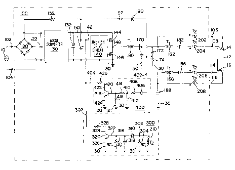
FIG. 1 describes a ballast with a lamp-to-earth-ground fault protection
circuit, in
accordance with a preferred embodiment of the present invention.
FIG. 2 describes a portion of a ballast adapted to power two gas discharge
lamp, in
accordance with a preferred embodiment of the present invention.
Detailed Description of the Preferred Embodiments
In a preferred embodiment of the present invention, as described in FIG. 1, a
ballast
100 for powering at least one gas discharge lamp 12 includes an inverter
140,144,146,148,
output connections 106,108,114,116, and a protection circuit
202,204,206,208,210,300,400.
Preferably, ballast 100 further includes a pair of input connections 102,104
adapted to
receive a conventional source of alternating current (e.g., 120 VAC at 60
Hertz), a full-wave
diode bridge rectifier 120, a high frequency bypass capacitor 122, a boost
converter 130,
and a bulk capacitance 132.
CA 02429430 2010-11-29
4a
The inverter is preferably implemented as a driven half-bridge
140,144,146,148. In
combination with a direct-coupled series resonant output circuit 160,170, the
inverter
supplies a high frequency (e.g., greater than 20 kilohertz) alternating
current to gas
discharge lamp 12 via first, second, third, and fourth output connections
106,108,114,116.
The inverter includes an inverter drive circuit 140 having a voltage supply
input 142 for
receiving a direct current (DC) supply voltage. Upon initial application of AC
power to
ballast 100, capacitor 150 charges up via resistor 152. Once the voltage
across capacitor 150
reaches a predetermined startup threshold (e.g., 10 volts), inverter drive
circuit 140 starts
and begins to switch inverter transistors 144,146 on and off in a
substantially
complementary manner. Inverter drive circuit 140 continues to provide inverter
switching as
long as the voltage at voltage supply input 142 remains greater than a
predetermined
shutdown threshold (e.g., 8 volts), but will cease to provide inverter
switching if the voltage
at voltage supply input 142 falls below the predetermined shutdown threshold.
During
normal operation, the voltage at voltage supply input 142 is maintained well
above the
shutdown threshold by a "bootstrapping" circuit that includes capacitor 172,
zener diode
174, diode 190, and resistor 192.
First and second output connections 106,108 are adapted for connection to a
first
filament 14 of lamp 12, while third and fourth output connections 114,116 are
adapted for
connection to a second filament 16 of lamp 12.
Protection circuit 202,204,206,208,210,300,400, which is coupled to the
inverter and
the output connections, monitors a first current and a second current. The
first current is
defined as the absolute value of the difference between the current flowing
out of first
output connection 106 and the current flowing into second output connection
108. The
second current is defined as the absolute value of the difference between the
current flowing
out of third output connection 114 and the current flowing into fourth output
connection 116.
During normal operation (i.e., when no lamp-to-earth-ground fault condition is
present), the
first and second currents will be substantially equal. During a fault
condition, the first
current will not be substantially equal to the second current. Under such a
fault condition,
the protection circuit will disable the inverter.
The protection circuit includes a transformer T2 and an inverter disable
circuit 300.
Transformer T2 comprises four primary windings 202,204,206,208 and a secondary
winding
210. First primary winding 202 is coupled in series with first output
connection 106. Second
primary winding 204 is coupled in series with second output connection 108.
Third primary
winding 206 is coupled in series with third output connection 114. Fourth
primary winding
CA 02429430 2010-11-29
4b
208 is coupled in series with the fourth output connection 116. Secondary
winding 210 is
part of inverter disable circuit 300. Preferably, first, second, third, and
fourth primary
windings have the same number of wire turns (e.g., 1 turn). Secondary winding
210 has a
number of wire turns (e.g., 30 turns) that is substantially greater than the
number of wire
turns on the primary windings. The relative orientation or polarity of the
four primary
windings is indicated by the dots depicted in FIG. 1.
During normal operation (i.e., when no fault condition is present), the first
current is
substantially equal to the second current. Correspondingly, the voltages
induced in first and
second primary windings 202,204 are cancelled out by the voltages induced in
third and
fourth primary windings 206,208. Consequently, the voltage across secondary
winding 210
will be substantially zero.
During a lamp-to-earth-ground fault condition, the first current will not be
substantially equal to the second current because a portion of the current
CA 02429430 2003-05-23
flowing out of output connections 106,108 will be diverted to earth ground
and,
thus, will not flow back into output connections 114,116. Correspondingly, the
voltages induced in first and second primary windings 202,204 will not be
cancelled out by the voltages induced in third and fourth primary windings
5 206,208. Consequently, a nonzero voltage will appear across secondary
winding 210. In this way, the voltage across secondary winding 210 indicates
the presence of a lamp-to-earth-ground fault condition.
The nonzero voltage that appears across secondary winding 210 during a
fault condition is detected by the other circuitry in inverter disable circuit
300 so
as to shut down the inverter. More particularly, in response to a nonzero
voltage
across secondary winding 210 of transformer T2, inverter disable circuit 300
terminates inverter switching by coupling the voltage supply input 142 of
inverter drive circuit 140 to circuit ground 30.
In a preferred embodiment, as described in FIG. 1, inverter disable
circuit 300 comprises the secondary winding 210 of transformer T2, a disable
output 302, a transistor 320, a first resistor 304, a diode 310, a capacitor
316, a
second resistor 318, and a third resistor 328. Secondary winding 210 and first
resistor 304 are each coupled between a first node 302 and circuit ground 30.
Disable output 302 is coupled to voltage supply input 142 of inverter drive
circuit 140. Transistor 320 has a base 322, a collector 324, and an emitter
326.
Emitter 326 is coupled to circuit ground 30. Diode 310 is coupled between
first
node 302 and the base 322 of transistor 320; more specifically, diode 310 has
an
anode coupled to first node 302 and a cathode coupled to base 322. Capacitor
316 and resistor 318 are each coupled between base 322 and circuit ground 30.
Finally, third resistor 328 is coupled between disable output 302 and emitter
324
of transistor 320.
In a prototype ballast configured substantially as shown in FIG. 1,
inverter disable circuit 300 was implemented with the following component
values:
Resistor 304: 100 kilohms
Diode 310: 1N4148
Capacitor 316: 22 micofarads
CA 02429430 2010-11-29
6
Resistor 318: 2.2 kilohms
Transistor 320: Q2N3904
Resistor 328: 10 ohms
As previously described, it is preferred that transformer T2 be implemented
with one
turn on each of the four primary windings 202,204,206,208, and with thirty
(30) turns on
secondary winding 210.
During normal operation (i.e., when no fault condition is present), the
voltage across
secondary winding 210 is approximately zero. Consequently, little or no
voltage is provided
at the base 322 of transistor 320, so transistor 320 is off. Accordingly, in
the absence of a
fault condition, inverter disable circuit 300 does not affect the normal
operation of inverter
drive circuit 140.
If a lamp-to-earth-ground fault condition occurs, a nonzero voltage will
develop
across secondary winding 210. The nonzero voltage across secondary winding 210
is peak-
detected by diode 310 and capacitor 316, which causes transistor 320 to turn
on. With
transistor 320 turned on, resistor 328 is connected between voltage supply
input 142 and
circuit ground 30. Because resistor 328 has a very low resistance (e.g., 10
ohms), it quickly
discharges capacitor 150, in spite of the fact that appreciable current
continues to be
supplied to capacitor 150 from bootstrap power source 172,174 via diode 190
and resistor
192. Consequently, the voltage at voltage supply input 142 rapidly falls below
the level
necessary to keep inverter drive circuit 140 operating, and inverter switching
ceases.
Preferably, the protection circuit further includes a restart timer circuit
400 for
keeping the inverter disabled for a predetermined restart period following
detection of lamp-
to-earth-ground fault condition. Without restart timer circuit (400), the
inverter will
automatically restart after a brief delay period (e.g., on the order of 100-
200 milliseconds)
after being disabled by inverter disable circuit 300. In order to ensure that
the average rms
fault current will be well within safety requirements, it is desirable that
the delay period be
increased considerably (e.g., to about 1.5 seconds). Restart timer circuit 300
provides such
an increased delay.
CA 02429430 2003-05-23
7
In a preferred embodiment, as described in FIG. 1, restart timer circuit
400 comprises a restart input 402, a restart output 404, a transistor 418, a
series
combination of a diode 406 and a resistor 408, a capacitor 412, a second
resistor
414, a third resistor 416, and a fourth resistor 426. Restart input 402 is
coupled
to the bootstrap power source 172,174 of the inverter. Restart output 404 is
coupled to voltage supply input 142 of inverter drive circuit 140. Transistor
418
has a collector 422, an emitter 424, and a base 420. Emitter 424 is coupled to
circuit ground 30. The series combination of diode 406 and resistor 408 is
coupled between restart input 402 and a second node 410; more specifically,
diode 406 has an anode coupled to restart input 402 and a cathode coupled to
resistor 408, wherein resistor 408 is coupled to second node 410. Capacitor
412
is coupled between second node 410 and circuit ground 30. Second resistor 414
is coupled between second node 410 and base 420 of transistor 418. Third
resistor 416 is coupled between base 420 and circuit ground 30. Finally,
fourth
resistor 426 is coupled between restart output 404 and collector 422 of
transistor
418.
In a prototype ballast configured substantially as shown in FIG. 1, restart
timer circuit 400 was implemented with the following component values:
Diode 406: I N4148
Resistor 408: 4.7 kilohms
Capacitor 412: 10 micofarads
Resistor 414: 100 kilohms
Resistor 416: 22 kilohms
Transistor 418: Q2N3904
Resistor 426: 3.3 kilohms
The detailed operation of restart timer circuit 400 is now described with
reference to FIG. 1 as follows.
During normal operation (i.e., when no fault condition is present),
capacitor 412 remains charged, via bootstrap power source 172,174 and the
series combination of diode 406 and resistor 408, at a voltage of
approximately
15 volts. A portion of the voltage across capacitor 412 is applied (via
resistors
414,416) to transistor 418, which turns on and connects restart output 404
(and
CA 02429430 2003-05-23
8
thus voltage supply input 142 of inverter drive circuit 140) to circuit ground
30
via resistor 426. When the inverter is operating normally, the loading
introduced by having voltage supply input 142 connected to circuit ground 30
via resistor 426 has no effect because resistor 426 is selected to be suitably
large
(e.g., 3.3 kilohms) and bootstrap power source 172,174 (which supplies
operating current to inverter drive circuit 140 via diode 190 and resistor
192) is
a low impedance current source that is more than capable of supplying the
additional current required by the introduction of resistor 426 while the
inverter
is operating. Thus, during normal conditions, restart timer circuit 400 does
not
affect the operation of the inverter.
When inverter drive circuit 140 is shut down by inverter disable circuit
300 in response to fault condition, the connection of resistor 426 between
voltage supply input 142 and circuit ground 30 will prevent drive circuit 300
from restarting for as long as the voltage across capacitor 412 is sufficient
to
keep transistor 418 turned on. More specifically, with resistor 426 present,
capacitor 150 will be prevented from charging up (via resistor 152) to a level
sufficient (e.g., 10 volts, which is the typical turn-on threshold of inverter
drive
circuit 140) to restart inverter drive circuit 140. With inverter drive
circuit 140
disabled, bootstrap power source 172,174 no longer supplies current to
capacitor
412, so the voltage across capacitor 412 will begin to decrease at a rate
determined by the capacitance of capacitor 412 and the resistances of
resistors
414,416. Once the voltage across capacitor 412 falls below a certain level
(e.g.,
a few volts), transistor 418 will turn off and allow capacitor 150 to charge
up
(via startup resistor 152) to a level sufficient (e.g., 10 volts) to restart
inverter
drive circuit 140. If a lamp-to-earth-ground fault condition is still present,
inverter disable circuit 300 will promptly shut down the inverter once again,
and
the aforementioned cycle will repeat itself for as long as a fault condition
is
present.
It is preferred that capacitor 412 and resistors 414,416 be sized such that
transistor 418 will remain on for about 1.5 seconds after inverter drive
circuit
300 is disabled in response to a fault condition; in a prototype ballast
configured
substantially as shown in FIG. 1, the preferred restart delay of about 1.5
seconds
CA 02429430 2011-04-01
9
was achieved with capacitor 412 set at 10 microfarads, resistor 414 set at 100
kilohms, and
resistors 416 set at 22 kilohms. Although the inverter will be allowed to
restart every 1.5
seconds even if an uncorrected fault condition remains present, the duty cycle
(and, thus, the
resulting rms value of the ground fault current) will be quite low because the
inverter will be
promptly shut down by inverter disable circuit 300.
Although the ballast 100 described in FIG. 1 has been shown as operating a
single
lamp 12, it should be appreciated that the principles of the present invention
are readily
extended to a ballast that operates multiple lamps connected in series. For
example, as
described in FIG. 2, the circuitry detailed in FIG. 1 may be adapted to a
ballast for powering
two lamps 12,22 simply by adding an additional filament winding 164 (on
transformer Ti), an
additional current-limiting capacitor 184, and additional output connections
110,112. As
illustrated in FIG. 2, output connections 110,112 are coupled to both the
second filament of
lamp 12 and a first filament of lamp 22. Output connections 114,116 are
coupled to a second
filament of lamp 22. Along similar lines, ballast 100 may be further adapted
to power three of
four series-connected lamps. For each additional lamp, an additional filament
winding,
current-limiting capacitor, and pair of output connections is required.
Although the present invention has been described with reference to certain
preferred
embodiments, numerous modifications and variations can be made by those
skilled in the art
without departing from the scope of this invention.