Note : Les descriptions sont présentées dans la langue officielle dans laquelle elles ont été soumises.
CA 02431297 2003-06-05
DESCRIPTION
SWITCHING AMPLIFIER
Technical Field
The present invention relates to a switching amplifier, which amplifies analog
signals or mufti bit digital signals, and relates to a new switching amplifier
in which power
supply switching noise is reduced to improve the quality.
Background Art
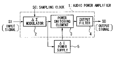
A switching amplifier comprising a conventional power amplifier is shown in
FIG.
7. This conventional example relates to a switching amplifier for audio. This
switching
amplifier is provided with an audio power amplifier l and a power supply 6,
the audio
power amplifier 1 being provided with a ~E modulator 2 for ~E modulating an
audio
signal. The construction is such that an output pulse signal from this ~E
modulator 2 is
supplied to a power switching element 3 in the amplifier, and then output via
an output
filter 4 in the amplifier. The power supply 6 is connected to this power
switching element
3 in the amplifier, the construction being such that the power supply 6
receives a clock
signal, performs pulse width modulation in synchronization with this clock
signal,
supplies this pulse width modulated signal to a power switching element in the
power
supply, and supplies required power to the power switching element 3 in the
amplifier via
an output filter in the power supply.
'This conventional example of a switching amplifier operates as follows.
Firstly, a
signal such as an audio signal or the like is input to the DE modulator 2, and
a sampling
clock is input to this ~E modulator 2 at the same time. The input signal is ~E
modulated
CA 02431297 2003-06-05
2
by the ~E modulator 2, and the output pulse signal thereof is input to the
power switching
element 3 in the amplifier. In addition, a different clock signal from the
sampling clock
signal is input to the power supply 6, pulse width modulation is performed in
synchronization with this clock signal, and the pulse width modulated output
pulse signal
is input to the power switching element in the power supply. The output of the
power
switching element in the power supply is output through an output filter 7 in
the power
supply, and supplies power to the power switching element 3 in the amplifier.
However, since the power supply 6 and the power amplifier 1 are independent
from each other in this method, there is a problem that switching noise from
the power
supply 6 easily affects the output of the power amplifier. In addition, a
large output filter
7 in the power supply must be installed at the output of the power supply so
that switching
noise from the power supply does not affect the power amplifier 1. However, a
conventional output filter 7 in the power supply is typically constructed such
that a
smoothing circuit and a noise filter are connected, and the installation of a
noise filter in
this case makes miniaturization difficult. Moreover, if construction of the
output filter 7
in the power supply is attempted excluding a noise filter, it is necessary to
enlarge a
capacitor and a choke coil that comprise the smoothing circuit. Whichever
construction is
used, since the output filter 7 in the power supply is comparatively large,
there is a
problem that it is difficult to miniaturize the switching amplifier.
Disclosure of Invention
The present invention takes the above problems into consideration, with an
object
of providing a new switching amplifier that reduces the switching noise of a
power supply,
in particular to achieve an improvement in quality.
CA 02431297 2003-06-05
To achieve the abovementioned object, in the present invention, the timing of
switching noise in the power amplifier and the power supply is almost the
same, and even
if noise from the power supply is mixed in, it is possible to use a common
noise filter in
the power amplifier. Furthermore, a noise filter for power supply is
unnecessary, and it is
also not necessary to have a smoothing circuit equipped with a comparatively
large-sized
capacitor and choke coil in the power supply output, so that it is possible to
simplify the
output filter of the power supply. Moreover, simplification of the power
supply output
filter enables the switching amplifier to be miniaturized and cost reduced.
That is, the present invention has the following construction in order to
solve the
above problems.
A switching amplifier according to a first aspect of the present invention
comprises: a switching power amplifier which has a modulator which modulates
an analog
signal or a mufti bit digital signal into a two-IeveI signal, and supplies an
output pulse
signal from the modulator to a power switching element; and a DE power supply
which
has a DE modulating device which DE modulates an analog signal or a mufti bit
digital
signal, and supplies a pulse signal for power supply control output from the
AE
modulating device to a power switching element in the power supply, wherein an
output
pulse signal of the modulator in the power amplifier is supplied to the ~
power supply,
and the output pulse signal is input as an operating clock to the DE power
supply, and the
output power of the ~E power supply is supplied to the power switching element
in the
power amplifier.
A switching amplifier according to a second aspect of the present invention
comprises: a power amplifier having at least a pair of power switching
elements in the
output stage thereof, which modulates an input signal comprising an analog
signal or a
mufti bit digital signal into a two-level signal, and obtains an output signal
power
CA 02431297 2003-06-05
4
amplified by controlling the conductivity of the power switching elements
complimentarily based on the two-level signal; and a switching power supply
which
generates a required power supply voltage to be supplied to the power
switching elements
by switching in synchronization with the two-level signal.
A switching amplifier according to a third aspect of the present invention is
that, in
a switching amplifier according to the second aspect of the present invention,
an operation
timing between the switching power supply and the power amplifier is set such
that noise
accompanying the switching operation of the switching power supply occurs
within a
predetermined period during which the power switching elements installed in
the output
stage are both off.
A switching amplifier according to a fourth aspect of the present invention is
that,
in a switching amplifier according to the second or the third aspects of the
present
invention, the switching power supply comprises a ~E power supply, which
receives the
two-level signal as an operating clock signal.
A switching amplifier according to a fifth aspect of the present invention is
one
where, in the switching amplifier according to the fourth aspect of the
present invention,
the switching power supply comprises: a voltage converting section having a
switching
element inserted in a current path of an external power supply, and which
converts the
voltage of the external power supply into the required power supply voltage by
switching
this switching element; and a switching control section which DE modulates the
power
supply voltage converted by the voltage converting section, and controls
switching of
switching elements constituting the voltage converting section based on a
signal obtained
by this ~E modulation.
According to the construction of this invention, the switching operation of
the
switching power supply is synchronized with a two-level signal which controls
the
CA 02431297 2003-06-05
conduction of a pair of power switching elements on the power amplifier side,
and is
synchronized with the switching of these pair of power switching elements.
Consequently
it is possible to match the timing of noise occurring accompanying the
switching operation
of the switching power supply with the timing of switching the pair of power
switching
elements in the output stage, so that the occurrence of switching noise on the
output signal
appears to be reduced virtually. Furthermore, by adjusting the timing such
that noise
accompanying the switching operation of the switching power supply occurs
within a
predetermined period during which the pair of power switching elements is off,
noise
accompanying the switching operation of the switching power supply does not
appear on
the output signal via the pair of power switching elements. As a result, it is
possible to
miniaturize a filter for suppressing noise accompanying the switching
operation of a
switching power supply or power switching elements.
Brief Description of Drawings
FIG. 1 is a block diagram of an example illustrating one embodiment according
to
the present invention
FIG. 2 is a circuit block diagram showing an example of the principal part (~
power supply) of the embodiment shown in FIG. 1.
FIG. 3 shows a detailed structure of the embodiment shown in FIG. I .
FIG. 4 shows the structure of the ~ modulation circuit shown in FIG. 2.
FIG. 5 is a waveform diagram to explain the operation of the present
embodiment.
FIG. 6 is a waveform diagram for a comparative explanation of the operation of
the present embodiment.
FIG. 7 is a block diagram showing a conventional example.
CA 02431297 2003-06-05
6
Best Mode for Carrying Out the Invention
Hereunder is a description of embodiments of a switching amplifier according
to
the present invention with reference to the appended figures. FIG. I shows one
embodiment according to the present invention. Furthermore, FIG. 2 shows an
example
of the principal part of this embodiment.
The embodiment shown in FIG. I is a switching amplifier in which an audio
power
amplifier 1 is installed. The audio power amplifier 1 is provided with a ~E
modulator 2
which ~E modulates an audio signal, and its construction is such that an
output pulse
signal from this DE modulator 2 is supplied to a power switching element 3 in
the
amplifier, and then output through an output filter 4 in the amplifier.
Furthermore, the present embodiment is provided with a DE power supply 5. An
output pulse signal from the ~ modulator 2 in the audio power amplifier 1 is
supplied to
this DE power supply 5, and this output pulse signal is input as an operating
clock to the
~E power supply 5 to generate the required power, and the power is supplied to
the power
switching element 3 in the amplifier.
A specific structure of a DE power supply according to the present embodiment
is
shown in FIG. 2. This DE power supply 5 is provided with a ~E modulator 16,
and
supplies an output pulse signal from this ~E modulator 16 to a power switching
element
11 in the power supply. Furthermore, it is provided with a smoothing circuit
12, and the
output side of this smoothing circuit 12 is connected to the DE modulator I 6
which ~E
modulates an analog signal or a mufti bit digital signal, via an error
amplifier 14 which
amplifies the differential voltage between the voltage output to a load 13 and
a reference
voltage 1 S, and the signal of the differential voltage between the voltage
output to the load
and the reference voltage 15 is amplified by the error amplifier 14, and the
amplified
signal is input to the DE modulator 16. The reference voltage 1 S is the
target value for the
CA 02431297 2003-06-05
7
output voltage VO, and the switching operation is performed such that the
output voltage
VO is stabilized to the reference voltage 15. However, the output voltage VO
may be
lowered by a resistance type potential divider, input to the error amplifier
14, and the
reference voltage I 5 may be set as the target value of the voltage obtained
by this
resistance type potential divider. In this case, the output voltage VO is
stabilized to the
required voltage by the voltage obtained by the resistance type potential
divider being
stabilized to the reference voltage 15.
In addition, the DE power supply 5 as shown in FIG. 2 is just one embodiment,
and
any construction may be used for the ~E power supply 5 according to the
present
invention provided it uses a DE modulation technique. Furthermore, it is not
limited to a
~E power supply, and any switching power supply may be used provided it can
use a
clock whose frequency is not fixed as an operating clock, that is, a variable
frequency
clock signal. In other words, any power supply may be used provided it can
synchronize
its turning on and off with a clock.
Next, FIG. 3 shows the principal part of the structure shown in FIG. I . As
shown
in FIG. 3, the DE modulator 2 comprises a modulation circuit 2A and a drive
circuit 2B.
The modulation circuit 2A DE modulates an input signal SI and converts it to a
pulsed
signal SS (two-level signal). The pulse width of this pulsed signal SS is
influenced by the
input signal SI. The drive circuit 2B drives a power switching element 3
complementarily,
based on the pulsed signal SS, and outputs driving signals SP and SN for that
purpose.
This modulator 2 operates with a power supply of about SV, for example.
A positive power supply SA and a negative power supply 5B are switching power
supplies for generating the required high power supply voltages (for example,
several tens
volt) to be supplied to power MOS transistors 3A and 3B, and constitute the DE
power
supply 5 as shown in FIG. 1 described above. The construction is such that the
positive
CA 02431297 2003-06-05
power supply SA and the negative power supply SB receives the pulsed signal SS
as an
operating clock, and generate a positive high power supply voltage VP and a
negative high
power supply voltage VN by switching in synchronization with this pulsed
signal SS.
That is, as shown in FIG. 2 described above, the DE power supply 5 comprises a
stabilizing capacitor C1, the switching element 11 inserted in the current
path of an
external power supply (not shown in the figure), a free wheel diode D, and the
smoothing
circuit 12 (inductor L and capacitor C2). This functions as a voltage
converting section
(symbol omitted) for converting an input voltage V 1 from the external power
supply into a
required output voltage VO. Furthermore, the DE power supply 5 contains the
error
amplifier 14, the DE modulator 16, and a gate driver circuit 17, in addition
to the voltage
converting section described above. These constitute a switching control
section (symbol
omitted) for controlling switching of the switching element 11.
The example shown in FIG. 2 is constructed as a step down power supply.
However, it is not limited to this, and for example this may be constructed as
a step up
power supply. In this case, the switching element 11 is connected in series
with a step up
coil connected to the external power supply. However, in this case also, the
construction
is such that the switching element 11 is inserted in the current path of the
external power
supply similarly to the step down type.
FIG. 4 shows the structure of the DE modulator 16 described above. As shown in
the figure, the DE modulator 16 comprises a subtractor 20, an integrator 21, a
comparator
22 and a D type flip-flop (D-FF) 23. Here, the subtractor 20 subtracts a
switching control
signal SG from an output signal VG from the error amplifier 14 described
above, and the
integrator 21 integrates the output signal from the subtractor 20. The
comparator 22
quantizes the output signal from the integrator 21 to a two-level signal based
on a
reference voltage 24, and the output signal from the integrator 21 is applied
to the non-
CA 02431297 2003-06-05
9
inverting input terminal thereof, and the reference voltage 15 is applied to
the inverting
input terminal thereof. The reference voltage 24 regulates the operation of
the DE
modulation, and specifically, it provides a judgment level for when the output
signal (~E
signal) from the integrator 21 is made binary. This reference voltage 24 is
set
appropriately according to the required characteristics of ~E modulation. The
D type flip-
flop 23 latches the output signal from the comparator 22, using the pulsed
signal SS output
from the modulation circuit 2A described above as a clock signal.
Returning to the description of FIG 3. The power switching element 3 comprises
the pair of n channel type power MOS output transistors 3A and 3B, whose
current paths
are connected in series between the positive power supply SA and the negative
power
supply SB. Here, the drain of the power MOS transistor 3A is connected to the
positive
power supply SA, and the driving signal SP described above is applied to its
gate. The
source of the power MOS transistor 3B is connected to the negative power
supply SB, and
the driving signal SN described above is applied to its gate. The source of
the power
MOS transistor 3A and the drain of the power MOS transistor 3B are connected
to each
other to form the output section of the power switching element 3, which is
connected to
the input section of the output filter 4 in the subsequent stage.
In addition, in the example shown in FIG. 3, the pair of n channel type power
MOS
transistors 3A and 3B, constituting the power switching element 3, form a so-
called half
bridge. However, this is not limiting, and a plurality of power MOS transistor
pairs may
be used to form a so-called full bridge.
A switching amplifier constructed as above operates as follows. Firstly, an
audio
signal is input to the ~E modulator 2 as an input signal SI, and also a
sampling clock SC is
input to the t1E modulator 2. The audio signal is ~E modulated by the DE
modulator 2,
and the output pulse signal is input to the power switching element 3 in the
amplifier.
CA 02431297 2003-06-05
l~
Similarly, the output pulse signal of the DE modulator 2 for audio signal is
input to the ~E
power supply 5 as a clock signal.
In general, an output signal from the ~E modulator 2 has two conditions, ON
and
OFF, and since this change can only occur at either a rising or falling edge
of the clock
input to the DE modulator 16 in the ~E power supply 5, switching noise
generated from
the power switching element 3 in the amplifier connected to the output of the
~E
modulator also occurs at the same time.
In the present invention, an output pulse signal from the DE modulator in the
amplifier is input to the power switching element 3 in the amplifier, and is
input to the ~E
power supply 5 as a clock signal at the same time, so that the ON and OFF
changes of the
power switching element 11 in the power supply occur at only either a rising
or falling
edge of the output pulse from the DE modulator 2 in the amplifier. As a
result, the timing
of switching noise from the audio power amplifier 1 and the DE power supply S
is almost
the same.
As described above, even if switching noise is mixed into the audio amplifier
1
from the DE power supply 5, since the original timing is almost the same as
when the
audio power amplifier 1 noise occurs, there is little influence on the audio
power amplifier
l, so that it is possible to use the output filter 4 installed in the audio
power amplifier 1 for
the switching noise from the ~ power supply S. That is, in the present
invention, a power
supply output filter is not necessary for the power supply output.
Next is a supplement to the operation described above with reference to signal
waveforms as shown in FIG. 5: The audio power amplifier 1 modulates the input
signal
SI comprising an analog signal or a mufti bit digital signal to a pulsed
signal (two-level
signal) SS. Then, a power amplified output signal SO is obtained by
controlling the
conductivity of the pair of power MOS transistors installed in the output
stage
CA 02431297 2003-06-05
11
complementarily based on the pulsed signal SS. To be specific, the modulator 2
as shown
in FIG. 3 DE modulates the input signal SI based on the sampling clock SC, and
outputs
the pulsed signal SS. This pulsed signal SS is applied to the drive circuit 2B
in the
subsequent stage, and is also applied to the positive power supply SA and the
negative
power supply SB constituting the DE power supply S.
In the high power supply SA to which the pulsed signal SS is input, the ~E
modulator 16 shown in FIG. 2 and FIG. 4 generates a switching control signal
SG using
the pulsed signal SS as an operating clock signal, and applies this switching
control signal
SG to the gate of the switching element 11 as shown in FIG. 2. As a result,
the high
power supply SA performs switching operations, and maintains a substantially
steady high
power supply voltage VP as shown in FIG. S. In FIG. S, the waveforms of the
high power
supply voltage VP show only a ripple component. Similarly, the negative power
supply
SB performs switching operations based on the pulsed signal SS, and generates
a
substantially steady negative high power supply voltage VN.
At this time, the D type flip-flop 23 in the structure of the ~E modulator 16
shown
in FIG. 4 latches the output signal from the comparator 22 at the rising edge
of the pulsed
signal SS, and outputs this as a switching control signal SG. Hence the
switching control
signal SG changes at the rising edge of the pulsed signal SS as shown in FIG
S. Therefore,
switching noise SNZ caused by the switching operation based on the switching
control
signal SG is superimposed onto the high power supply voltages VP and VN.
On the other hand, the drive circuit 2B outputs the driving signals SP and SN
in
response to the pulsed signal SS output from the DE modulation circuit 2A,
drives the
power MOS transistors 3A and 3B complimentarily, and outputs the output signal
SO via
the output filter 4. The output noise ONZ occurnng when the power MOS
transistors 3A
and 3B switch is superimposed onto this output signal SO.
CA 02431297 2003-06-05
12
Here, if the power MOS transistors 3A and 3B are both on, excessive punch-
through current flows from the positive power supply SA to the negative power
supply SB
and damages the power MOS transistors SA and SB. Therefore, when the pair of
power
MOS transistors 3A and 3B provided at the output stage switches, a so-called
dead time
DT is provided during which both the transistors are off, and a phase
difference is
provided between the driving signal SP and the driving signal SN so as to
create such a
dead time DT.
The operating timing between the ~E power supply S and the audio power
amplifier 1 based on the pulsed signal SS is set such that the switching noise
SNZ that is
superimposed onto the high power supply voltages VP and VN is generated within
the
period (within a predetermined period) of the dead time DT. In this
embodiment, it is
assumed that the timing does not need to be adjusted, and the switching noise
SNZ is
generated within the period of the dead time DT. However, a timing setting
device for
adjusting this timing may be provided as required. For example, a delay
circuit may be
used as this device. In this case, the pulsed signal SS is divided into one to
be supplied to
the positive power supplies SA and SB, and one to be supplied to the drive
circuit 2B, and
one of these divided pulse signals may be delayed from the other by an
appropriate
amount.
In this manner, when the switching noise SNZ occurs during the dead time DT,
this switching noise SNZ is cut off by the power MOS transistors 3A and 3B.
Accordingly, the noise on the output signal SO is only the output noise ONZ
caused by the
switching operations of the power MOS transistors 3A and 3B. Consequently,
noise on
the output signal SO is reduced without providing any countermeasure to noise
in the DE
power supply S itself.
CA 02431297 2003-06-05
13
Hereunder, for comparison, is a description of a case where a conventional
power
supply 6 as shown in FIG. 7 is used, with reference to the waveform diagram
shown in
FIG. 6. In this case, the switching of the switching element 11 shown in FIG.
2 is
controlled by a clock signal PC that is dedicated to the power supply side and
that is
unrelated to the pulsed signal SS generated by the DE modulator 2.
Accordingly, a case
occurs in which the switching element 11 switches when the power MOS
transistors 3A
and 3B are on, and the switching noise SNZ is output via the power MOS
transistors 3A
and 3B.
As a result, the switching noise SNZ caused by the power supply 6 is
superimposed onto the output signal SO in addition to the output noise ONZ,
with a result
that noise on the output signal SO increases compared with the case where the
DE power
supply 5 is used.
Accordingly, as compared with the case where the power supply 6 is used, the
aforementioned embodiment makes it possible to reduce noise occurring on the
output
signal SO effectively without increasing the size of the output filter 4,
which is installed in
the audio power amplifier 1, and the filter (not shown in the figure) for
suppressing the
noise on the power supply side. As a result, it is possible to amplify the
power of signals
with high quality.
In addition, the present embodiment describes a switching amplifier in which
an
audio power amplifier 1 is installed. However, it may also be used for a
switching
amplifier in which any other power amplifier for amplifying an analog signal
or a mufti bit
digital signal is installed.
Furthermore, the present embodiment describes a case where the audio power
amplifier 1 uses DE modulation as a modulating technique. However, the same
effect may
be obtained using any other modulating technique provided it is a method for
modulating
CA 02431297 2003-06-05
14
an input signal to two states ON and OFF. For example, pulse width modulation
may be
used.
Moreover, in a case where the switching noise SNZ generated by the DE power
supply and the output noise ONZ on the audio power amplifier side are in an
anti-phase
relationship, the timing may be set such that these noises interfere
intentionally. As a
result, the noise on the output signal SO is offset each other. Thus it is
possible to
effectively reduce the noise further.
Furthermore, in the embodiment described above, the description uses a step
down
chopper type as the ~E power supply S. However, a step up type may be used for
the ~E
power supply S.
Industrial Applicability
In the present invention, the timing of switching noise occurring in the power
amplifier and the power supply is almost the same, so that there is an effect
that even if
noise from the power supply is mixed in, it is possible to use a common noise
filter in the
power amplifier. Furthermore, a noise filter for power supply is unnecessary,
and it is also
not necessary to have a smoothing circuit equipped with a comparatively large-
sized
capacitor and choke coil in the power supply output, so that there is an
effect that the
output filter of the power supply can be simplified. Moreover, there is an
effect that
simplification of the power supply output filter enables the switching
amplifier to be
miniaturized and cost reduced.