Note : Les descriptions sont présentées dans la langue officielle dans laquelle elles ont été soumises.
CA 02431862 2003-06-05
Case 1962
RNlert
METHOD FOR MAINTAINING OSCILLATIONS OF A VIBRATING
DEVICE AND VIBRATING DEVICE IMPLEMENTING THE SAME
The present invention relates generally to vibrating devices and other non-
acoustic alarms intended to be fitted to a unit carried close to the body,
such as a
timepiece. More specifically, the present invention relates to a method for
maintaining
the oscillations of a vibrating device and a vibrating device implementing the
same.
In numerous situations, it is useful to be able to transmit information to a
person other than by acoustic or visual means. This is the case particularly
when one
wishes to discreetly alert a person who is in the middle of a group of people.
Tactile
means for transmitting the information thus offer an advantageous alternative:
a unit
that the person is carrying close to the body, such as a watch, for example,
is made to
vibrate, in order to stimulate his skin locally to indicate to him a given
time or the
occurrence of an event (arrival of a message, a call, a meeting etc.). Such
tactile
information transmission means find application in a device for indicating to
people,
whose keenness of sight is reduced or non-existent, the time, the occurrence
of an
alarm or any other event. By way of information, reference can be made to
European
Patent Application Nos. EP 0 710 899 and EP 0 884 663, both also in the name
of the
Applicant, which disclose timepieces incorporating a vibrating device.
Unbalance type vibrating devices mounted on a rotor are known to those
skilled in the art. In these devices, typicaNy, the unbalance rotates at a
speed of
several tens of revolutions per second thanks to an electric motor powered at
a power
of several tens of milliwatts and started at the moment when the occurrence of
an
event has to be perceived by the wearer.
These devices have the main drawback of consuming a lot of energy, which is
incompatible with the requirement to miniaturise batteries and components
encountered in the horological field.
European Patent Application No. EP 0 625 738 in the name of the Applicant
discloses a device for making a unit such as a watch vibrate. This device
includes a
coil electromagnetically coupled to a moving mass.
This Patent Application does not disclose the features of the coil excitation
means. Having said this, those skilled in the art know that pulses whose
frequency is
equal to the natural mechanical oscillation frequency of the mass have to be
applied
to the coil in order to obtain maximum vibration amplitude for a given
quantity of
supplied energy.
However, in practice, this natural frequency is difficult to determine
rigorously.
First of all, it varies from one moving mass to another because of
manufacturing
CA 02431862 2003-06-05
-2-
tolerances, which are of the order of 15%. Then, it varies as a function of
the way in
which the coil-moving mass unit is carried, and the extent to which it is worn
close to
or remote from with the wearer's body. Typically, the carrying conditions
induce
variations of the order of 5% in the natural frequency of the unit, as well as
a variation
in the dissipated energy. These variations decrease the yield of the
excitation means
that are designed to operate at a fixed frequency, and this results in a
significant
waste of energy.
It is a general object of the present invention to overcome these drawbacks.
It will be noted that those skilled in the art already know, from US Patent
document No. US 5,436,622, a vibrating device including a coil-moving mass
unit
which is activated, during a first phase, at a frequency substantially equal
to a nominal
natural oscillation frequency of the moving mass, then, during a second phase,
is left
in free oscillation in order to determine the natural oscillation frequency of
the unit,
which depends on the conditions in which the device is worn by the user. Once
the
natural oscillation frequency has been determined, the moving mass is driven
at this
frequency for the entire remaining duration of the vibration.
According to this document, it will be noted that the vibrating device is made
to
vibrate by a periodic rectangular signal of equal frequency to the determined
natural
frequency, for the entire period that the moving mass is made to vibrate. This
appears
clearly, for example, in Figure 3 of US Patent document No. US 5,436,622.
According
to this document, the vibrating device is thus continuously driven and is
never left in
free oscillation during the period that the device vibrates.
Given that the natural oscillation frequency of the unit is dependent on the
conditions of wear, this frequency can vary substantially during the period
that the
device vibrates. Thus, a major drawback of the device disclosed in the
aforementioned US document No. US 5,436,622, lies in the fact that it cannot
respond
to a modification in the natural oscillation frequency during vibration of the
vibrating
device, the measurement only being carried out when the 'device is next
activated.
The energetic yield of the device is thus not optimal, such that an
alternative solution
has to be sought. According to this US document No. 5,436,622, it is suggested
in
particular that the vibrating device be fitted with an additional sensor for
measuring the
oscillation frequency, as this appears in Figure 5 of this document, in order
to allow
the oscillation frequency of the vibrating device to be adapted during the
oscillation in
progress.
European Patent Application No. EP 0 938 034 in the name of the Applicant
discloses an advantageous solution according to which the natural oscillation
frequency of the vibrating device is determined during each period (or half-
period) of
CA 02431862 2003-06-05
-3-
oscillation of the moving mass. Unlike the solution disclosed in the
aforementioned US
Patent, this solution thus allows the variations in the natural resonating
frequency to
be taken into account when the device is made to vibrate, without it being
necessary
to use an additional sensor. Here, the device is driven in vibration, not by a
periodic
rectangular signal of determined frequency, but by a succession of positive
and
negative pulses generated during each half-period of oscillation at the end of
time
intervals that are a function of the instantaneous oscillation frequency of
the moving
mass measured during the preceding period. Between the driving pulses, the
device
oscillates freely such that measurement of the instantaneous natural frequency
is
possible.
The Applicant was able to observe that this solution could have a drawback in
certain conditions. Without adequate control means, this solution can, in
particular, be
subjected to measuring errors which would result in driving the vibrator at an
inadequate frequency. Indeed, in the event that a measuring error occurs, this
measuring error is then repeated during the following oscillations, such that
the device
quickly becomes unstable. In order to avoid this risk, the device then has to
be
designed such that this instability is prevented.
One solution to this problem may consist in alternating the periods during
which the natural oscillation frequency is measured and the periods during
which
oscillation of the vibrating device is maintained in order to let the latter
vibrate freely
and allow reliable measurement of the natural oscillation frequency. This
solution is
not, however, appropriate because of the rapid damping of the oscillations,
which
involves generating a driving pulse of greater intensity in order to maintain
the
oscillation of the unit and which consequently generates higher power
consumption.
It is thus another object of the present invention to propose an alternative
solution to that disclosed particularly in European Patent document No. EP 0
938 034
which allows an adequate response to be made to variations in the natural
oscillation
frequency of the device and which remains easy to implement.
It is also an object of the present invention to propose a solution that is
more
robust and more stable than the solutions of the prior art.
The present invention thus concerns a method for driving a vibrating device
intended to be fitted to a unit carried close to the body in accordance with
the features
of the independent claim 1.
Advantageous implementations of this method form the subject of the
dependent claims.
CA 02431862 2003-06-05
-4-
The present invention also concerns a vibrating device intended to be fitted
to
a unit carried close to the body in accordance with the features of the
independent
claim 4.
Advantageous embodiments of this vibrating device form the subject of the
dependent claims.
According to the invention, the natural resonance frequency of the vibrating
device is thus determined once and for all at the beginning of its activation.
The
driving pulses are generated at the end of a determined and non-variable
interval of
time that is in particular dependent on the measurement carried out at the
beginning
of activation and which is considered from the moment when the movement
induced
voltage generated across the coil terminals crosses its mean level. This non
variable
time interval can be predetermined and does not necessarily require a
preliminary
measurement of the natural oscillation frequency of the device. Thus, although
the
interval of time between the crossing of the mean level of the movement
induced
voltage and the generation of the following driving pulse is fixed, an
adaptation of the
frequency at which the driving pulses are generated is nonetheless carried out
because the time taken by the induced voltage to reach its mean level after
generation
of a driving pulse is a function of the instantaneous natural oscillation
frequency. It will
be noted that the movement induced voltage is the image of the velocity of the
moving
mass whose oscillation frequency corresponds to the natural mechanical
oscillation
frequency of the moving mass.
Furthermore, this solution is more robust than the solution recommended in the
aforementioned European Patent document No. EP 0 938 034, in the sense that
the
device is not sensitive to an error in the measurement of the natural
frequency during
the preceding period of oscillation, which error can generate instability in
the device.
Indeed, the natural oscillation frequency is measured once and for all when
the device
starts to vibrate and this natural oscillation frequency determines the time
interval
starting from the moment when the movement induced voltage crosses its mean
level
and at the end of which the driving pulse is to be generated.
According to the present invention, it will be understood that a compromise is
thus achieved. Indeed, although the natural oscillation frequency is measured
once
and for all when the device starts to vibrate, frequency variations due to
variable
conditions of wear are nonetheless taken into account, to a certain extent,
because of
the fact that each driving pulse is generated at the end of a determined time
interval
considered from the moment when the movement induced voltage generated across
the coil terminals crosses its mean level. There is thus an intimate
relationship
between the induced voltage generated across the coil terminals and the
generation
CA 02431862 2003-06-05
-5-
of the driving pulses. The driving pulses will occur slightly earlier or later
depending on
the conditions of wear, but will not occur in any event at inappropriate
moments able
to generate instability in the system.
Other features and advantages of the present invention will appear more
clearly upon reading the following detailed description, given with reference
to the
annexed drawings, given by way of non-limiting example and in which:
- Figure 1 shows a block diagram of a driving circuit of the vibrating device
implementing the driving method according to the present invention;
- Figure 2 shows a diagram of the evolution over time of the movement
induced voltage U;"d across the coil terminals and a diagram illustrating the
shape of
the driving pulses generated over time; and
- Figure 3 shows a diagram illustrating the various phases carried out over
time
when the vibrating device is switched on in accordance with the implementation
of the
present invention;
- Figures 4A to 4C respectively show first, second and third diagrams of the
evolution over time of voltage VB,Z present across the coil terminals for
frequencies
respectively equal to, greater than and lower than a nominal oscillation
frequency fo;
and
- Figure 5 illustrates an implementation example of a principle allowing
overvoltages appearing at the end of each driving pulse to be filtered.
In a preferred embodiment, the device according to the invention includes
similar structure members to those disclosed in the aforementioned European
Patent
Application EP 0 625 738. It thus includes a case (not shown), a moving mass
(not
shown) inside the case intended to transmit vibrations thereto and a coil
electromagnetically coupled to the moving mass.
This coil is schematically shown in Figure 1 and is indicated by the reference
L.
Its first 81 and second B2 terminals are capable of being set to a zero
voltage (ground
VSS) or to a voltage VBAT depending on the state of four transistors Q1, Q2,
Q3, Q4.
The four transistors Q1, Q2, Q3 and Q4 form an H bridge for controlling the
vibrating device in bipolar mode. The H bridge thus includes a first and a
second
branch including transistors Q1 and Q2, respectively transistors Q3 and Q4,
series
mounted between voltages VBAT and VSS. More specifically, transistors Q1 and
Q3 are
p type MOS transistors, and transistors Q2 and Q4 are n type MOS transistors.
As
can be seen in Figure 1, the first terminal B1 of the coil is connected to the
connection
node of transistors Q1 and Q2, and the second terminal 82 to the connection
node of
transistors Q3 and Q4.
CA 02431862 2003-06-05
-6-
The gates of transistors Q1, Q2, Q3 and Q4 are respectively controlled by
signals A, B, C and D produced by a logic circuit 3. As a function of control
signals A,
B, C and D, transistors Q1, Q2, Q3 and Q4 and coil L occupy the states
indicated by
the following truth table where the indications "NC" and "C" respectively mean
that the
transistor being considered is in the non-conductive or conductive state:
A B C D Q1 Q2 Q3 Q4 Coil L
1 0 1 0 NC NC NC NC Hi h im edance
0 0 1 1 C NC NC C B1=VBAT ;
B2=V
1 1 0 0 NC C C NC B1=V ; B2=VBAr
0 0 0 0 C NC C NC Short circuit
The first and second terminals B1, B2 of coil L are also respectively
connected
to the non-inverting (positive terminal) and inverting (negative terminal)
terminals of a
comparator 2 formed of a differential amplifier responsible for amplifying and
returning
at output the movement induced voltage U;"d measured across terminals B1, B2
of coil
L. This movement induced voltage U;~d is applied to the input of logic circuit
3
responsible, on the one hand, for generating the control signals A, B, C, D
necessary
for transistors Q1, Q2, Q3 and Q4 of the H bridge to ensure the generation of
the
starting pulses and vibration driving pulses of the vibrating device, and, on
the other
hand, for measuring the frequency of induced voltage U;,~ derived from
comparator 2.
We shall not dwell any further on the making of logic circuit 3. Those skilled
in
the art can refer to the aforementioned European Patent Application No.
EP 0 938 034, which is incorporated herein by reference, to obtain the
information
necessary to enable them to make the device according to the present invention
in
practice, on the basis of the indications that are provided hereinafter.
As illustrated in Figure 1, the device further advantageously includes a
voltage
divider able to be switched on, globally designated by the numerical reference
4
responsible for imposing a determined voltage at the inverting input (negative
input) of
comparator 2. This voltage divider 4, here in the form of a resistive divider,
forms a
means for fixing the negative input of comparator 2 at a determined potential,
only
when the movement induced voltage U;~d is observed, i.e. between two
successive
driving pulses, when coil L is in the high impedance state (Q1, Q2, Q3, Q4 in
the non-
conductive state): This resistive divider is switched off in the other phases.
More specifically, the resistive divider 4 including a series arrangement
between voltages VBaT and VSS of a first transistor Q10 (p type MOS
transistor), of first
and second resistors R,, R2, and of a second transistor Q11 (n type MOS
transistor).
CA 02431862 2003-06-05
-7-
The connection node between resistors R, and R2 is connected to the inverting
input
of comparator 2 and the gates of transistors Q10 and Q11 are connected to
logic
circuit 3.
In this embodiment example, one chooses for example to fix the potential of
the inverting terminal of comparator 2 at a voltage equal to VBATI2 using
resistors R,
and R2 of substantially equal value to do this. When coil L is at the high
impedance
state, i.e. when transistors Q1, Q2, Q3 and Q4 of the H bridge are all at the
non-
conductive state, resistive divider 4 is then switched on by activating
transistors Q10
and Q11 and a voltage substantially equal to VBATI2 is applied to the
inverting input of
comparator 2. Consequently, the mean value of the induced voltage is fixed at
this
level VBar~2.
The level VgAT/2 will be used particularly by logic circuit 3 for the purpose
of
detecting moments in time starting fro(n which the driving pulses have to be
generated. By referencing the movement induced voltage U;"d with respect to
level
VBATI2, one also ensures that movement induced voltage U;"d is always
positive, its
peak to peak amplitude being less than voltage VBAT. In the embodiment example
that
is described in the present Application, it will be understood that movement
induced
voltage U;,~ is sampled at a determined frequency. By axing the mean value of
movement induced voltage U;~ at this level VBAT/2, all the signal samples are
thus
positive.
It will easily be understood that the use of the resistive divider is not
strictly
necessary. It will also be understood that a different mean level from VBAT/2
could be
fixed by resistive divider 4. The example that is presented here is
particularly
advantageous insofar as it is desirable to process the signal generated at the
comparator output in a digital manner.
Figure 2 shows schematically two diagrams, respectively, of movement
induced voltage U;~a and the shape of the driving pulses generated over time.
As
mentioned hereinbefore, the mean value of movement induced voltage U;~d IS
fixed at
level VBAT/2. This induced voltage has a period T (or in other words a
frequency f),
which is partly determined by the conditions of wear of the object in which
the vibrating
device is incorporated. The frequency f of this signal essentially corresponds
to the
mechanical resonance frequency of the vibrating device.
As can be seen in Figure 2, the driving pulses are generated in phase with the
movement induced voltage. Driving pulses of positive and negative polarity 21,
22
thus follow each other alternately over time. More specifically, the driving
pulses are
substantially generated in phase with the extrema of movement induced voltage
U;nd~
From the energy point of view, it is in fact preferable to generate these
driving pulses
CA 02431862 2003-06-05
.$_
when the movement amplitude of the moving mass is zero, i.e. when the
amplitude of
movement induced voltage U,,~ is maximal. It will easily be understood that
the
energy balance is considerably worse if the driving pulses are generated at
other
times. It will thus be understood that there is an intimate relationship
between
movement induced voltage U;~d and the generation of driving pulses.
With reference to the diagram of Figure 2 illustrating the shape of the
driving
pulses, it will be noted that time interval T* that separates two successive
driving
pulses will substantially determine the frequency at which the vibrating
device is
driven. The width of pulses TPu,~ determines the intensity of the vibration
generated. It
will easily be understood that the wider the pulses, the higher the intensity
of the
vibration. As will easily be understood, the width of the pulses is however
limited so as
to allow free oscillation of the unit between two successive driving pulses
and to allow
the vibration frequency to be adapted during operation of the vibrating
device.
Within the scope of the present invention, it will be noted first of all that
the
time interval T* between two successive driving pulses is adapted to the
instantaneous oscillation frequency of the unit which arises from the shape of
movement induced voltage U;~d. It should be specified again that the device
disclosed
in the aforementioned European Patent Application No. EP 0 938 034 operates on
a
similar principle but different however in the sense that the time interval
between two
successive pulses is, according to this European Application, exactly adjusted
to the
period of oscillation measured from movement induced voltage U;~d during the
preceding period (or half-period) of oscillation. According to this European
Application,
the time interval T* befinreen two successive driving pulses substantially
corresponds
to the half-period of oscillation of movement induced voltage U,~ measured
during the
preceding period.
Conversely, within the scope of the present invention, the measurement is
carried out once and for all when the device is made to vibrate, such that the
time
interval T* separating two successive driving pulses will not be exactly
adjusted to the
instantaneous period of oscillation of the device. By extension, this
measurement is
not, a priori, necessary and the time parameters defining when the driving
pulses have
to be generated can be fixed beforehand on the basis of a typical or nominal
oscillation.
According to the present invention, as will be seen clearly hereinafter, this
time
interval T* varies nonetheless as a function of the instantaneous oscillation
frequency
without it being necessary to carry out an exact measurement of this frequency
during
each oscillation. Consequently potential problems linked to an error in
measurement
of the instantaneous oscillation frequency are avoided, given that this
measurement is
CA 02431862 2003-06-05
_g_
only carried out once when the vibrating device is started or is determined
beforehand, such problems being able to arise with a vibrating device
operating on the
basis of the principle disclosed in the aforementioned European Patent
Application
No. EP 0 938 034.
Figure 3 illustrates schematically the starting of the vibrating device
according
to the implementation of the present invention. More specifically, Figure 3
shows a
diagram of the evolution of voltage VB,Z across the terminals of coil L over
time at the
moment that the vibrating device is started. During a first phase, called the
starting
phase, two starting pulses 31, 32 of reverse polarity are successively
generated so as
to set the device into vibration.
This first phase is followed by a second phase, called the frequency measuring
phase, during which the device is left in free oscillation. During this second
phase, the
device will tend to oscillate in accordance with its natural oscillation
frequency
hereinafter called the nominal oscillation frequency and referred to as
reference fo.
This nominal frequency fo is for example measured by determining the period of
oscillation To, called the nominal period of oscillation, of the movement
induced
voltage during this second phase on the basis of crossings of the movement
induced
voltage through the mean level. Alternatively, one could simply measure the
half-
period of oscillation of the signal. As already mentioned, this second
measuring phase
is not strictly necessary since nominal period To can be fixed beforehand.
Once nominal period To has been fixed or determined, the device enters a third
phase, called the driving phase, which extends until the end of the vibration
of the
device. During this third phase, driving pulses 21, 22 of alternate polarity,
substantially
in phase with the extrema of the movement induced voltage, are generated in
accordance with the principle that was presented with reference to Figure 2.
During the driving phase, at the end of each driving pulse applied to coil L
of
the vibrating device, it will be noted that the simultaneous blockage of the
four
transistors Q1, Q2, Q3 and Q4 of the H bridge results in the appearance of an
overvoltage of opposite polarity, designated 40, whose time constant is
dependent
upon the characteristics of coil L, particularly its electrical resistance and
inductance.
We will return subsequently to the question of these overvoltages.
With reference to Figures 4A to 4C, the driving principle of the vibrating
device
according to the present invention will now be described in detail. For the
sake of
simplification, it will be noted that the overvoltages that have just been
mentioned
have not been shown in these figures. Also for the sake of simplification,
voltage B,2
across the coil terminals has been shown as having a zero mean value and not a
CA 02431862 2003-06-05
-10-
mean value equal to VBATI2 imposed by resistive divider 4. In principle, this
basically
does not change anything.
Figures 4A, 4B and 4C each show the evolution, over time, of voltage VB,2
across the terminals of coil L during the driving phase, i.e. the third and
last phase
illustrated in Figure 3. More specifically, Figure 4A shows the evolution,
indicated by
curve a, of voltage VB~2 in a case in which the natural oscillation frequency
of the
vibrating device substantially corresponds to the nominal frequency fo which
was that
of the vibrating device during the frequency measuring phase (second phase in
Figure
3), i.e. in a situation in which the natural oscillation frequency of the
vibrating device
would not have been modified by the conditions in which it is worn by the
user.
In this case, given that there is not any modification in the frequency, the
duration T* separating two successive driving pulses 21, 22 is substantially
equal to
half of the measured or fixed nominal period To, i.e. T~I2, and the vibrating
device is
thus driven at a substantially equal frequency to the measured nominal
frequency fo.
According to the present invention, each driving pulse, whether it is of
positive
or negative polarity, is generated at the end of a determined time interval,
designated
Te~u~se, which is considered from the mean level crossing of voltage VB,Z,
which is
indicated by the reference O in the figures (in this case, it is a zero
crossing of voltage
VB,2). This time interval T,~",~ is fixed once and for all by determination of
nominal
period To. More specifically, this time interval T~,~,~ has a value of a
quarter of
nominal period To from which one subtracts half of pulse width Tp",~, i.e.: .
Tw.p~m = T~4 - T~W2 (1 )
' It will be understood that time interval T* separating two successive
driving
pulses 21, 22 is partly determined by the time interval T~",~~. Time interval
T* is
further determined by the time taken by the moving mass to return to its
median (or
rest) position with respect to the coil, i.e., in other words, the time taken
by the
movement induced voltage to drop to an amplitude (with respect to its mean
value)
which is zero. In the figures, this time is indicated by the reference Trrom-
Pum.
Consequently, it will be understood that the time interval T* between two
pulses is
dependent on two factors, one being a determined and non-variable time
interval,
Tto-~~~se, and the other being a variable time interval, T,,~"~,~~ge,
depending on the
conditions in which the vibrating device is worn.
According to the present invention, it will thus be noted that, although the
frequency measurement only occurs once the vibrating device is started (or is
alternatively fixed beforehand), the frequency at which the driving pulses are
CA 02431862 2003-06-05
-11-
generated nonetheless vary as a function of the instantaneous oscillation
frequency of
the vibrating device. This will appear clearly from the discussion of Figures
4B and 4C:
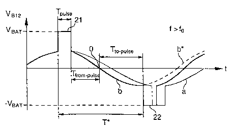
Figure 4B illustrates another case in which a variation in the conditions in
which
the vibrating device is wom has lead to an increase in the oscillation
frequency with
respect to nominal frequency fo. This results in a modification in the
movement
induced voltage frequency and thus in the voltage VB,2 across the coil
terminals. This
modification is schematically illustrated by curve b in Figure 4B. By way of
comparison, curve a of Figure 4A is also illustrated in Figure 4B.
In the situation illustrated in Figure 48, it will thus be understood that the
time
T,~ taken by the movement induced voltage to drop to a zero amplitude with
respect to its mean value is consequently reduced with respect to the
situation
illustrated in Figure 4A. Since time interval T~~,~ at the end of which the
next driving
pulse is generated, remains fixed, the driving pulse (22 in the figure) is
applied with a
slight phase error (lag) with respect to the extrema of the movement induced
voltage
as can be seen by comparing the position in time of driving pulse 22 with
respect to
curve b* which illustrates the evolution of the movement induced voltage in
the event
that no pulse is generated. From the energy point of viewi, it will be
observed,
nonetheless, that the energy balance is better than in the case where the
driving
pulses are generated periodically at fixed time intervals as in the solutions
of the prior
art.
Figure 4C illustrates the opposite case in which a variation in the conditions
in
which the vibrating device is worn has lead to a reduction in the oscillation
frequency
with respect to nominal frequency fo. This also results in a modification in
the
movement induced voltage frequency and thus in voltage VB,2 across the
terminals of
the coil which is schematically illustrated by curve c in Figure 4C. By way of
comparison, curve a of Figure 4A is also illustrated in Figure 4C.
In the situation illustrated in Figure 4C, it will thus be understood that the
time
T~",~,u~~ taken by the movement induced voltage to drop to a zero amplitude
with
respect to its mean value is consequently longer with respect to the situation
illustrated in Figure 4A. Since time interval T~p"~se at the end of which the
next driving
pulse is generated, remains fixed, the driving pulse (22 in the figure) is
applied with a
slight phase error (lead) with respect to the extrema of the movement induced
voltage
as can be seen by comparing the position in time of driving pulse 22 with
respect to
curve c* which illustrates the evolution of the movement induced voltage in
the event
that no pulse is generated. The energy balance, in this case also, is better
than in the
case where the driving pulses are generated periodically at fixed time
intervals as in
the solutions of the prior art.
CA 02431862 2003-06-05
-12-
If one compares the driving principle according to the present invention to
the
driving principle disclosed in the aforementioned European Patent Application
No.
EP 0 938 034, it will be understood that the solution according to the present
invention
is slightly less optimum from an energy point of view. Nonetheless, the
solution
according to the present invention is more robust and more stable in the sense
that
there is no risk of the vibrating device being driven at an erroneous
frequency with
respect to its real natural oscillation frequency and of the device
consequently
becoming unstable, which might arise with a vibrating device operating in
accordance
with the aforementioned European Patent Application.
The particular interest of the present invention with respect to the other
solutions of the prior art, and particularly those solutions consisting in
driving the
vibrating device at a fixed frequency, lies in the fact that the frequency at
which the
driving pulses are generated varies as a function of the conditions in which
the
vibrating device is worn by the user.
We should return to the question of the occurrence of overvoltages during
interruption of each driving pulse. The time constant of these overvoltages is
essentially determined by the characteristics of the coil, and particularly
its electrical
resistance and inductance. The appearance of each overvoltage leads to two
successive crossings, relatively close in time, of voltage VB,Z by its mean
value. These
overvoltages should thus preferably be filtered by adequate means, either at
the input
of comparator 2 by appropriate analog filtering means, or at the output of
comparator
2 by a digital filtering means, in order to prevent these mean value crossings
due to
overvoltage being detected as the desired mean value crossings, i.e. the
specific
moments which determine the time of generation of driving pulses.
In addition to the analog solution, one solution consists for example in
inhibiting
comparator 2 during a determined time interval after interruption of the
driving pulse,
such time interval being selected to be greater than the time during which the
overvoltage is produced.
According to another solution, in order to carry out °digital
filtering" of the
overvoltages, several successive samples of the signal produced at the output
of
comparator 2 should advantageously be examined. Figure 5 schematically
illustrates
voltage Vg,2 present across the coil terminals and overvoltage 40 appearing at
the end
of the generation of driving pulse 21. As schematically illustrated, the
signal is
sampled at regular intervals designated TH such that a series of signal
samples is
produced. It will be noted that the scale and the number of samples is
presented here
solely by way of example.
CA 02431862 2003-06-05
- 13-
More particularly, at the moment of overvoltage 40, four samples whose value
is less than the mean level of the movement induced voltage, are produced.
These
four samples are designated by the references 1 to 4. The sample following the
fourth
sample is higher than the mean level of the movement induced voltage.
Following the
mean level crossing of the movement induced voltage, indicated by the
reference O,
more than ten samples whose value is less than the mean value of the movement
induced voltage are generated. By way of example, the first ten samples have
been
indicated by the references 1 to 10. The situation is reversed in the case in
which one
examines an overvoltage produced at the end of a driving pulse of negative
polarity.
Thus, by examining a number N of successive samples (for example ten in the
schematic example of Figure 5) and checking that these ten successive samples
all
have a Lower value (or higher in the opposite case) than the mean level of the
movement induced voltage (in the example this mean level is zero), an
overvoltage
can be clearly distinguished from a normal mean level crossing. One should
thus
choose a number N of samples higher than the number of samples of value
inferior to
the mean level produced following an overvoltage. One should also consider the
delay
caused during determination of mean level crossing O, i.e. delay TN whose
value is
equal to N times sample period TH, and subtract this delay from time Tt~"~,~,
until
generation of the next driving pulse defined in the expression (1 )
hereinbefore, as is
schematically illustrated in Figure 5.
It will be understood that various modifrcations and/or improvements obvious
to
those skilled in the art can be made to the driving method and to the
vibrating device
described in the present description without departing from the scope of the
invention
defined by the annexed claims. In particular, it will be recalled that it is
not a priori
necessary to carry out a prior measurement of the oscillation frequency of the
vibrating device and that the time parameters defining when the driving pulses
have to
be generated, namely particularly time interval T~.~",~ can be predetermined
and fixed
to a nominal value. The prior measurement is nonetheless preferable in the
sense that
one optimises the operation of the vibrating device by being as close as
possible to
the natural frequency of the vibrating device at the moment when it is
activated.