Note : Les descriptions sont présentées dans la langue officielle dans laquelle elles ont été soumises.
CA 02432467 2008-04-09
HIGH EFFICIENCY INTERDIGITAL FILTER
BACKGROUND OF THE INVENTION
Statement of the Technical Field
The inventive arrangements relate generally to methods and
apparatus for providing increased design flexibility for RF circuits, and more
particularly for optimization of dielectric circuit board materials for
improved
performance in filters having two ports and coupled resonant lines.
Description of the Related Art
RF circuits, transmission lines and antenna elements are commonly
manufactured on specially designed substrate boards. For the purposes of these
types of circuits, it is important to maintain careful control over impedance
characteristics. If the impedance of different parts of the circuit do not
match,
this can result in inefficient power transfer, unnecessary heating of
components,
and other problems. Electrical length of transmission lines and radiators in
these
circuits can also be a critical design factor.
Two critical factors affecting the performance of a substrate
material are permittivity (sometimes called the relative permittivity or E,)
and the
loss tangent (sometimes referred to as the dissipation factor). The relative
permittivity determines the speed of the signal, and therefore the electrical
iength of transmission lines and other components implemented on the
substrate. The loss tangent characterizes the amount of loss that occurs for
signals traversing the substrate material. Losses tend to increase with
increases
in frequency. Accordingly, low loss materials become even more important with
increasing frequency, particularly when designing receiver front ends and low
noise amplifier circuits.
Printed transmission lines, passive circuits and radiating elements
used in RF circuits are typically formed in one of three ways. One
configuration
known as microstrip, places the signal line on a board surface and provides a
-1-
CA 02432467 2003-06-19
second conductive layer, commonly referred to as a ground plane. A second
type of configuration known as buried microstrip is similar except that the
signal
line is covered with a dielectric substrate material. In a third configuration
known as stripline, the signal line is sandwiched between two electrically
conductive (ground) planes. Ignoring loss, the characteristic irnpedance of a
transmission line, such as stripline or microstrip, is equal to 'TvC, where LI
is
the inductance per unit length and C, is the capacitance per unit length. The
values of L, and C, are generally determined by the physical geometry and
spacing of the line structure as well as the permittivity of the dielectric
material(s) used to separate the transmission line structures. Conventional
substrate materials typically have a relative permeability of approximately
1Ø
In conventional RF design, a substrate material is selected that has
a relative permittivity value suitable for the design. Once the substrate
material
is selected, the line characteristic impedance value is exclusively adjusted
by
controlling the line geometry and physical structure.
Radio frequency (RF) circuits are typically embodied in hybrid
circuits in which a plurality of active and passive circuit components are
mounted and connected together on a surface of an electrically insulating
board
substrate such as a ceramic substrate. The various components are generally
interconnected by printed metallic conductors of copper, gold, or tantalum,
for
example that are transmission lines as stripline or microstrip or twin-line
structures.
The permittivity of the chosen substrate material for a
transmission line, passive RF device, or radiating element determines the
physical wavelength of RF energy at a given frequency for that line structure.
One problem encountered when designing microelectronic RF circuitry is the
selection of a dielectric board substrate material that is optimized for all
of the
various passive components, radiating elements and transmission line circuits
to
be formed on the board. In particular, the geometry of certain circuit
elements
may be physically large or miniaturized due to the unique electriical or
impedance
characteristics required for such elements. For example, many circuit elements
-2-
CA 02432467 2003-06-19
or tuned circuits may need to be an electrical 1/4 wave. Similarly, the line
widths required for exceptionally high or low characteristic impedance values
can, in many instances, be too narrow or too wide respectively for practical
implementation for a given substrate. Since the physical size of the
microstrip or
stripline is inversely related to the relative permittivity of the dielectric
material,
the dimensions of a transmission line can be affected greatly by the choice of
substrate board material.
Still, an optimal board substrate material design choice for some
components may be inconsistent with the optimal board substrate material for
other components, such as antenna elements or filters. Moreover, some design
objectives for a circuit component may be inconsistent with one another. For
example, it may be desirable to reduce the size of an antenna element. This
could be accomplished by selecting a board material with a relatively high
dielectric. However, the use of a dielectric with a higher relative
permittivity will
generally have the undesired effect of reducing the radiation efficiency of
the
antenna. Accordingly, the constraints of a circuit board substrate having
selected relative dielectric properties often results in design compromises
that
can negatively affect the electrical performance and/or physical
characteristics of
the overall circuit.
An inherent problem with the foregoing approach is that, at least
with respect to the substrate material, the only control variable for line
impedance is the relative permittivity, e,.. This limitation highlights an
important
problem with conventional substrate materials, i.e. they fail to take
advantage of
the other factor that determines characteristic impedance, namely Ll , the
inductance per unit length of the transmission line.
Yet another problem that is encountered in RF circuit design is the
optimization of circuit components for operation on different RF frequency
bands. Line impedances and lengths that are optimized for a first RF frequency
band may provide inferior performance when used for other bands, either due to
impedance variations and/or variations in electrical length. Such limitations
can
limit the effective operational frequency range for a given RF system.
-3-
CA 02432467 2003-06-19
Conventional circuit board substrates are generally formed by
processes such as casting or spray coating which generally result in uniform
substrate physical properties, including the permittivity. Accordingly,
conventional dielectric substrate arrangements for RF circuits have proven to
be
a limitation in designing circuits that are optimal in regards to both
electrical and
physical size characteristics.
SUMMARY OF THE INVENTION
In a first embodiment according to the invention, a circuit for
processing radio frequency signals comprises a substrate where the circuit can
be placed. The substrate includes at least one dielectric layer having a first
set
of substrate properties over a first region and at least a second set of
substrate
properties over a second region. The second set of substrate properties can be
different than the first set of substrate properties. The circuit further
comprises
at least one ground plane coupled to the substrate and a interdigital filter
having
a plurality of resonator elements with at least a portion of alternating
adjacent
ends of the plurality of resonator elements coupled to the at least one ground
plane and at least a portion of the interdigital filter coupled to the second
region.
In a second embodiment according to the invention, a printed
circuit for processing radio frequency signals comprises a substrate upon
which
the circuit can be placed. The substrate includes at least one dielectric
layer
having a first set of dielectric and magnetic properties over a first region
and at
least a second set of dielectric and magnetic properties over a second region.
The second set of dielectric and magnetic properties provide a different
dielectric
permittivity and magnetic permeability as compared to the first set of
dielectric
properties. The printed circuit further comprises at least one ground disposed
in
or on the substrate and an interdigital filter. The iriterdigital filter
includes a
plurality of resonator elements with at least a portion of alternating
adjacent
ends of the plurality of resonator elements coupled to the at least one ground
plane and at least a portion of the interdigital filter coupled to the second
region.
-4-
CA 02432467 2003-06-19
In a third embodiment of the present invention, a printed circuit for
processing radio frequency signals comprises a substrate including substrate
regions upon which the circuit can be placed. The circuit is an interdigital
filter
including a plurality of resonator line elements and at least one ground
coupled
to said substrate. The plurality of resonator line elements are at least
partially
coupled to respective substrate regions that have substrate characteristics
that
are each independently customizable
BRIEF DESCRIPTION OF THE DRAWINGS
Fig. 1 is a top view of an interdigital filter formed on a substrate
for reducing the size of the interdigital filter in accordance with the
present
invention.
Fig. 2 is a cross-sectional view of the interdigital filter of Fig. 1
taken along line A-A.
Fig. 3 is a cross-sectional view of an alternate embodiment of the
interdigital filter of Fig. 1 taken along line A-A in accordance with the
present
invention
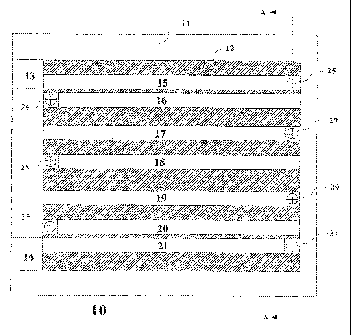
Fig. 4 is a cross-sectional view of another alternate embodiment of
the interdigital filter of Fig. 1 taken along line A-A.
Fig. 5 is a flow chart that is useful for illustrating a process for
manufacturing an interdigital filter of reduced physical size in accordance
with
the present invention.
DETAILED DESCRIPTION OF THE PREFERRED EMBODIMENTS
Referring to Fig. 1, interdigital filter 10 serving as an interdigital
bandpass filter is mounted on layer of substrate material or dielectric
material
(dielectric layer) 11. It should be understood that the present invention and
the
interdigital structure is not necessarily limited to a bandpass filter. In
Fig. 1, the
interdigital filter 10 is configured as having an input port 13 and an output
port
14 and a plurality (11 through n) of mutually coupled resonator elements 15,
16,
17, 18, 19, 20, and 21 . Resonator elements 15 and 21 are also considered
-5-
CA 02432467 2003-06-19
terminating lines. Although seven resonators are shown, it should be
understood that more or less resonator elements could be used in accordance
with the present invention. The interdigital bandpass filter preferably
consists of
mutually coupled resonators which can be physically less than a quarter
wavelength long and which can be grounded at one end (as shown by ground
points 25, 26, 27, 28, 29, 30, and 31) and capacitively loaded at an opposing
end of the resonator element. The ground points are typically grounded to a
ground plane 50 through metalized vias 35 as shown in the cross-sectional view
of FIG. 2. The interdigital structure is formed by grounding the resonator
elements on alternating ends as opposed to adjacent ends as found in a typical
combline filter. The present invention utilizes substrate materials of
differing
substrate characteristics coupled to the resonator elements. In particular,
substrate materials (12 and 40) having different dielectric properties and
magnetic properties are coupled beneath and between each resonator in the
plurality of resonators 15-21. FIG. 2 depicts a cross-sectional view of the
interdigital filter 10 along line A-A, where magnetic materials 40 are placed
underneath the resonators (15-21) to shorten and widen the lines of the
filter.
Magnetic materials between the lines and ground provide an additional means to
control the width of the line. FIG. 2 further illustrates that where high
coupling
is desired (close spacing), the coupling can be improved (i.e., the even and
odd
mode impedances better matched).
Generally, interdigital filter structures have a plurality of resonator
elements that are a quarter-wavelength long at the midband frequency and is
short-circuited at one end and open-circuited at an opposing end. Coupling is
achieved by way of the fields fringing between adjacent resonator elements. In
the embodiment of FIG. 1, elements 16-20 serve as resonators and elements 15
and 21 operate as impedance transforming sections. FIG. 3 illustrates an cross-
sectional view along line A-A of an alternative embodiment of the present
invention, where the only distinction between the embodiment of FIG. 2 and
FIG. 3 is that the resonator elements or terminating lines 15 and 21 are open-
circuited rather than being short-circuited line elements (to ground). In this
-6-
_.
CA 02432467 2003-06-19
embodiment, all of the resonator elements including the terminating lines 15
and
21 serve as resonators. Thus, the embodiment of FIG. 3 will provide a wider
bandwidth interdigital filter than the embodiment of FIG. 2 (where the
terminating element s 15 and 21 are short-circuited to ground.
The internal line spacings between resonators can be sufficiently
large to avoid any tolerance problems, even for moderately wide bandwidths.
Bandwidth is a design constraint and traded against fabrication constraints.
Resonator length is also a design choice, except that it must be less than 90
degrees, as at 90 degrees length, the magnetic and electrostatic coupling
totally
cancel. At less than 90 degrees, magnetic coupling predominates. Tight
coupling occurs at 90 degrees resonator length even for moderately wide
spacings. Because the lines are ideally resonant length, loading capacitance
is
not typically required. Although the interdigital structure is not as compact
as a
similar combline structure, the resonator unloaded Q is higher. The higher
unloaded Q makes the interdigital structure particularly well suited when low
insertion loss is required. The high unloaded Q is also an advantage in the
design of very narrow band filters, except the absence of loading caps
dictates
either extremeiy tight tolerance or siight loading for tuning purposes. The
excellent coupiing properties make the interdigital suitable for bandwidth
applications of up to 70%.
FIG. 4 is a cross-sectional view of FIG. 1 along line A-A illustrating
another alternative embodiment where the differing substrate materials 12 and
40 are coupled between the top plane of the substrate 11 and the ground plane
50. In particular, substrate material 40 couples between the resonator lines
or
traces and the ground plane 50. It will be appreciated by those skilled in the
art,
however, that the invention is not so limited and the coupled lines also can
be
configured in differing shapes based on the desired function and the
properties
of substrate materials coupled thereto.
As previously discussed above, the e{ements 15 through 21 can
be resonant lines. A resonant line is a transmission line typically used in
radio
frequency (RF) circuits. A resonant line has finite length and is not
terminated in
-7-
CA 02432467 2003-06-19
its characteristic impedance (Zo). The mismatch between Zo and the impedance
at the termination (load impedance, ZL) causes energy reflections. These
energy
reflections can increase or decrease a voltage on the line, depending on the
frequency of the applied voltage and the position on the line where the
voltage is
being measured. Accordingly, at some frequencies a resonant line of a given
length may have high input impedance, similar to a parallel resonant circuit
at
resonance, while at other frequencies the resonant line may have low input
impedance, similar to a series resonant circuit at resonance. At other
frequencies the resonant line may also have complex or reactive impedances.
On printed circuit boards or substrates, single port resonant lines
are typically implemented by creating a line with a single port at the input
and
either open-circuited or short-circuited to ground at the termination. The
electrical length of a single port resonant line is usually some multiple of a
quarter-wavelength of a selected frequency. On a short-circuited line, each
point
at an odd number of quarter-wavelengths from the termination has high
impedance and relative voltage maxima, and each point at an even number of
quarter-wavelengths from the termination has a low impedance and a relative
voltage minima. The positions of voltage maxima and minima are reversed on an
open-circuited resonant line. The input impedance to a single port resonant
line
is typically resistive when the length of the resonant line is an even or odd
multiple of the quarter-wavelength of the operatiorial frequency. That is, the
input to the single port resonant line is at a position of voltage maxima or
minima.
When the input to the single port resonant line is at a position
between the voltage maxima and minima points, the input impedance can have
reactive components, which can be a useful feature. For example, resonant
lines may also act as nearly pure capacitances or inductances. For example, an
open-circuited line acts as a pure capacitance at 1/8 wavelength long, acts as
a
series LC impedance at 1/4 wavelength long, acts a pure inductance at 3/8
wavelengths long, and acts like a parallel LC circuit at 1/2 wavelength long.
This cycle repeats every half wavelength with smooth transitions between each
-8-
CA 02432467 2003-06-19
of the above mentioned points. Thus, properly chosen single port resonant line
segments may be used as parallel-resonant, series-resonant, iriductive, or
capacitive circuits.
A short-circuited line acts as a pure inductance at 1/8 wavelength
long, acts as a parallel LC impedance at 1/4 wavelength long, acts a pure
capacitance at 3/8 wavelengths long, and acts like a series LC circuit at 1/2
wavelength long. This cycle repeats every half wavelength with smooth
transitions between each of the above mentioned points. Thus, properly chosen
single port resonant line segments may be used as parallel-resonant, series-
resonant, inductive, or capacitive circuits.
When a resonant line is terminated in capacitance, the capacitor
does not absorb energy, but returns all of the energy to the circuit. The
impedance discontinuity between the line impedance and the termination
produce a reflected wave that adds to the incident wave to produce a standing
wave. The standing wave voltage is a minimum at a distance of exactly 1/8
wavelength from the end if the termination when the termination capacitive
reactance has the same absolute value as Zo. If the capacitive reactance is
greater than Zo (smaller capacitance), the termination looks more like an open
circuit and the voltage minimum moves away from the end. If the capacitive
reactance is smaller than Zo, the voltage minimum moves closer to the end.
Single port resonant lines are commonly manufactured on specially
designed printed circuit boards. The resonant lines can be formed many
different ways. Three common configurations are described next. One
configuration known as microstrip places the resonant line on a board surface
and provides a second conductive layer coupled to the board. This second
conductive layer is commonly referred to as a ground plane. A second type of
configuration known as buried microstrip is similar except that the resonant
line
is covered with a dielectric substrate material. In a third configuration
known as
stripline, the resonant line is sandwiched between two electrically conductive
(ground) planes, which can be proximate to the board or coupled to the board.
-9-
CA 02432467 2003-06-19
As defined herein, coupled to the board means attached to the surface of the
board or contained within the board.
Low dielectric constant printed circuit board materials are
ordinarily selected for RF circuit designs. For example,
polytetrafluoroethylene
(PTFE) based composites such as RT/duroid 6002 (dielectric constant of 2.94;
loss tangent of .009) and RT/duroid 5880 (dielectric constant of 2.2; loss
tangent of .0007) are both available from Rogers Microwave Products,
Advanced Circuit Materials Division, 100 S. Roosevelt Ave, Chandler, AZ
85226. Both of these materials are common board material choices. The above
board materials provide dielectric layers having relatively low dielectric
constants
with accompanying low loss tangents.
However, use of conventional board materials can compromise the
miniaturization of circuit elements and may also compromise some performance
aspects of circuits that can benefit from high dielectric constant layers. A
typical tradeoff in a communications circuit is between the physical size of
antenna elements versus efficiency. By comparison, the present invention
provides the circuit designer with an added level of flexibility by permitting
use
of locally high dielectric constant dielectric layer portions and locally low
dielectric constant layer portions. In addition, iocaiized board portions can
be
optimized for efficiency through the ability to select localized magnetic
board
properties. This added flexibility enables improved performance and line
element
density not otherwise possible.
Dielectric substrate boards having metamaterial portions providing
localized and selectable magnetic and dielectric properties can be prepared in
the
following manner. As defined herein, the term "metamaterials" refers to
composite materials formed from the mixing or arrangement of two or more
different materials at a very fine level, such as the Angstrom or nanometer
level.
Metamaterials allow tailoring of electromagnetic properties of the composite,
which can be defined by effective electromagnetic parameters comprising
effective electrical permittivity (or dielectric constant) and the effective
magnetic
permeability.
-10-
CA 02432467 2003-06-19
Appropriate bulk dielectric substrate materials can be obtained
from commercial materials manufacturers, such as DuPont and Ferro. The
unprocessed material, commonly called Green Tape', can be cut into sized
portions from a bulk dielectric tape, such as into 6 inch by 6 inch portions.
For
example, DuPont Microcircuit Materials provides Green Tape material systems,
such as 951 Low-Temperature Cofire Dielectric T'ape and Ferro Electronic
Materials ULF28-30 Ultra Low Fire COG dielectric: formulation. These substrate
materials can be used to provide dielectric layers having relatively moderate
dielectric constants with accompanying relatively low loss tangents for
circuit
operation at microwave frequencies once fired.
In the process of creating a microwave circuit using multiple
sheets of dielectric substrate material, features such as vias, voids, holes,
or
cavities can be punched through one or more layers of tape. Voids can be
defined using mechanical means (e.g. punch) or directed energy means (e.g.,
laser drilling, photolithography), but voids can also be defined using any
other
suitable method. Some vias can reach through the entire thickness of the sized
substrate, while some voids can reach only through varying portions of the
substrate thickness.
The vias can then be filled with metal or other dielectric or
magnetic materials, or mixtures thereof, usually using stencils for precise
placement of the backfill materials. The individual layers of tape can be
stacked
together in a conventional process to produce a complete, multi-layer
substrate.
Alternatively, individual layers of tape can be stacked together to produce an
incomplete, multi-layer substrate generally referred to as a sub-stack.
Voided regions can also remain voids. If backfilled with selected
materials, the selected materials preferably include metamaterials. The choice
of
a metamaterial composition can provide controllable effective dielectric
constants over a relatively continuous range from less than 2 to at least
2650.
Controllable magnetic properties are also available from certain
metamaterials.
For example, through choice of suitable materials the relative effective
magnetic
permeability generally can range from about 4 to 116 for most practical RF
-11-
CA 02432467 2003-06-19
applications. However, the relative effective magnetic permeability can be as
low
as about 2 or reach into the thousands.
The term "differentially modified" as used herein refers to
modifications, including dopants, to a dielectric substrate layer that result
in at
least one of the dielectric and magnetic properties being different at one
portion
of the substrate as compared to another portion. A differentially modified
board
substrate preferably includes one or more metamaterial containing regions.
For example, the modification can be selective modification where
certain dielectric layer portions are modified to produce a first set of
dielectric or
magnetic properties, while other dielectric layer portions are modified
differentially or left unmodified to provide dielectric and/or magnetic
properties
different from the first set of properties. Differential modification can be
accomplished in a variety of different ways.
According to one embodiment, a supplemental dielectric layer can
be added to the dielectric layer. Techniques known in the art such as various
spray technologies, spin-on technologies, various deposition technologies or
sputtering can be used to apply the supplemental dielectric layer. The
supplemental dielectric layer can be selectively added in localized regions,
including inside voids or holes, or over the entire existing dielectric layer.
For
example, a supplemental dielectric layer can be used for providing a substrate
portion having an increased effective dielectric constant.
Responses of a dielectric layer to a given energetic stimuli may be
substantially permanent in whole or in part. Permanent responses permit one
time application of an appropriate stimulus to achieve one or more desired
physical dielectric layer properties. Physical properties may also be
dynamically
controlled, such as through the use of discharge electrodes which can permit
application of a time-varying electrical field across the dielectric layer.
Dynamic
control of the dielectric layer properties, such as the dielectric constant,
can be
used to retune the dielectric layer physical characteristics to optimize the
performance of the resonant line in response to varying signal
characteristics, for
example a substantial change in operating frequency.
-12-
CA 02432467 2003-06-19
The differential modifying step can further include locally adding
additional material to the dielectric layer or supplemental dielectric layer.
The
addition of material can be used to further control the effective dielectric
constant or magnetic properties of the dielectric layer to achiE:ve a given
design
objective.
The additional material can include a plurality of metallic and/or
ceramic particles. Metal particles preferably include iron, tungsten, cobalt,
vanadium, manganese, certain rare-earth metals, nickel or niobium particles.
The particles are preferably nanometer size particles, generally having sub-
micron physical dimensions, hereafter referred to as nanoparticles.
The particles, such as nanoparticles, can preferably be
organofunctionalized composite particles. For example, organofunctionalized
composite particles can include particles having metallic cores with
electrically
insulating coatings or electrically insulating cores with a metallic coating.
Magnetic metamaterial particles that are generally suitable for
controlling magnetic properties of dielectric layer for a variety of
applications
described herein include ferrite organoceramics (FexCyHz)-(Ca/Sr/Ba-Ceramic).
These particles work well for applications in the frequency range of 8-40 GHz.
Alternatively, or in addition thereto, niobium organoceramics (NbCyHz)-
(Ca/Sr/Ba-Ceramic) are useful for the frequency range of 12-40 GHz. The
materials designated for high frequency are also applicable to low frequency
applications. These and other types of composite particles can be obtained
commercially.
In general, coated particles are preferable for use with the present
invention as they can aid in binding with a polymer matrix or side chain
moiety.
In addition to controlling the magnetic properties of the dielectric, the
added
particles can also be used to control the effective dielectric constant of the
material. Using a fill ratio of composite particles from approximately 1 to
70%,
it is possible to raise and possibly lower the dielectric constant of
substrate
dielectric layer and/or supplemental dielectric layer portions sigriificantly.
For
-13-
CA 02432467 2003-06-19
example, adding organofunctionalized nanoparticVes to a dielectric layer can
be
used to raise the dielectric constant of the modified dielectric layer
portions.
Particles can be applied by a variety of techniques including
polyblending, mixing and filling with agitation. For example, if the
dielectric
layer includes a polymer, the dielectric constant may be raisec9 from a
nominal
value of 2 to as high as 10 by using a variety of particles with a fill ratio
of up to
about 70%.
Metal oxides useful for this purpose can include aluminum oxide,
calcium oxide, magnesium oxide, nickel oxide, zirconium oxide and niobium (11,
IV and V) oxide. Lithium niobate {LiNb03), and zirconates, such as calcium
zirconate and magnesium zirconate, also may be used.
The selectable dielectric properties can be localized to areas as
small as about 10 nanometers, or cover large area regions, including the
entire
board substrate surface. Conventional techniques such as lithography and
etching along with deposition processing can be used for localized dielectric
and
magnetic property manipulation.
Materials can be prepared mixed with other materials or including
varying densities of voided regions (which generally introduce air) to produce
effective dielectric constants in a substantially continuous range from 2 to
about
2650, as well as other potentially desired substrate properties. For example,
materials exhibiting a low dielectric constant (< 2 to about 4) include silica
with
varying densities of voided regions. Alumina with varying densities of voided
regions can provide a dielectric constant of about 4 to 9. Neither silica nor
alumina have any significant magnetic permeability. However, magnetic
particles can be added, such as up to 20 wt. %, to render these or any other
material significantly magnetic. For example, magnetic properties may be
tailored with organofunctionality. The impact on dielectric constant from
adding
magnetic materials generally results in an increase in the dielectric
constant.
Medium dielectric constant materials have a dielectric constant
generally in the range of 70 to 500 +/- 10%. As noted above these materials
may be mixed with other materials or voids to provide desired effective
dielectric
-14-
CA 02432467 2003-06-19
constant values. These materials can include ferrite doped calcium titanate.
Doping metals can include magnesium, strontium and niobium. These materials
have a range of 45 to 600 in relative magnetic permeability.
For high dielectric constant appiications, ferrite or niobium doped
calcium or barium titanate zirconates can be used. These materials have a
dielectric constant of about 2200 to 2650. Doping percentages for these
materials are generally from about 1 to 10 %. As noted with respect to other
materials, these materials may be mixed with other materials or voids to
provide
desired effective dielectric constant values.
These materials can generally be modified through various
molecular modification processing. Modification processing can include void
creation followed by filling with materials such as carbon and fluorine based
organo functional materials, such as polytetrafluoroethylene PTFE.
Alternatively or in addition to organofunctional integration,
processing can include solid freeform fabrication (SFF), photo, uv, x-ray, e-
beam
or ion-beam irradiation. Lithography can also be performed using photo, uv, x-
ray, e-beam or ion-beam radiation.
Different materials, including metamaterials, can be applied to
different areas on substrate layers (sub-stacks), so that a plurality of areas
of the
substrate layers (sub-stacks) have different dielectric and/or magnetic
properties.
The backfill materials, such as noted above, may be used in conjunction with
one or more additional processing steps to attain desired, dielectric and/or
magnetic properties, either locally or over a bulk substrate portion.
A top layer conductor print is then generally applied to the
modified substrate layer, sub-stack, or complete stack. Conductor traces can
be
provided using thin film techniques, thick film techniques, electroplating or
any
other suitable technique. The processes used to define the conductor pattern
include, but are not limited to standard lithography and stencil.
A base plate is then generally obtained for collating and aiigning a
plurality of modified board substrates. Alignment holes through each of the
plurality of substrate boards can be used for this purpose.
-15-
CA 02432467 2003-06-19
The plurality of layers of substrate, one or more sub-stacks, or
combination of layers and sub-stacks can then be laminated (e.g. mechanically
pressed) together using either isostatic pressure, which puts pressure on the
material from all directions, or uniaxial pressure, which puts pressure on the
material from only one direction. The laminate substrate is then is further
processed as described above or placed into an oven to be fired to a
temperature
suitable for the processed substrate (approximately 850 C to 900 C for the
materials cited above).
The plurality of ceramic tape layers and stacked sub-stacks of
substrates can then be fired, using a suitable furnace that can be controlled
to
rise in temperature at a rate suitable for the substrate materials used. The
process conditions used, such as the rate of increase in temperature, final
temperature, cool down profile, and any necessary holds, are selected mindful
of
the substrate material and any material backfilled therein or deposited
thereon.
Following firing, stacked substrate boards, typically, are inspected for flaws
using an optical microscope.
The stacked ceramic substrates can then be optionally diced into
cingulated pieces as small as required to meet circuit functional
requirements.
Following final inspection, the cingulated substrate pieces can then be
mounted
to a test fixture for evaluation of their various characteristics, such as to
assure
that the dielectric, magnetic and/or electrical characteristics are within
specified
limits.
Thus, dielectric substrate materials can be provided with localized
tunable dielectric and/or magnetic characteristics for improving the density
and
performance of circuits including those having coupled lines serving as
bandpass
filters. The dielectric flexibility allows independent optimization of the
line
impedance and electromagnetic coupling of the various elements comprising the
interdigital filter.
However, use of conventional board materials can compromise the
miniaturization of circuit elements and may also compromise some performance
aspects of circuits that can benefit from high dielectric constant layers. A
-16-
CA 02432467 2003-06-19
typical tradeoff in a communications circuit is between the physical size of a
resonant line versus operational frequency. By comparison, the present
invention provides the circuit designer with an added level of flexibility by
permitting use of a high dielectric constant dielectric layer portion with
magnetic
properties optimized for reducing the size of a resonant line and/or
transformer
line for operation at a specific frequency. Further, the present invention
also
provides the circuit designer with means for controlling the quality factor
(Q) of
the resonant line aspects of the two port line. This added flexibility enables
improved performance and resonant line density and performance not otherwise
possible for radio frequency circuits (RF). As defined herein, radio frequency
means any frequency that can be used to propagate an electromagnetic wave.
Referring once again to FIGs. 1 and 2, the interdigital filter is
mounted on a substrate or layer of dielectric material (dielectric layer) 11
that
includes at least a first region 9 having a first set of substrate properties
(such
as dielectric properties) including a first dielectric constant, and at least
a second
region 12 having a second set of substrate properties including a second
dielectric constant. The first dielectric constant is preferably different
from the
second dielectric constant. In this instance, the second region 12 can lie
between the resonator line sections 15-21. The substrate can also have other
regions such as region 40 having yet another set of substrate properties. As
shown, the region 40 occupies an area between the respective resonator
elements and the ground plane 50. The present invention contemplates that
each of the regions 9, 12 and 40 can have their own dielectric properties, but
two out of the three regions could also have substrate properties that are
equivalent as contemplated by the present invention.
The dielectric constant of the regions 12 and/or 40 can have a
higher permittivity and/or permeability than the first region 9. Accordingly,
the
size of the resonator elements 15-21 (or transformer elements 15 and 21 as the
case may be in the embodiment of FIG. 1) can be smaller than would otherwise
be necessary to achieve a selected capacitance between the respective
resonator elements and the ground plane 50. Accordingly, this allows for the
-17-
CA 02432467 2003-06-19
area of the substrate 11 incorporating the interdigital filter to be smaller
than the
area that would be required on a conventional circuit board.
The propagation velocity of a signal traveling ori a resonant line
approximately inversely proportional to . Accordingly, increasing the
permeability and/or permittivity in the regions 12 or 40 decreases propagation
velocity of the signal on the resonant lines, and thus the signal wavelength.
Hence, the one-quarter wavelength (or any multiple thereof) of the line can be
reduced by increasing the permeability and/or permittivity. Accordingly, the
area
of the dielectric layer or substrate 11 incorporating the interdigital filter
can be
smalfer than the area required on a conventional circuit board.
The regions 12 and 40 also can have a permittivity selected to
achieve a particular capacitance for portions or all of a resonator line.
Further,
the permeability can be selected to result in a particular inductance for a
particular resonator element as well. The permittivity and perrneability can
be
chosen to result in a desired Zo or other filter characteristics. Zo can be
selected
to achieve a desired Q for particular resonances on the resonant line
portions,
shape the resonant response of the filter, and/or adjust voltage maxima and
minima. Further, Zo can be selected to suppress higher resonant modes and/or
to create a mismatch between the impedance of the interdigital filter and the
impedance of free space. This impedance mismatch can help to minimize RF
radiation from the interdigital filter and reduce electromagnetic interference
(EMI).
The resonant characteristics of the interdigital filter 10 can be
distributed through the first and second regions (or other regions) of the
substrate as the electric fields and magnetic fields formed in these regions
store
and release energy. The amount of energy stored and released by the fields can
be adjusted by controlling permittivities and permeabilities associated with
different regions in the dielectric layer. For example, a higher permittivity
in a
particular region will result in greater energy stored in the electric fields
formed
in that region. Likewise, higher permeability in a particular region will
result in
greater energy stored in the magnetic fields formed in that region.
-18-
CA 02432467 2003-06-19
Because the size of the resonant elements or lines can generally be
smaller than those on a conventional circuit board, the capacitance can be
more
easily adjusted to locate voltage minimums and maximums at desired locations
along the interdigital filter. Further, regions where the resonant line acts
like an
inductance or a capacitance can be more easily controlled as well. Hence, the
present invention enables greater configurability of resonant lines in
comparison
to prior art.
In one embodiment of the invention the permeability of the board
substrate dielectric layer can be controlled by the addition of ferromagnetic,
diamagnetic or paramagnetic material into the second region(s) to increase the
inductance of portions of the interdigital filter. Preferably, the
conductivity of
the ferromagnetic material is low so as to minimize loss and not short-circuit
the
resonator sections to any other lines in or on the dielectric layer or to the
ground
plane.
It should be noted that the interdigital filter configurations are not
limited to the exemplary figures shown. For example, the interdigital filters
can
have resonator elements with varying shapes and can be positioned to have
varying distances between the resonator elements line and the ground plane or
circuit layer surface. Further, any number of dielectric, ferromagnetic,
diamagnetic and/or paramagnetic materials can be incorporated into any regions
of the substrate. In one embodiment, Zo can be controlled over the entire
length
of interdigital filter, or any part thereof, using multiple dielectric and
magnetic
mixtures or concentrations to vary Zo over different regions of the line. For
example, Zo can be controlled to minimize radiation of RF energy or
electromagnetic interference (EMI) from the interdigital filter. Further, the
dielectric and magnetic properties can be differentially modified at selected
portions of the dielectric layer to optimize resonant line performance. In yet
another arrangement all dielectric layer portions can be modified by
differentially
modifying dielectric properties and magnetic properties in all regions of the
dielectric layer.
-19-
CA 02432467 2003-06-19
The term 'differential modifying" as used hereir- refers to any
modifications, including additions, to the dielectric layer that result in at
least
one of the dielectric and magnetic properties being different at one portion
of the
substrate as compared to another portion. For example, the modification can be
selective modification where certain dielectric layer portions are modified to
produce a first set of dielectric or magnetic properties, while other
dielectric
layer portions are left un-modified having dielectric and magnetic properties
different from the first set of properties resulting from the modification.
An embodiment of the method for providing a size and
performance optimized resonant line is described with reference to the text
below and the flow chart presented in Fig. 56. Referring to Fig. 56, in step
510,
board dielectric material is prepared for modification. The board material can
include commercially available off the shelf board material, such as RT/duroid
6002, or customized board material formed from a polymer material, or some
combination thereof. The preparation process cari be made dependent upon the
type of board material selected.
In step 520, one or more dielectric layer portions such as the first
region 9 or second region 12 is differentially modified so that the dielectric
constant or magnetic properties in the second portion 12 is different as
compared to dielectric constant or magnetic properties of the first region 9.
In
step 530, a metal layer is applied to form the interdigital filter. In step
520,
differential modification can be accomplished in several different ways.
According to one embodiment, a supplemental dielectric layer can
be added to dielectric layer 11. Techniques known in the art such as various
spray technologies, spin-on technoiogies, various deposition technologies or
sputtering can be used to apply the supplemental layer. The supplemental layer
can be selectively added in the region 12 or 40, or over the entire existing
dielectric layer 11.
The differential modifying step 520 can further include adding
additional material to the dielectric layer 11. The addition of material can
be
used to further control dielectric constant or magnetic properties of the
dielectric
-20-
CA 02432467 2003-06-19
layer 11 to improve resonant line efficiency or achieve a specific resonant
line
size.
The additional material that can be added to the dielectric layer
can include a plurality of particles. The particles are preferably metallic
and/or
ceramic particles. Metal particles preferably include iron, tungsten, cobalt,
vanadium, manganese, certain rare-earth metals, nickel or niobium particles.
The particles are preferably nanosize particles, generally having sub-micron
physical dimensions, hereafter referred to as nanoparticles.
The particles, such as nanoparticles, can preferably be
organofunctionalized composite particles. For example, organofunctionalized
composite particles can include particles having metallic cores with
electrically
insulating coatings or electrically insulating cores with a metallic coatings.
Candidate magnetic meta-material particles that are particularly
suitable for controlling magnetic properties of dielectric layer 11 for the
resonant
line applications described herein include Ferrite organoceramics (FexCyHz)-
(Ca/Sr/Ba-Ceramic). These particles work well for frequencies in the range of
8-
40GHz. Alternatively, or in addition thereto, Niobium organoceramics (NbCyHz)-
(Ca/Sr/Ba-Ceramic) are particularly useful for the frequency range of 1 2-
40GHz.
These and other types of composite particles can be obtained commercially.
In general, coated particles are preferable for use with the present
invention as they can aid in binding with a polymer matrix or side chain
moiety.
In addition to controlling the magnetic properties of the dielectric layer 11,
the
added particles can also be used to control dielectric constant of the
material.
Using a fill ratio of composite particles from approximately 1 to 70%, it is
possible to raise and possibly lower, the dielectric constant of substrate
dielectric layer and/or supplemental dielectric layer portions sigriificantly.
For
example, adding organofunctionalized nanoparticles to a dielectric layer can
be
used to raise the dielectric constant of the modified dielectric layer
portions.
Particles can be applied by a variety of techniques including
polyblending, mixing and filling with agitation. For example, if the
dielectric
layer includes a polymer, the dielectric constant may be raised from a nominal
-21-
CA 02432467 2003-06-19
value of 2 to as high as 10 by using a variety of particles with a fill ratio
of up to
70%.
Metal oxides useful for this purpose can include aluminum oxide,
calcium oxide, magnesium oxide, nickel oxide, zirconium oxide and niobium (II,
IV and V) oxide. Lithium niobate (LiNbOa), and zirconates, such as calcium
zirconate and magnesium zirconate, also may be used.
Whife the preferred embodiments of the invention have been
illustrated and described, it will be clear that the invention is not so
limited.
Numerous modifications, changes, variations, substitutions and equivalents
will
occur to those skilled in the art without departing from the spirit and scope
of
the present invention as described in the claims.
-22-