Note : Les descriptions sont présentées dans la langue officielle dans laquelle elles ont été soumises.
CA 02437243 2003-08-14
-1-
FLEXIBLE SURFACE LAYER FILM FOR DELIVERY OF
HIGHLY FILLED OR LOW CROSS-LINKED THERMALLY
CONDUCTIVE INTERFACE PADS
BACKGROIJND OF THE INVENTION
The present invention relates generallv to an
improved composite material for use as an interface or in
fcrminq a mounting pad to be interposed along a::eat.
dissipating path between a solid state electronic device
and a heat sinking surface. The composite consists of a
mu~ti -layer pad flanked by skin layers which may be
different in chemical composition and/or physical
properties integrally bonded to and mated with the bulk
laver so as to form a composite having good mechanical
properties along with excellent thermal properties. The
composites of the present invention are useful in the
production and manufacturing of electronic systems
inasmuch as the skin layers are well adapted to receive
and reasonably hold a release liner, which is readily
removable from the composite during or following
production and handling operations.
In order to enhance the thermal properties of
iriterface mounting pads, it is generally the practice to
increase the particulate loading of the resin system of a
composite. Increased loading, while improving the
thermal properties, generally has an adverse effect upon
the mechanical properties. To decrease hardness of
highly filled composites, it is customary to reduce
cross-linking of the resin system or use gel-like resins.
In this corlnection, excessive loading and light cross-
linking typically leads to a reduction iri the cohesive
strength of the blend, so that the product becomes
CA 02437243 2003-08-14
-2-
c:iff~~~~cult and/or impossible to handle in production
operatic"s. By way of example, the effective use of a
release film is ir-peded because of t::e tendency for
no-Yt_ons of the mounting paci to adhere to the release
fiIM upe-: removal. Also, the pad can tear while it is
bein::i pulled a liner due to its low cohesive strength.
L:ss Of tiortions of the pad renders the structure
nusable for its -_ntended purpose due to the creation of
air entraining voids. Surface disruptions of any sort
are, of course, unacceptable for interface mounting pads.
ihe preserit invention aims to produce a pad that is soft,
highly filled and can be easily processed in a production
operaticn.
The bulk layer may comprise a silicone elastomer
containin:g thermally conductive fillers such as, for
example, alumina, boron nitride, aluminum nitride,
graphite, zinc oxide, aluminum, copper powder, siiver
powder and other thermally conductive ceramics or metals
including blends or mixtures thereof. As indicated
above, however, the bulk layer employs a high
.concentration of such fillers. Alternative resins for
the bulk and surface layers that may be useful are
polyethylene, epoxy, acrylic, polyurethane, polyester, or
polvbutadiene. The bulk layer has a thermal conductivity
in the range of 1-15 W/m.K. with a hardness ranging from
between about 10-80 Shore 00. The thickness of the bulk
layer wi--l typically range from between about 10 and 250
mils.
The surface or skin layers are likewise filled with
simi'-ar conductive fillers. The skin layer may employ
the same resin system as the bulk layer, with
distinctively different nlechanical properties. Other
resin s%=stems including epoxy, acrylic, polyurethane,
CA 02437243 2003-08-14
-3-
polvester or elastomeric rubbers compatible with that of
the bulk may also be employed. The skin layer typically
has a thermal conductivity ranging from betwee-_ about
0.3-5 W/m.K. with a significantly higher hardness than
that of the bulk, such as in the range of between about
30 Shore 00 to 60 Shore A. The properties of the skin
layer permit it to be applied as a hot-melt of flexible
film, thereby i:ot adversely affecting the overall thermal
performance of the bulk or center layer. Furt:-_ermore, it
neither alters nor increases the hardness of the bulk
rnaterial inasmuch as the skin layer is typically between
about 2 and 50 microns in thickness.
SUMMARY OF THE INVENTION
The thermal interface pads of the present invention
are partic.ularly useful. in those applications requiring a
pad of low hardness. The composite of the present
invention has other desirable physical properties due to
the formation of skin layers with good strength and
flexibility. These features render the entire composite
dimensionally stable, in spite of the utilization of a
bulk or center layer of low cohesive strength and
otherwise poor mechanical strength. Furthermore, the
properties of the skin layer are such that it eliminates
the problem of the bulk layer having a tendency to stick,
adhere to, or otherwise block liner surfaces including
such typical liner materials as standard silicone release
liners and Teflon0,, thus rendering materials of the
preserit invention readily removable from the liner after
processing or following a particular end use operation or
step. Furthermore, the presence of the high strength
skin laver makes it possible to easily remove the entire
composite from standard silicone release liners. The
properties of the skin layer also gives the entire
CA 02437243 2003-08-14
-4-
composite sufficient dimensional stability to withstand
typi.cal pick-and-place production applications.
The properties of the skin layer permi.t and make
possible the manufacturing and utilization of highly
fiiled andior low cross-linked materials. In this
connection, therefore, the interface pads prepared in
accorda :;e with the present invention will flow and
otherwise conform to any micro-void or deformity =n the
surface against which it is placed in the mountinq
operation. Therefore, interface devices prepared in
accordance with the present invention will utiii.:e a skin
layer having a greater modulus than the bulk, as wel'~.~ as
greater flexibility. This property significantlv reduces
interfacial thermal resistance and accordingly enhances
thermal performance of the entire composite for thermal
management purposes.
Therefore, it is a primary object of the present
invention to provide an improved interface mounting pad
to be interposed between opposed surfaces of a solid
state electronic device and a heat dissipating surface,
with the pad consisting of a highly filled central bulk
layer with low cohesive strength flanked by less hig'-~ly
filled bulk layers having good thermal properties along
with excellent mechanical properties, so as to enhance
the mechanical strength of the overall composite.
It -is yet a further, object of the present invention
to provide an improved thermal interface pad for use in
mounting semiconductor devices to surfaces of a heat
sink, with the composite having excellent thermal
properties along with good mechanical properties
including cohesive strength.
Other and further objects of the present invention
will become apparent to those skilled in the art upon a
CA 02437243 2003-08-14
-5-
study of the following specificat-on, appended claims,
and accompanying drawings.
IN THE DRAWING
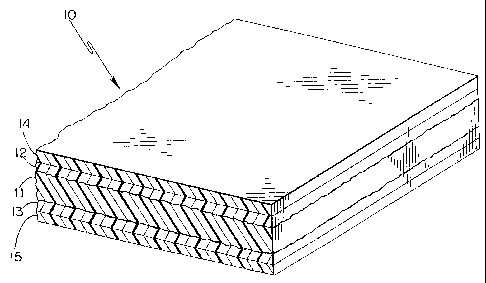
The drawing is a perspective view, partially irl
section, and on an enlarged scale illustrating a typical
interface mounting pad prepared in accordance with the
present invention, with the individual layers being shown
in section.
DESCRIPTION OF THE PREFERRED EMBODIMENT
In accordance with the preferred embodiment of the
present invention, and illustrated in the drawing, a
flexible plastic thermally conductive multi-layer
interface pad generally designated 10 is illustrated.
Pad 10 comprises a center or bulk layer 11 flanked by a
pair of thermally conductive surface skin layers 12 and
13 integrally bonded to opposed major surfaces of central
bulk layer 11. Additionally, release liners 14 and 15
are disposed on the outer surfaces of skin layers 12 and
13, thereby providing a protective layer for the surfaces
of the skin layers.
The bulk layer preferably comprises a blend of
siloxane polymers, including vinyl and hydride terminated
polymethylsiloxanes heavily filled with a finely divided
thermally conductive particulate. For most applications,
and assuming alumina as the particulate with a density of
3.75, the particulate present in the siloxane resin in a
range from between about 500 Phr to 2300 Phr. On a
volumetric scale, the particulate is present in an amount
ranging from between about 10 to 85% filler by volume,
with a range of between 20=~ and 80=~ being preferred. In
certain applications, the particulate may be selected as
a blend of particulate made up of two separate size
ranges. In one such application, the larger particulate
CA 02437243 2003-08-14
-6-
has an a~.~erage diameter of about 50 microns, which is
b--ended with smaller particulate having an average
diameter of approximately 2 microns. For most
applications, a somewhat larger particulate is utilized
in the bulk layer, generally greater than 2 microns. Tn
t'icse applications where it is utilized, the blend of
partiC-1.:C-ate assists in enha:-.cing the thermal properties
o'L'7 the bulk layer, with bi and tri models also being
usefl..I .
The skin layers have different physical and/or
chemical properties than the bulk compatible with the
bulk layer. Because of its higher cohesive strength, the
skin improves the physical properties of the overall pad.
T~:e blend of materials for the surface skin layers
includes thermally conductive particulate filler in a
lesser quantity than in the bulk, preferably in a range
of between about 5% and 60% by volume, with a range of
between 10% and 40% being preferred.
Tn overall preparation, it has been found preferable
to utilize a calendering operation to mate the skin
layers with the bulk layer. Other laminating operations
may be employed, if desired. For ease of material
handling, it is, of course, preferable that a release
liner be applied to the outer surfaces of the skin layers
in order to expedite the laminating or mating operation.
EXAMPLES
n order to facilitate an explanation of the
operation undertaken to prepare the multi-layer interface
pads of the present invention, the following specific
examples are provided.
CA 02437243 2003-08-14
-7-
(A) BULK LAYER
EXAMPLE I
Material Parts by Weight, Grams
Silicone elastomer with
modulus of 5-30 kPa (1-5 psi) 100
Alumina powder fillers 1200.
In actuai preparation, the reactant mixture is prepared
by thoroughly blending the resin components and fillers.
Thereafter, the reaction inhibitor and catalyst are
added. Thereafter, the reactant product is rolled or
otherwise leveled to a pad having a thickness of the
desired thickness, in this case, 10-250 mils. This pad
is highly filled, having low degree of cross-linking and
with a hardness of 30-60 Shore 00 and generally about 50
Shore 00. The mechanical properties render this pad
difficult to release off Teflon0 liners due primarily to
its low cohesive strength. The addition of the skin
layer facilitates the easy release of the composite from
a liner, and facilitates handling. A silicone release
liner with coated skin layer also helps in the production
of a pad using silicone gel resins in the above example.
In modified versions of the formulation of Example
I, the alumina powder filler may be increased to an
amount up to 2000 parts by weight (grams) depending upon
the thermal requirements and physical properties desired
in the bulk layer.
EXAMPLE II
Material Parts by Weight, Grams
Silicone elastomer with
modulus of 5-30 kPa (1-5 psi) 100
Alumina powder filler 224.
CA 02437243 2003-08-14
-8-
In actual preparation, the reactant mixture is prepared
by thoroughly blending the resin components and fillers.
Thereafter, the reaction inhibitor and catalyst are
added, after w~ich the reactant product is leveled or
rolled to a pad having a thickness of about 10-250 mils.
Th1s bulk material is lightlv cross-linked and soft with
a target hard::ess of 40 Shore 00. This product releases
well from Tefbut not from standard silicone release
liners.
EXAMPLE III
Material Parts by Weight, Grams
Silicone elastomer with
modulus of 5-30 kPa (1-5 psi) 100
Alumina pou.rder 242).
Alumina trihydrate powder 143.
In actual preparation, the reactant mixture is prepared
by thoroughly blending the resin components and fillers.
Thereafter, the reactioi: inhibitor and catalyst are
added, after w~i_ci; the reactant product is rolled to a
pad having a desired thickness of about 10-250 mils.
This is a low fill and elastic bulk materi al . Its
adhesion property which is greater than 50 g/in. on the
liner surface will result in stretching and severe
deformation of the material. This makes i_t impossible to
use after removal from the liners. The skin layers
reduce the entire composite release off standard liners
to less than 30 g/in.
CA 02437243 2003-08-14
-9-
EXAMPLE IV
Material Parts by Weight, Grams
Polybutadiene resin 100
Antioxidant 2
Catalyst 1.5
Alumina fillers 600.
This formula has a hardness of about 0 Shore 00. The
material adheres or sticks to commercially available
release liners and results in deformation of the pads at
thicknesses of 10-60 mils. The skin layer facilitates
easy rel-ease from standard silicone release liners at
less than 30 g/in. peel.
In certain formulations based upon this Example IV,
the quantity of alumina filler may be reduced to 200
parts by weight (grams) depending upo:: the required
thermal conductivity. Such formulations typically have a
hardness of about 40 Shore 00 and may be provided with a
skin layer to facilitate easy release from standard
silicone release liners.
(B) SKIN LAYER
EXAMPLE V
Material Parts by Weight, Grams
Microcrystalline wax 70
Ethylene-vinyl acetate
copolymer (EVA) 90
Aliphatic c-5 petroleum
hydrocarbon resin 100
Aromatic modi.fied c-5
hydrocarbon resin 100
Alumina 555.
The microcrystalline wax selected in this example has a
melting point of 55 C. and is commercially available
CA 02437243 2003-08-14
-10-
under the trade designation "M-7332" from Moore and
Munger Co. of Hartford, CT.
In certain variations of the formulation of this
Example V, the alumina content may range from between 100
par:~s by weight (grams) to an amount up to 720 parts by
weiuh~ (grams) depending upon the requisite thermal
performance and physical properties.
EXAMPLE VI
Material Parts by Weight, Grams
:Iicrocrystal line wax
(as in Example V) 70
Ethylene-vinyl acetate copolymer 90
Aliphatic c-:~ petroleum
hydrocarbon resin 100
Aromatic modified c-5
hydroca.rbon resin 100
Graphite 90.
T''ne formulation of Example V (skin) was ftzrther modified
bv lowering the quantity of thermally conductive
par--iculate filler employed was graphite in the quantity
ind~,cated. Results were comparable to that of Example V
(skin) but with slightly higher cohesive strength.
Ir1 variations of the formulation of this Example VI,
t;~:e graphite may be present in a range of between about
90 and 150 grams, but oreferably in a range of about 20%
by volume. The quantity of graphite is dependent upon
the thermal performance and physical properties desired.
CA 02437243 2003-08-14
-11-
EXAMPLE VII
Material Parts by Weight, Grams
Microcrvstalline wax
(melting poi;-it 55 C. ) 10
Silicone wax
(melting point 65 C.) 25
Alumina particulate 190.
This formulation enables better mating with the silicone
bulk layers and also provides hard protective layers.
EXAMPLE VIII
Material Parts by Weight, Grams
Silicone elastomer with
modulus of 30-70 kPa (5-10 psi) 100
Alumina powder fillers 150.
The formulation of Example VIII is utilized to prepare
skin layers for use with selected bulk layers, it being
noted that the elastomer selected for the bulk la;-er will
always have a modulus significantly less than that of the
skin layer. In this connection, the silicone elastomer
selected for the skin layer will typically have a modulus
of between about 20 - 70 kPa (5-10 psi) greater than that
of its mated bulk layer.
EXAMPLE IX
Material Parts by Weight, Grams
Silicone elastomer with
mociulus of 70-100 kPa (10-15 psi) 100
Alumina powder fillers 150.
The formu.lati_on of Example IX was similar to that of
Example VIII with the exception of the silicone elastomer
CA 02437243 2003-08-14
-12-
selected. In the formulation of Example IX, the selected
silicone elastomer had a modulus of 100-140 kPa (15-20
psi). The results achieved with the skin material
prepared from this formulation exhibited an increased
hardness over that obtained from the formulation of
Example VIII.
Each of the skin layer reactant products of Examples
I throagh IX inclusive may be applied to a release film
at a desired th'I~ckness, and thereafter placed in face-to-
face contact with the bulk layer to form upper and lower
sk4 ns of a pre-form. Similar or selected different skins
may be utilized for a given bulk layer, with the skin
selection depending, of course, upon the requirements of
the ultimate application, including mechanical properties
such as hardness, thermal properties, and the like. With
the release films in place on the outer surfaces, the
pre-form is then calendered to a desired finished
thickness, with handling being facilitated by the
presence of the release liners. Release liners employed
with the skin layers of the present invention are
preferably fabricated from standard silicone films or a
polyester film such as stress-oriented polyethylene
terephthalate (Teflon0).
BONDING TECHNIQUE
A skin layer comprising the reactant product of
Example IV was applied to the opposed major surfaces of
the bulk layer of Example I, with each exposed skin layer
being covered with a release liner of 1-5 mil silicone
release liner. A 3-mil silicone release liner has been
found well adapted for use with skin layers of between
0.3 mils and 3 mils. This composite was then passed
through a pair of coordinated pinch rolls and compressed
CA 02437243 2007-01-30
-13-
to an overall thickness of 5-20. The resultant was a
highly uniform flexible mounting pad having an overall or
composite thermal conductivity of 0.5-25 W/m-K. In one
application, a bulk layer having a thickness of 38 mils
(Example I) was flanked by skin layers of 1.0 each
(Example IV) each with release liners of 3.0 mil silicone
was passed through a pair of coordinated pinch rolls and
compressed to an overall thickness of 40 mils. It will
be appreciated that the ultimate thickness of the
composite laminate is determined by the specific
application contemplated for the product.
The mechanical properties of the pads were
excellent, with the release liner being readily removable
from the skin surface layers without any evidence of
blocking.
For most applications, the bulk layer will
preferably have a thickness of between about 5 and 250
mils, with a compatible skin being applied thereto. For
most purposes, a skin thickness ranging from-between
about 0.1 and 2 mils has been found useful. It will be
appreciated that the actual thickness selected for the
laminates having the thinner bulk material will
accordingly have the thinner skins applied thereto. The
conve-rse is true for those components with greater
thickness dimensions.
It will be appreciated, therefore, that the above
examples are presented for illustration purposes only and
are not to be construed as a limitation upon the scope of
the claims to which this invention may be otherwise
entitled.