Note : Les descriptions sont présentées dans la langue officielle dans laquelle elles ont été soumises.
CA 02443790 2003-10-10
WO 02/088973 PCT/IB02/01168
-1-
Communication interface for an electronic device
Field of the Invention
The present invention relates to a communication interface for permitting an
electronic device to be in communication with another electronic device using
first
or second data transmission modes.
Background Art
A Universal Serial Bus (USB) standard has been developed which allows up to
127
peripheral devices such as printers, scanners, keyboards, modems, cameras and
storage devices to be attached to a host, usually a personal computer (PC),
through
a 4-wire bus. These devices can be connected to the PC either directly or via
hubs
which provide additional connections. USB has the advantage that connection of
different types of devices becomes standardised. Furthermore, a device can be
connected while the PC is switched on and while other devices are in use. USB
can
support data rates as high as 480 Mbps. An overview of USB may be found in
"USB Hardware & Software" by J. Garney et al. (Anna Books, 1998) [ISBN 0-
929392-3-X] and a current version of the USB specification is available at
www.usb.org or from USB-IF Administration, 5440 SW Westgate Drive, Suite 217,
Portland, OR 97221 USA.
Mobile telephone handsets are being introduced which support USB. A USB
interface allows them to be connected to a PC or a peripheral device. In this
way, a
handset may serve as a peripheral device or a host. Although such a handset
will
enjoy many of the advantages of USB, there are, however, some drawbacks.
Simple
peripheral devices for connecting to the handset are made unnecessarily
complex
and expensive since they themselves must support USB. Furthermore, once
connected, these devices draw a high current from the handset, which has
limited
power resources.
Mobile telephone handsets are known which have simple serial communications
interfaces based on the RS-232 standard and which use single-ended data
transmission. This allows them to be connected to peripheral devices such as
CA 02443790 2010-10-06
-2-
keyboards for entering text for short message service (SMS) and e-mail. These
types of
interfaces draw much less current and so are better suited to low power
applications.
To overcome the drawbacks of having a USB interface, both types of interface
may be
included in a single handset. However, this is not practical for a small
handset.
Furthermore, this defeats the object of providing a standardised connector.
The present invention seeks to provide a solution to this problem.
Disclosure of the Invention
According to the present invention there is provided a universal serial bus
(USB)
communication interface configured to provide for communication between an
electronic
device with another electronic device using first or second data transmission
modes,
wherein said first data transmission mode comprises single-ended asynchronous
data
transmission and wherein said second data transmission mode comprises USB
differential
transmission of data, the interface comprising:
first communication circuitry for communication using said first data
transmission
mode;
second communication circuitry for communication using said second data
trasmission mode;
switching circuitry configured to selectively connect the first/second
communication
circuitry to a common transmission path based on determining circuitry for
determining the
mode of data transmission on said common transmission path; and
a USB port configured to physically conform to a USB specification for
receiving a
data bus, the USB port including power and ground lines and first and second
data lines, the
first and second data lines forming part of the common transmission path,
wherein the interface is configured to:
use the first and second data lines for data transmission in said second USB
differential data transmission mode and in said first single-ended
asynchronous data
transmission mode without the need for an interface adapter, the first single
ended
asynchronous data transmission mode providing for use of one of said first and
second data
lines only to receive data and the other of said first and second data lines
only to transmit
data, and the second USB differential transmission mode providing for use of
each of said
first and second data lines both to transmit and receive data;
i
CA 02443790 2010-10-06
-3-
use a first set of voltage levels along the data lines in said first mode of
data
transmission mode; and
use a second different set of voltage levels along the data lines in said
second
data transmission mode, and
wherein said switching circuitry is configured to shift the first or second
set of
voltage levels of the data lines between the two sets of voltage levels.
The first and second data lines may be used to transmit and receive data using
the second
mode of data transmission. The first data line may be used to receive data and
the second
data line may be used to transmit data using the first mode of data
transmission. The first
data line may be used to receive and transmit data using the first mode of
data transmission.
The second data line may be used to receive and transmit data using the first
mode of data
transmission. The first and second data lines may comprise D+ and D-lines
respectively.
The first and second data lines may be connectable to a data bus.
The first mode of data transmission may use a first set of voltage levels,
while the second
mode of data transmission may use a second, different set of voltage levels.
The switching means may comprise means for shifting the first or second set of
voltage
levels to another set of voltage level.
The interface may further comprise means for determining the mode of data
transmission
on said common transmission path.
The means for determining the mode of data transmission may comprise means for
sensing
a status line. The means for determining the mode of data transmission may
comprise
means for detecting a power supply line.
The first communication means may be configured for full-or half-duplex
communication.
The interface may be incorporated into the electronic device.
According to the present invention there is also provided an electronic device
including an
interface. The electronic device may be portable and may be a mobile telephone
handset, a
i
CA 02443790 2010-10-06
-3a-
personal digital assistant or a mobile communicator, a digital camera, an MP3
player or a
handheld gaming system.
According to the present invention there is provided a USB communication
interface
configured to provide for communication between an electronic device with
another
electronic device using first or second data transmission modes, wherein said
first data
transmission mode comprises single-ended asynchronous data transmission and
said second
data transmission mode comprises USB differential transmission of data, the
interface
comprising:
means for communicating using said first data transmission mode;
means for communicating using said second data transmission mode;
means for selectively connecting the first/second communication means to a
common transmission path based on means for determining the mode of data
transmission
on said common transmission path; and
means for USB connection configured to physically conform to a USB
specification
for receiving a data bus, the means for USB connection including power and
ground lines
and first and second data lines, the first and second data lines forming part
of the common
transmission path;
wherein the means for a USB interface is configured to:
use the first and second data lines for data transmission in said second USB
differential data transmission mode and in said first single-ended
asynchronous data
transmission mode without the need for an interface adapter, the first single-
ended
asynchronous data transmission mode providing for the use of one of said first
and second
data lines only to receive data and the other of said first and second data
lines only to
transmit data, and the second USB differential transmission mode providing for
the use of
each of said first and second data lines both to transmit and receive data;
use a first set of voltage levels along the data lines in said first data
transmission mode; and
use a second, different set of voltage levels along the data lines in said
second data transmission mode, and
wherein said means for selectively connecting is configured to shift the first
or
second set of voltage levels of the data lines between the two sets of voltage
levels.
CA 02443790 2010-10-06
-3b-
According to the present invention there is also provided a method of
providing for
communication of an electronic device with another electronic device using a
USB
communication interface and using first or second data transmission modes,
said first data
transmission mode comprising single-ended asynchronous data transmission and
said
second data transmission mode comprising USB differential transmission of
data, the USB
communication interface comprising:
first communication circuitry to communicate using said first data
transmission
mode;
second communication circuitry to communicate using said second data
transmission mode;
switching circuitry to selectively connect the first/second communication
circuitry
to a common transmission path based on determining circuitry for determining
the mode of
data transmission on said common transmission path; and
a USB port configured to physically conform to a USB specification for
receiving a
data bus, the USB port including power and ground lines and first and second
data lines, the
first and second data lines forming part of the common transmission path;
the method comprising:
providing the first and second data lines to be used in data transmission in
said second USB differential data transmission mode and in said first single-
ended
asynchronous data transmission mode without the need for an interface adapter,
the first
single-ended asynchronous data transmission mode providing for the use of one
of said first
and second data lines to only to receive data and the other of said first and
second data lines
only to transmit data, the second USB differential transmission mode providing
for the use
of each of said first and second data lines both to transmit and receive data;
using a first set of voltage levels along the data lines in said first data
transmission mode;
using a second, different set of voltage levels along the data lines in said
second data transmission mode; and
using said switching circuitry to shift the first or second set of voltage
levels of the
data lines between the two sets of voltage levels.
CA 02443790 2003-10-10
WO 02/088973 PCT/IB02/01168
4-
Brief Description of the Drawings
An embodiment of the present invention will now be described, by way of
example,
with reference to the accompanying drawings in which:-
Figure 1 is a perspective view of a mobile telephone handset;
Figure 2 is a schematic diagram of mobile telephone circuitry;
Figure 3 is a schematic diagram of serial input/output circuitry;
Figure 4 is a schematic diagram of transceiver circuitry;
Figure 5 shows connection of a keyboard to a mobile telephone using single-
ended
data transmission and
Figure 6 shows connection of a personal computer to a mobile telephone handset
using bi-directional, differential data transmission.
Best Mode for Carrying Out the Invention
Referring to Figures 1 and 2, a mobile telephone handset 1 comprises a casing
2, a
battery pack 3, liquid crystal display (LCD) panel 4, a microphone 5, an
earpiece 6,
keypad 7, a connector 8, antenna 9, subscriber identification module (SIM)
card 10
and SIM card reader 11. Mobile telephone circuitry includes radio interface
circuitry 12, codec circuitry 13, controller 14, memory 15 and input/output
(I/O)
transceiver circuitry 16. The I/O transceiver circuitry 16 allows single-ended
(SE)
and USB modes of serial data transmission.
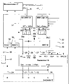
Referring to Figure 3, the I/O transceiver circuitry 16 includes a
microcontroller
unit (MCU) 17, a system application specific integrated circuit (ASIC) 18 and
a
transceiver circuit 19. In this example, the connector 8 is suitable for
connecting
the handset 1 to a USB host (not shown) and conforms to the USB specification.
It
will be appreciated that a so-called `B'-type plug may be used on the end of a
connecting cable to connect the handset 1 to a USB peripheral device. The
connector 8 is also suitable for connecting the handset 1 to other types of
peripheral device (not shown) which use SE modes of data transmission. A mode
of data transmission refers to an arrangement for transferring data between
two
entities, such as devices or circuits, and which may include hardware and
software.
CA 02443790 2003-10-10
WO 02/088973 PCT/IB02/01168
5-
The connector 8 is a USB port having power (Vbus) and ground (GND) lines 20,
21
and a pair of data lines 22, 23 referred to as D+/RxD and D-/TxD. The
connector
8 also has a status line (Id) 24 for determining the mode of data transmission
between the handset 1 and an attached device (not shown). The power, ground
and
data lines 20, 21, 22, 23 feed into the transceiver circuit 19.
The transceiver circuit 19 can operate in two transmission modes, namely USB
and
SE transmission modes. Each transmission mode has its advantages. USB
transmission uses a differential data transmission scheme which is used to
achieve
good noise rejection especially at high data rates. Meanwhile, SE
transmission,
unlike USB transmission, does not have strict timing requirements.
Furthermore,
SE transmission does not require a peripheral device, such as a keyboard
(Figure 5)
to have or be provided with a 5-volt power source.
The transceiver circuit 19 serves as an interface between the system ASIC 18
and a
data bus (not shown) connected to the connector 8. The transceiver circuit 19
level
shifts and conditions data and so allows the handset 1 to be used with
peripheral
devices having either type of interface. For example, level shifting may
include
converting signals between relatively low voltages used by the ASIC 18 and
relatively high voltages used for USB transmission, while signal conditioning
may
include setting rise and fall times on the D+/RxD and D-/TxD lines 22, 23.
The transceiver circuit 19 can be switched into USB transmission mode by
applying
a binary `0' signal to a SE mode line 25 and into SE transmission mode by
applying
a `1'. The transceiver circuit 19 supports first and second data paths
(FseO/FTX,
Vp/FRX) 26, 27 for receiving and transmitting data to and from the system ASIC
18. The relationship between the FseO/FTX and Vp/FRX data paths 26, 27 and the
D+/RxD and D-/TxD 22, 23 will be described in more detail later.
The transceiver circuit 19 is also provided with a plurality of USB-specific
data and
control lines. These include a received data line Vm 28 which provides a path
for
data received over the D-/TxD line 23, a differential received data line RCV
29, a
transmit/receive control line OE# 30 for controlling whether data is
transmitted or
CA 02443790 2003-10-10
WO 02/088973 PCT/IB02/01168
-6-
received, a transmit data line Vo 31 and a speed control line SPEED 32 which
selects a transmitted data slew rate. In this example, the transmitted data
slew rate
may be between 4 and 20ns or between 75 and 300ns.
The system ASIC 18 includes a single-ended universal asynchronous
receiver/transmitter circuit (SE UART) 33 and Universal Serial Bus (USB) logic
circuit 34. The USB logic circuit 34 encodes and decodes USB data commands.
The FseO/FTX and Vp/FRX data paths 26, 27 are switched between the SE UART
and the USB logic circuits 33, 34 by first and second pairs of switches 35a,
35b, 36a,
36b respectively controlled by a control line 37 from the MCU 17. The control
line
37 also provides the signal through the SE mode line 25. The system ASIC 18
also
includes a first detection circuit 38, which measures the resistance of the
status line
Id 24 on the connector 8 to determine the type of data transmission used by an
attached device (not shown). The status line Id 24 is connected to a handset
power
supply 39, for example battery 3, through a weak pull-up resistor 40. In this
example, the resistor 40 has a value of 220 M. It will be appreciated that
instead of
measuring resistance, a signalling scheme may also be used. The system ASIC 18
may include a second detection circuit 382 which is connected to Vbus power
line
23. The detection circuits 38 report to the MCU 17, which is thus able to
determine
the mode of data transmission.
The SE UART circuit 33 has SETx line 39 for transmitting data to the attached
device (not shown) and a SERx line 40 for receiving data from the attached
device
(not shown).
The USB logic circuit 34 has a Se0_o line 43 for applying a signalling state
SEO to
the FseO/FTX line 26 so as to cause D+/RxD and D-/TxD lines 22, 23 to be
driven at 0 volts and a Rxdp_i line 42 for detecting received D+ data.
The SE UART and USB logic circuits 33, 34 exchange command and transmission
data with the MCU 17 by means of first and second buses 44, 45.
CA 02443790 2003-10-10
WO 02/088973 PCT/IB02/01168
-7-
It will be appreciated that the transceiver circuit 19 may be modified, for
example it
may be provided with different data and control lines configurations. For
example,
the FseO/FTX data line 26 and the transmit data line Vo 31 may be replaced by
a
FseO line and a Vo/FTX line respectively. As a result, the FseO lines serves a
single
function, namely to apply the SEO signalling state in USB mode as described
above.
The Vo/FTX line has a dual function, namely to provide a transmit data line Vo
as
described above or a conventional TxD SE line as described below. This
configuration requires modification of the ASIC 18, especially the switches
35, 36.
Consequently, the Se0_o line 41 is permanently connected to the FseO line. The
Vo/FTX line is connected to SETx line 39 of the UART 33 through the switch 35a
and also to a TxD_o line (not shown) of the USB logic circuit 34 through a
switch
(not shown) which is controlled by the control line 37.
Referring to Figure 4, the transceiver circuit 19 exchanges signals with the
system
ASIC 19 at voltages Vio. The transceiver circuit 19 exchanges signals with an
attached device (not shown), when in USB mode, at a nominal voltage of 3.3V,
and,
when in SE mode, at a voltage of Vreg. In this example, Vio < 3.3V and Vio <
Vreg. Thus, the transceiver circuit 19 level shifts signals between the ASIC
19 and
the attached device (not shown).
The transceiver circuit 19 comprises first and second output means 46, 47. The
transmit/ receive control line OE# 30 enables the output means 46, 47 to
transmit
data, while the speed control line 32 determines the slew rate of the
transmitted
data.
In USB mode, the first output means 46 is supplied with transmission data from
the
USB transmit line Vo 31 from the USB logic circuit 34 and with a signal SEO
along
the first data path FseO/FTX 26. The second output means 47 is also supplied
with
transmission data from the USB transmit line Vo 31. The signal SEO is used to
control the first and second output means 46, 47 so as to drive D+ = D- = OV.
Thus, the D+/RxD and D-/TxD lines 22, 23 operate as D+ and D- respectively as
conventional USB data lines.
CA 02443790 2003-10-10
WO 02/088973 PCT/IB02/01168
8-
In SE mode, the first output means 46 is supplied with transmission data from
the
first data path FseO/FTX 26 from the SE UART 33. The signal SE mode 25 is used
to switch the first and second output means 46, 47 into SE mode. Thus, the D-
/TxD line 23 operates as TxD as a conventional SE line.
The transceiver 19 further comprises first, second and third input means 48,
49, 50.
In USB mode, the first input means 48 is supplied with received data from the
D-
/TxD line 23. It supplies the data to the USB logic 34 circuit using received
data
line Vm 28. Similarly, the second input means 49 is supplied with received
data
from the D+/RxD line 22. Again it passes the data to the USB logic circuit 34
using the second data line Vp/FRX 27. The third input means 50 receives data
from both D+/RxD line 22 and D-/TxD line 23 and supplies a differential
received data signal RCV to the USB logic circuit 34.
In SE mode, the second input means 49 is supplied with received data from the
D+/RxD line 22. It supplies the data to the SE UART circuit 33 using second
data
line Vp/FRX 27.
In addition to switching data, the input and output means 48, 49, 50, 46, 47
also
perform level shifting and signal conditioning on data received and
transmitted to
and from the attached device (not shown).
For shifting voltage levels of the received and transmitted signals, the
transceiver
circuit 19 is provided with voltage reference sources. While the handset is
powered,
the circuit 19 is continuously provided with a source Vio 51, while a source
Vref 52
is controlled by the MCU 17. Vbus 20 is provided through the connector 8.
Thus,
in SE mode, the transceiver circuit 19 is supplied with voltage sources Vio 51
and
Vreg 52, while in USB mode, it is provided with voltages sources Vio 51 and
Vbus
20.
SE and USB modes of transmission will now be described.
CA 02443790 2003-10-10
WO 02/088973 PCT/IB02/01168
-9-
Referring to Figures 3 and 5, a keyboard 53 which communicates according to RS-
232 standard is connected to the handset 1 using the connector 8. The keyboard
53
has a resistor (not shown) which connects the status line 24 to ground. This
is
measured by the first detection circuit 38, and so the MCU 17 determines that
the
keyboard 53 is a simple peripheral device operating according to the single-
ended
transmission mode. The controller 17 applies a `1' to the control line 37,
which
switches the transceiver 19 to SE transmission mode. The high signal on the
control line 37 switches the data paths 26, 27 to the SETx and SERx lines 39,
40
respectively of the SE UART 33. As a result the D+ line 22 of the connector 8
is
driven as a receive (Rx) line, while the D- line 23 of the connector 8 is
driven as a
transmit (Tx) line.
Referring to Figures 3 and 6, the handset 1 is connected using a USB cable 54
to a
port 55 of a USB hub 56. The hub 56 is connected to a personal computer (not
shown) by a cable 57. The status line 24 is unconnected and left to float at
Vio.
The second detection circuit 382 detects Vbus and so the microcontroller 17
determines that the handset 1 is connected to a USB host and should therefore
operate according to USB transmission mode. The controller 17 applies a `0' to
the
control line 37, which switches the transceiver 19 to USB transmission mode.
The
low signal on the control line 37 switches the data paths 26, 27 to the Se0_o
and
Rxdp_i lines 39, 40 respectively of the USB logic circuit 34. As a result the
D+ and
D- lines 22, 23 are used in conventional USB transmission mode. It will be
appreciated that the handset 1 can be connected directly to a personal
computer.
This has the advantage that a USB interface can be used and still have
backward
compatibility with systems which operate according to SE transmission. There
is no
need to provide additional pins or connectors.
In the example hereinbefore described, in SE mode, one line 22 is used for Rx
and
the other line 23 is employed for Tx. This allows the handset 1 to transmit
and
receive signals simultaneously with another device, i.e. full-duplex
communication.
However, one or both lines 22, 23 may be configured for half-duplex operation
with
one or more devices. For example, if each line 22, 23 is used for both
transmitting
CA 02443790 2003-10-10
WO 02/088973 PCT/IB02/01168
-10-
and receiving in SE mode, i.e. half-duplex communication, then they can be
used
independently of one another and so permit the handset 1 to communicate with
two
other devices. The lines 22, 23 may be used for half-duplex communication with
the same device. During half-duplex communication, the lines 22, 23 may
transmit
signals from the handset 1 at the same or different times.
It will be appreciated that many modifications may be made to the embodiment
hereinbefore described. Many types of portable digital equipment may be used
instead of a mobile telephone handset, such as a personal digital assistant, a
digital
camera, an MP3 player or a portable gaming system. The host need not be
personal
computer but may be, for example, a games console such as Sony Playstation 2
or
Microsoft X-box. The MCU and/or the transceiver circuit may be integrated into
the system ASIC. Different signals may be used to switch the transceiver
circuit
between USB and SE modes. For example, the transceiver circuit can be switched
into USB mode by application of a `1' to the SE mode line and into SE mode by
use
of a `0'. Alternatively, a more complicated signalling arrangement using data
bus
communication may be used.