Note : Les descriptions sont présentées dans la langue officielle dans laquelle elles ont été soumises.
CA 02451030 2003-12-19
WO 03/001260 PCT/US02/19562
OPTICAL SWITCHES AND ROUTERS AND OPTICAL FILTERS
This is a PCT Application which claims priority to U.S. Application No.
09/886,698,
filed June 20, 2001, U.S. Application No. 101118,532, filed April 8, 2002,
U.S. Application No.
10/118,531, filed April 8, 2002, U.S. Application No. 10/118,709, filed April
8, 2002, and U.S.
Application No. 101118,760, filed April 8, 2002, the entire contents of which
are herein
incorporated by reference.
BACKGROUND OF THE INVENTION
Throughout this application various publications are noted. The disclosures of
these
publications in their entireties are hereby incorporated by reference in this
application in order to
more fully describe the state of the art to which this invention pertains.
1. Field of the Invention
The present application discloses one or more inventions. The inventions
relate generally
to optical switching, and in particular, one invention relates to methods,
devices and systems to
optically switch a specific channel of light between optical fibers. Other
inventions generally
relate to the "on/off' switching of optical filters, which are specific for a
signal in one
wavelength or in one channel within a band of signals or band of channels,
respectively.
2. Description of the Related Art
Dielectric microspheres are known in the art. It has been shown that a
microsphere of the
appropriate proportions can form a wavelength specific connection from one
optical fiber to
another by virtue of the dielectric microsphere's resonance in a whispering
gallery mode (WGM)
for the specific wavelength, or for a group of specific wavelengths of light
which are the resonate
frequencies. The WGM may be used to switch light transmission from one optical
fiber to
another. Depending on the placement of the microsphere and nature of the
optical fibers, fairly
high coupling efficiency and light transfer may be achieved. This is disclosed
in "Highly
Efficient Optical Power Transfer to Whispering Gallery Modes by Use of a
Symmetrical Dual
Coupling Configuration", Ming, Cai and Kerry, Vahala, Opt. Lett 25, No. 4, 260
(2000).
-1-
CA 02451030 2003-12-19
WO 03/001260 PCT/US02/19562
Wavelength Division Multiplexing (WDM) is a technique which has been used to
enhance the signal capacity of a single mode optical fiber by simultaneously
transmitting
multiple discreet wavelengths of light, referred to as "channels" in a single
band. The
wavelengths in each channel are separated by a pre-determined spacing, usually
on the order of
hundreds of GHZ. Dense Wavelength Division Multiplexing (DWDM) systems are
characterized by closer spacing between the respective wavelengths comprising
the channels
thereby allowing for a greater number of channels within the same band in the
same optical fiber
as compared to WDM.
The speed of routing from one optical fiber to another is limited by the rate
at which the
optical switching occurs. In the past, switches which convert the optical data
to electronic data
have been a "bottleneck" in the system. Those acquainted with optical
switching will recall that
much interest has been shoran in achieving the goal of a direct optical to
optical switch which
would eliminate the bottleneck caused by the optical to electronic conversions
of the past. A
variety of devices have been developed in pursuit of achiemng-~nis goal.
Common to many optical to optical switches and optical routers is an all or
nothing
functionality by which the entire signal, within a channel, is switched or not
switched. While
useful for small or local networks, especially those networlcs with easily
controlled light sources
(lasers), in larger or less controlled environments, an optical muter must be
able to accept signals
from a variety of sources and seamlessly multiplex despite difference in the
quality of the
signals. Optical switches lacking the ability to monitor, equalize and/or
groom the channels in
nanoseconds or even picoseconds (which is "real time" for optical
transmissions). This may
yield turbidity within a band resulting in unbalanced light transmissions
(signals) from channel
to channel which in turn may cause noise, loss of part of a signal or channels
to drop out.
Accordingly, applicants have identified a need for an optical switch and muter
that
operate in "real time" (which is in the order of nanoseconds or picoseconds)
for light
transmission. Applicants have also identified a need for an optical router of
"real time" optical
switches which can monitor, groom, and/or balance a channel relative to the
other channels in an
optical band.
Further, with respect to the general field of dielectrics, it has been
described by Grie~ &
DufYesne in U.S. Patent 6,055,106 that small dielectric particles may be
contained in one or
more optical traps. As stated above, optical trapping is known and can be used
to contain and
manipulate small particles in the submicron to hundreds of micron range.
-2-
CA 02451030 2003-12-19
WO 03/001260 PCT/US02/19562
Depending on the placement of a WGM microsphere, the nature of the optical
fibers, and
the diameter or taper of the optical fibers, high efficiency of light transfer
may be achieved for
the resonate frequencies. See, "Highly efficient optical power tfAansfe~ to
whispe~ihg-gallery
modes by use of a symnaetrical dual coupling co~fzgu~atioh ", Mi~zg Cai and
Ke~sy Tlahala Opt.
LETT 25, No. 4, 260 (2000); "Phase-matched excitation of whispering-galley-
mode ~esonances
by a fibet~ taper ", J. C. Knight, G. Cheung, F. .Iacques, and T. A. Berks,
Opt. LETT 22, No. 15,
1129 (1997). Particular attention should be paid to Figure 2, and "Time-domain
obse~°vatioh of
optical pulse propagation in whispering-gallef y modes of glass spheres ", R.
W. Shaw, W. B.
Whitten, M.D. Bar~zes, and J.M. Ramsey, Opt. LETT. 23, No. 16, 1341 (1990.
In determining Q for a silica microsphere, physical factors which reduce Q
below the
limit defined by material losses Q-1 n,at are the losses attributable to Q-
l~o"t, Q lraa and Q-ls.s.
Wherein Q-l~ont are those losses due to surface contaminants, Q-lraa are those
losses attributable to
the smallness of the diameter of the microsphere and Q SS represents losses
due to scattering
caused by surface imperfections. Measurements of losses indicate that if the
diameter of a
microsphere divided by the wavelength of light it was resonating for is >_ 15
then Q-lraa is > 1011.
Additionally, for microspheres larger than 100 microns in diameter Q-ls.s is «
1 x 10⁻¹⁰.
"Ultimate Q of optical microsphe~e resonatof°s ", M.L. Gorodetsky, A.A.
SavclZenkov, and V.S.
Ilchenko Opt. LETT. 21, Na. 7, 453-455.
It has been described by Knight that a microsphere coupled to an optical fiber
with a
stripped off polymer coating (cladding) over a region of the optical fiber,
which has been drawn
out in a tapered waist region, can achieve high coupling efficiency in the
waist region. Coupling
is to the evanescent tail of a signal, extending out into the free space along
the region of the
optical fiber surrounding the taper. Knight reported a coupling efficiency of
a microsphere
resonator at a tapered waist region with measurements of Q as high as 5 * 10~.
One method to taper an optical fiber is to apply heat to an optical fiber and
cladding
above their respective melting temperatures so that it will stretch, and apply
a stretching force.
U.S. Patent 5,729,643 issued to Hmelar.
With respect to WDM, as stated above, the wavelengths in each channel are
separated by
a pre-determined spacing usually in the order of hundreds of GHz and with
transmission rates up
to about 10 Gb/s. DWDM systems are characterized by closer spacing in the
order of 50 to 12.5
GHz between the respective chamlels. The closer spacing allows for a greater
number of
chamnels within the same band in the same waveguide as compared to WDM, for
example 320
-3-
CA 02451030 2003-12-19
WO 03/001260 PCT/US02/19562
DWDM channels at 10 Gb/s yields a 3200 Gb/s fiber capacity as compared to 80
channels at 10
Gb/s which yields an 800 Gb/s fiber capacity.
In addition to WDM and DWDM, optical networks may increase fiber capacity with
time
division multiplexing (TDM). TDM can achieve a 3200 Gb/s fiber capacity by
combining less
channels and faster transmission rates. For example, 80 channels at 40 Gb/s
yields the 3200Gb/s
fiber capacity and maintains greater channel spacing by reducing the Bit
periods. However,
reduction of the Bit period from 10 Gb/s to 40 Gb/s reduces the window through
which to
measure waveform from 100 picoseconds to leave only a 25 picosecond window.
Plaotohics
Specty°a Septembe~° 2001, "Faster vs. Dehse~: Networks Reach
Ahothe~ Crossroads ", by Daniel
C. McCa~tlay. Therefore, in WDM, DWDM or TDM optical networks picoseconds
switching is
"optical real time".
Accordingly, there exists a need for an optical filter which has the ability
to select and
switch at least one specific wavelength light signal from among a group of
wavelength light
signals within an optical transmission band in "optical real time"; and which
can filter out in
"optical real time" specific wavelength light signals, from among all the
different wavelength
light signals which may be found within the channels of an optical
transmission band.
SUMMARY OF THE INVENTION
This application discloses one or more inventions.
One invention provides novel and improved methods, systems and devices to
rapidly (in
the range of nanoseconds and event picoseconds) switch a signal between
optical fibers by
coupling a dielectric microsphere, via whispering gallery mode resonance (WGM)
between
optical fibers. A selected signal from a particular channel within an optical
band can be
selectively switched by controlling a plurality of the optical switches. All
references made
hereinafter to microsphere(s) shall refer to dielectric microsphere(s).
hl all the embodiments of this invention which are shown, the optical muter is
formed of
a series of the optical switches. Common to the optical switches is a
microsphere in proximity to
the unclad or thinly clad regions of a pair of optical fibers. To switch the
signal of a particular
channel (wavelength of light) between optical fibers, the evanescent waves
emanating from the
-4-
CA 02451030 2003-12-19
WO 03/001260 PCT/US02/19562
electromagnetic fields associated with the signal traveling in an optical
band. A particular
channel couples with, and resonates across, a wavelength specific microsphere
via the WGM of
the microsphere to switch the signal to another optical fiber.
In one embodiment of the optical router, each microsphere forming an optical
switch has
a steady state index of refraction "n" and will resonate in WGM for a specific
wavelength of
light (channel).
The switching is accomplished by controlling the steady state index of
refraction "n" of
the microsphere. A microsphere is positioned between optical fibers, with
substantially similar
indexes of refraction at a region of thinned or removed cladding, suitable
optical fibers include
those tapered optical fibers identified by Cai & Yahala. A pair of electrodes,
placed on either
side of each microsphere, can be used to apply a voltage across the
microsphere. When an
adequate voltage is applied across the electrode pair the steady state index
of refraction "n" of
the microsphere is altered by the polarizing effect of the voltage on the
substrate of the
microsphere. The polarization changes the dielectric constant of the substrate
which in turn
alters the steady state index of refraction "n" of the microsphere. In the
case where the steady
state index of refraction "n" of the microsphere is substantially similar to
the index of refraction
of the optical fibers the voltage will cause the steady state index of
refraction "n" of the
microsphere to become sufficiently dissimilar from the index of refraction of
the optical fibers
thereby tending to preclude WGM resonance.
To switch a particular optical switch within the optical muter the voltage
across a
selected electrode pair need only be briefly interrupted ( in the order of a
few nanoseconds to a
few picoseconds) to allow the signal to resonate across the microsphere and
pass from one
optical fiber to another. Accordingly, an optical muter useful for WDM, DWDM
and
wavelength division de-multiplexing is achieved.
Conversely, by selecting a microsphere with a steady state index of refraction
"n"
dissimilar to the index of refraction of the optical fibers and applying
sufficient voltage across
the selected electrode pair to alter the steady state index of refraction "n"
of the microsphere to
be substantially similar to the index of refraction of the optical fibers WGM
resonance of the
microsphere is enabled via the application of the voltage.
Adjustment of the voltage may also provide for a controllable index of
refraction of "n ~
x," for the microsphere, wherein as "x" approaches zero the efficiency of the
transfer of signal
-5-
CA 02451030 2003-12-19
WO 03/001260 PCT/US02/19562
approaches the microsphere's maximum coupling efficiency which may be useful
for
applications such as channel equalizing, grooming and power balancing.
In another embodiment of the optical muter, a plurality of wavelength specific
microspheres are provided, each with a light activated material, such as a
dye, integrated within
their substrate. To form the optical muter, a series of optical switches, each
one containing a
known microsphere selected to resonate in WGM for a specific channel, are
positioned in close
proximity to an unclad or thinly clad region in each of two optical fibers.
Each optical switch operates by controlled irradiation of the microsphere with
an
appropriately intense beam of light. The irradiation activates the light
activated material and
depending on the selection of the light activated material and microsphere
substrate, the
irradiation will either change the dielectric constant of the light activated
material and affect the
average dielectric constant of the microsphere, or affect the dielectric
constant of the light
activated material and the substrate, thereby altering the dielectric constant
of the microsphere.
In either case, the change in the dielectric constant will alter the steady
state index of refraction
"n" of the microsphere.
If the steady state index of refraction "n" of the microsphere is
substantially similar to the
index of refraction of the optical fibers, the irradiation can be used to
alter the steady state index
of refraction "n" to become dissimilar to that of the optical fibers and
disrupt the WGM
resonance. A practical application of such a microsphere would be to maintain
an appropriately
intense beam of light directed at the microsphere until switching of the
channel corresponding to
that microsphere is required. A brief interruption in the intense beam of
light will result in
switching. On the other hand, if the steady state index of refraction "n" of
the microsphere is
dissimilar to the index of refraction of the optical fibers, a brief pulse of
irradiation can be used
to alter the index of refraction "n" of the microsphere to become
substantially similar to the
index of refraction of the optical fibers and thereby switch the channel by
enabling the WGM
resonance.
In either case, by pulsing the intense beam of light, "on" or "off ' in the
range of
nanoseconds to picoseconds, switching can occur in nanoseconds or picoseconds.
One pulse
mechanism which operates in the nanosecond and picosecond range is passing the
intense beam
of light through a Mach-Zender interferometer.
Moreover, adjustment of the intensity of the intense beam of light, in either
case, may
also provide for a controllable index of refraction of "n ~ x," for the
microsphere, wherein as "x"
-6-
CA 02451030 2003-12-19
WO 03/001260 PCT/US02/19562
approaches zero, the efficiency of the transfer of signal approaches the
microsphere's maximum
obtainable coupling efficiency which may be useful for applications such as
channel equalizing,
grooming and power balancing.
In another embodiment of an optical router, each microsphere comprising a
specific
optical switch has a steady state index of refraction "n" which always
corresponds to the index of
refraction of the optical fibers. Optical switching occurs when the selected
microsphere is
physically contained within an optical trap and moved towards the unclad or
thinly clad regions
of two optical fibers. At some proximity from the optical fibers the
evanescent wave associated
with the signal of the selected channel will resonate across the surface of
the selected
microsphere and switch signal one optical fiber to another optical fiber. When
the switching is
completed, the optical trap is withdrawn and the microsphere ceases to couple
to the fibers.
Adjustment of the proximity of the microsphere to the stripped or thinly clad
region of
the optical fibers may provide a controllable index of refraction of "n ~ x"
for the microsphere,
wherein as "x" approaches zero, the efficiency of the transfer of signal
approaches the
microsphere's maximum obtainable coupling efficiency which may be useful for
applications
such as channel equalizing, grooming and power balancing.
In each embodiment the switching and/or routing of the selected wavelength of
light
signal from one optical fiber to another is dependent on the propagation of an
evanescent wave
corresponding to a microsphere which acts in a WGM for the selected wavelength
of signal. The
switching "on" or "off' of the microsphere is either by physical movement or
by altering the
microsphere's steady state index of refraction "n".
Y'et other inventions disclosed in this application relate to methods,
apparatuses, and
systems, to filter at least one specific wavelength light signal from among a
group of light signals
within the different channels of an optical transmission band in "optical real
time".
In. one of the inventions, the optical filter uses a WGM resonate structure to
filter out a
specific wavelength light signal or a group of specific wavelength light
signals, and a WGM
control, or signal loss central to switch "on/off' the optical filter. If a
WGM control is used to
switch the optical filter "onloff', it is performed by blending the WGM
resonate structure into
the medium surrounding it without optical/electrical conversion. Further, a
single small WGM
resonate structure is used to resonate in WGM for which the only resonate
signal "RS" is within
the optical transmission band being filtered.
CA 02451030 2003-12-19
WO 03/001260 PCT/US02/19562
In another of the inventions, the optical filter is formed by placing a WGM
resonate
structure proximate to both an input waveguide from which it can receive input
light signal
transmissions and an output waveguide to receive the filtered light signal
transmission. The
optical filter is switched "onloff' by controlled signal absorbtion within a
WGM resonate
structure.
In yet another of the inventions, the optical filter is formed by connecting
two or more
subfilters, each containing a resonate structure. The optical filter is placed
proximate to an input
waveguide from which it can receive input light signal transmissions. The
filter can provide an
output consisting of a specific wavelength light signal transmission to an
output waveguide. The
optical filter of this invention may be always "on" or switched "on/off'.
Specifically, the first subfilter structure is the "gate keeper" and the
second is the
"isolator". Both the isolator and the gate keeper contain resonate structures
which can resonate
in WGM for a specific group of wavelengths of light known as resonate signals
"RS" (See the
table shown in FIG. 27). The filter results from having but a single RS,
within an optical
transmission band, common to the gate keeper and the isolator.
All references made herein to resonant structures shall be understood to
include those
structures constructed of a dielectric material including all materials with a
non-zero dielectric
constant which are not conductors. Preferably the selected dielectric material
is non-magnetic.
In some instances, depending on the paramters of the system, one of the two or
more resonate
structures may be a resonate cavity. For simplicity, and not as a limitation,
microspheres are
described and shown as the resonate structure in the detailed descriptions.
However, it should be
understood that any suitable resonate structure is anticipated and
combinations of different and
varying structures constructed of any suitable material and in differing and
varying numbers than
those depicted are also anticipated.
All references made hereinafter to waveguides shall be understood to be any
structure
adapted for transmitting an optical signal in a longitudinal direction which
provided for limited
loss of the optical signal during transmission. Waveguides shall be understood
to be any
structure adapted for the propagation of light signals in a longitudinal
direction. A waveguide, as
used herein, is a structure which provides an evanescent wave, corresponding
to the propagating
light waves .
_g_
CA 02451030 2003-12-19
WO 03/001260 PCT/US02/19562
A specific size resonate structure will resonate in WGM for a specific group
of RS which
corresponds to its effective size "de". Effective size is a function of actual
distance the light must
travel to complete a round trip within the resonate structure, represented as
"d", multiplied by the
index of refraction of the resonate structure "nrs". This relationship of d to
de is described in the
first equation:
Equation 1:
de - rirs * d
For a dielectric microsphere resonate structure, the wavelengths of each RS
which a
resonate structure (such as a gate keeper or isolator) constructed of a
specific size dielectric
microsphere will resonate for in WGM can be found by dividing the effective
distance the light
will travel in the microsphere by a non-zero integer "q" as shown in the
second equation:
Equation 2:
de/RS =q
and de/q =RS
Accordingly, the group of wavelengths of light (~,o, y, ~,2, . . . ~,") which
are the RS can
be calculated. Further, as the fixed diameter of a resonate structure is
reduced the number of RS
are reduced (see table in FIG. 27). The cost of this reduction in RS is to
increase the signal
losses due to Q-1 rad. However, by surrounding the resonate structure with the
appropriate
medium signal losses due to Q-1 rad may be reduced. The appropriate medium
should be one
which has an index of refraction "n",edium" which is adequately distinct from
nrs to establish the
condition of total internal reflection at the interface between the resonate
structure and the
medium.
-9-
CA 02451030 2003-12-19
WO 03/001260 PCT/US02/19562
Therefore, after identifying the signals within an optical telecommunications
band (in an
input waveguide) for which optical switching may be required (to an output
waveguide), the
appropriate WGM resonate structures to switch the identified signals can be
selected to construct
an optical filter. A group of "n" such optical filters may be combined to
multiplex (MUX) or
demultiplex (DEMUR) different wavelength optical signals, within different
channels of an
optical transmission band from a single waveguide to one or more other
waveguides or vice
versa, thereby optically cross connecting waveguides. Further, a group of "n"
such optical filters
may be combined to demultiplex a group of "n" signals from an input waveguide
to one or more
of "m" output waveguides. Additionally, a group of "n" filters can be used to
multiplex the
signals within "m" input waveguides into a single output waveguide.
In one of the inventions the optical filter may be always "on", or switched
"oWoff '.
"On/off' switching may be through one of two WGM controls or through a
controlled signal
loss. The controlled signal loss may be achieved by altering the imaginary
portion "is2" of the
dielectric constant of the resonate structure ors (see below).
In one of the inventions, the optical filter is switched "on/off" through a
WGM control.
The WGM control as illustrated is applied to several configurations in the
detailed description of
the preferred embodiments. The methodology of the WGM control is applicable to
dielectric
resonate structures in general. Accordingly, application of the WGM controls
to other dielectric
resonate structures, which support WGM resonance for signals within an optical
transmission or
optical telecommunication band, is within the intended scope of the
inventions.
In either the always "on" or the switched "on/off' case the selected resonate
structure
should have a minimum "Q" (quality factor) adequate to discern the separate
channels as spaced
in the optical transmission or telecommunication band supplying the signals to
be filtered.
Examples of connnonly referenced channel spacing structures found in a TDM,
WDM
and DWDM are as great as several hundred GHz or as narrow as 12.5 GHz. For 100
GHz
spacing the minimum Q needed to maintain channel separation is about 2000. For
50 GHz
spacing the minimum Q is about 4000 and for 12.5 GHz channel spacing the
minimum Q is
about 16,000.
-10-
CA 02451030 2003-12-19
WO 03/001260 PCT/US02/19562
"On/Off' Switching Control Through The WGM Control Cases
The first WGM control is used to switch "on/off' the filter through an
adjustment of nrs to
establish conditions which either support or do not support WGM resonance for
the desired RS.
Mechanisms for adjusting nrs include polarization of the resonant structure by
an applied
voltage or current causing a linear electro-optic effect or by an applied beam
of light causing an
optical effect. Those slcilled in the art will recall that a dielectric
structure has a dielectric
constant "s". The dielectric constant of a resonate structure "srs" can be
described as the sum of
a "real" portion "c1" and an imaginary portion "is2" as described in the third
equation.
Equation 3:
Ers = ~E1 '~ 1~2~
For those instances wherein is2 is small and remains unchanged, the index of
refraction of
the resonate structure nrs is known to be proportional to the square root of
the "real" portion of
the resonate structure dielectric constant ~El, Accordingly, nrs can be
altered through a
controlled change of s1 achieved by polarization. Further, from the first
equation it is l~nown that
when "d" remains fixed and nrs changes, de will change. Further, from the
second equation it is
known that the RS are a function of de/q and if de changes, a corresponding
change in RS the
resonate structure will resonate in WGM.
s1 can also be controlled by coating to the resonate structure with an
optically active
material such as molecules of liquid crystal, organic photorefractive
polymers, GaAs,
Nitrabenzene and LiNb03 which, upon application of a predetermined linear
electro optic effect
or optical effect, will alter the index of refraction of the coating material
which, for purposes of
effecting WGM resonance in a resonate structure, is the index of refraction of
that portion of the
resonate structure which is involved in the WGM resonance. A group of filters
can be combined
to multiplex or demultiplex a band of optical signals via optical cross
sections.
-11-
CA 02451030 2003-12-19
WO 03/001260 PCT/US02/19562
The second WGM control is used to switch "ouoff' the optical filter based on
an
adjustment of nrs of the resonate structure relative to the index of
refraction of a medium
"llmedium" surrounding at least one resonate structure waveguide interface, or
at least that portion
of the resonate structure at a region where coupling occurs, to establish
conditions which either
interrupt or encourage signal coupling or the coupling of light transmissions
between the
resonate structure or subfilters and the input and/or the output waveguide(s).
The mechanisms for adjusting the nrs is the same type of linear electro optic
effects and/or
optical effects used in the first WGM control. However, the adjustment in the
nrs is to effectively
blend the resonate structure into the medium.
The third WGM control is used to switch "on/off' the filter through an
adjustment of the
index of refraction of at least one of the resonate structures. The index of
refraction of the
resonate structure within the gate beeper subfiter, denoted "nrs~gate keeper)»
and the index of
refraction of the resonate structure within the isolator subfilter denoted
"nrs~'solator),~ establishes
conditions which either support or do not support WGM resonance for at least
the desired RS.
If, for example, the adjusted nrs corresponds to an nrs which supports WGM
resonance for
RS which are outside the telecommunications band or fox a group of RS with no
common signal
between the gate keeper and isolator, the signal will not switch through the
optical filter.
However, if the adjusted nrs supports WGM resonance for RS within the
telecommunications
band, one of which is also a RS of the gate beeper and isolator, the common RS
will switch
through the filter.
Mechanisms for adjusting llrs agate keeper) ~r nrs (isolator) include
polarization of the resonant
structure by an applied voltage or current causing a linear electro-optic
effect or by an applied
beam of light causing an optical effect.
The fourth WGM control is used to switch "on/off' the optical filter based on
an
ad ustment of n (gate keeper) pr n (isolator) relative to the index of
refraction of a medium "n "
rs rs medium
surrounding at least one resonate structure waveguide interface, to establish
conditions which
either interrupt or encourage signal coupling between the subfilters and the
input and/or the
output waveguide(s). The mechanisms for adjusting the nrs is the same type of
linear electro
optic effects and/or optical effects used in the first WGM control. However,
the adjustment in
the nrs is to effectively blend the resonate structure into the medium.
-12-
CA 02451030 2003-12-19
WO 03/001260 PCT/US02/19562
"On/Off' Switching Control Through Signal Loss
When a light signal is within a WGM resonate structure controlled signal loss
may be
achieved, as noted in Equation 3, by altering the imaginary portion "isz" of
the dielectric
constant of the resonate structure.
The mechanism of signal loss is to alter is2, through the absorption of signal
(light) by
triggering the action of light absorbing material within the substrate of
resonate structure. The
attenuation mechanism may tale place in concert with optical switching, or
separate therefrom.
By controlling only the imaginary portion "is2" of "srs", and because the
geometrical
configuration of the resonant structure is unchanged, the resonant structure
will continue to
support the same RS. However, internal to the resonant structure, an
absorption mechanism
converts the RS mode light to other forms of energy besides the specific mode
of the RS which it
previously supported.
"Onloff' switching of the filter through signal loss via the control of is2
does not require
a change in signal coupling the RS. Therefore, the dynamics of the coupling of
the resonate
structure to the light transmissions (signals) at the resonate structure-
waveguide interface need
not be altered.
The light absorbing material may be dihydroindolizines, diarylimylenes, ScGe,
bis-
Mienylperfluorocyclopentenes, spiropyrens, fulgides, quantum dots, doped semi-
conductor
nanoclusters, PL~LC, dyes, semi conductor nanoclusters, electrochromic
nanocrystals, semi
conductors, (nanocrystals have been shown to exhibit controlled IR
light/signal absorption in
response to an applied potential) "Elect~och~omic Nanoc~ystal Quafztum Dots ",
Congjuh Wang,
Moohsub Shim, Philippe Guyot-Sionn.est, SCIENCE hol. 291 page 2390 Mach 23,
2001) or
photochromic compounds such as photochromic bisthienylethene which can be
incorporated into
the substrate of the resonate structure and selectively activated by applying
the appropriate
quantity and/or quality of a trigger light or energy to cause absorption of
signal. "Optical
pf°openties avid dynamics of a photochoomic bisthief2yletl2e~ce in
solution ayzd i~c a polymer film ",
-13-
CA 02451030 2003-12-19
WO 03/001260 PCT/US02/19562
J. C. Owf~utsky, H.FI. Nelson, A.P. Baj°ohavski, O-K. Ki~a, G.M.
Tsivgoulis, S.L. Gilat ahd J.-M.
Lelara Che~aical Physical Letters 293 555-563. (1998).
The resonate structures described herein may be as small as a few microns. One
method
for positioung these small resonate structures is through the generation and
control of movable
of optical traps (as described by G~iey~ et al in U.S. Pateht 6, 055, ~ 06)
which can trap, contain,
position and hold small dielectric particles.
The above inventions may be employed in any application where the signal
transmitted
by the resonant structure is to be controlled thereby. For example, in an
assay format, the
resonant structure may be manufactured or modified post-manufacture by coating
with a binding
agent which binds to an analyte to be detected in a sample. In this invention,
the presence of the
analyte is detected by a change in frequency, attenuation or destruction of
the resulting signal
which comes about because of the binding of the analyte to the binding agent
on the resonant
structure upon exposure to the sample. Such a change in frequency ,
attenuation or destruction
of the resulting signal may also be accomplished in a biological assay by
competing away an
analyte bound to a binding agent on the resonant structure prior to exposure
to the sample.
Examples of binding agent/analyte pairs include antigen/antibody,
antibody/antigen,
ligand/receptor, receptorlligand, and nucleic acid/nucleic acid. Complexing
agents, chelating
agents and chemical bonding agents may also be employed.
Other features and advantages of the present invention will be set forth, in
part, in the
descriptions which follow and the accompanying drawings, wherein the preferred
embodiments
of the present invention are described and shown, and, in part, will become
apparent to those
skilled in the art upon examination of the following detailed description
taken in conjunction
with the accompanying drawings, or may be learned by practice of the present
invention. The
advantages of the present invention may be realized and attained by means of
the
instrumentalities and combinations particularly pointed out in the appendant
claims.
BRIEF DESCRIPTION OF THE DRAWINGS
FIG. 1 illustrates a component view of an optical router according to one
invention.
FIG. 2A illustrates an alternate embodiment of an optical muter.
- 14-
CA 02451030 2003-12-19
WO 03/001260 PCT/US02/19562
FIG. 2B illustrates a diagram of a component optical switch of the embodiment
of FIG.
2A.
FIG. 3A illustrates a partial perspective view of an alternate embodiment for
an optical
router.
FIG. 3B illustrates a cut away view along the line A-A of the embodiment of
FIG. 3A
showing an optical switch of the router in the "off' position.
FIG. 3C illustrates a cut away view along the line A-A of the embodiment of
FIG. 3A
showing an optical switch of the router in the "on" position.
FIG. 4 is a diagram of the optical muter and cornpoenents to generate optical
traps of
FIG. 3A.
FIG. 5 illustrates a component view of an optical switch and filter according
to another
invention.
FIG. 6 illustrates a component view of an electronically gated optical switch
and filter.
FIG. 7 illustrates a component view an optically gated optical switch and
filter.
FIG. 8 illustrates a component view of a signal loss optical switch and
filter.
FIG. 9 illustrates a component view of a DEMLTX system.
FIG. 10 illustrates an optical trapping system to manipulate optical switch
components.
FIG. 11A illustrates a component view of an optical filter according to
another invention.
FIG. I IB illustrates a component view of an optical filter according to
another invention.
FIG. 12 illustrates a component view of a demultiplexing system.
FIG. 13 illustrates an optical trapping system to manipulate optical switch
components.
FIG. 14 illustrates a component view of an optical filter according to another
invention.
FIG. 15 illustrates a component view of an electronically gated optical
filter.
FIG. 16 illustrates a component view an optically gated optical filter.
-ls-
CA 02451030 2003-12-19
WO 03/001260 PCT/US02/19562
FIG. 17 illustrates a component view of a signal loss switched optical filter.
FIG. 18 illustrates a component view of an optical filter with an intermediary
optical
fiber.
FIG. 19 illustrates a component view of a system of filters used to
demultiplex.
FIG. 20 illustrates a component view of an alternate embodiment of filters
used to
demultiplex.
FIG. 21 illustrates an optical trapping system to manipulate optical switch
components.
FIG. 22 illustrates a component view of an electronically gated filter
according to another
invention.
FIG. 23 illustrates a component view of an optically gated optical filter.
FIG. 24 illustrates a component view of a demultiplexing system.
FIG. 25 illustrates an optical trapping system to manipulate optical switch
components.
FIG. 26 is a table showing a relationship between microsphere diameter and WGM
resonate signals.
DETAILED DESCRIPTION OF THE PREFERRED EMBODIMENTS
Certain terminology will be used in the following specification for
convenience and
reference, and not as a limitation. Brief definitions are provided below:
A. An "evanescent wave" refers to a wave that occurs when a wave enters a
region in
which it cannot propagate. Typically such waves are characterized by an
amplitude which
decreases exponentially with distance into the region in which the wave cannot
propagate.
-16-
CA 02451030 2003-12-19
WO 03/001260 PCT/US02/19562
B. "WGM" refers to the whispering gallery mode, which is a property of
resonate
structures that can be used to form a wavelength specific optical conduit
between one or more
optical fibers and the resonate structure via evanescent waves.
C. "Beamlet" refers to a sub-beam of light or other source of energy that is
generated
by directing a light or other source of energy, such as that produced by a
laser or collimated
output from a light emitting diode, through a medium which diffracts it into
two or more sub-
beams. An example of a beamlet would be a lugher order laser beam diffracted
off of a grating.
D. "Phase profile" refers to the phase of light or other source of energy in a
cross-
section of a beam or a beamlet.
E. "Phase patterning" refers to a patterned phase shift imparted to a beam of
light, or a
beamlet which alters its phase profile, including, but not limited to, phase
modulation, mode
forming, splitting, diffracting, converging, diverging, shaping and otherwise
steering a beam or a
beamlet.
F. An "optical fiber" refers generally to an elongated structure of nominally
circular
cross section comprised of a "core" of relatively high refractive index
material surrounded by a
"cladding" of lower refractive index material, adapted for transmitting an
optical mode in the
longitudinal direction.
G. "WDM" refers generally to wavelength division multiplexing: a system
capable
of simultaneously transmitting data on several wavelength channels.
H. "DWDM" refers generally to dense wavelength division multiplexing: a system
capable of simultaneously transmitting data on several wavelength channels
with less spacing
between the channels than in a WDM system.
Although dielectric microspheres, which resonate in WGM for a group of
resonate
signals "RS", are described herein and shown in the figures, the illustrations
should not be
-17-
CA 02451030 2003-12-19
WO 03/001260 PCT/US02/19562
considered a limitation. Those skilled in the art will recognize that any
resonant structure which
supports a Q above the minimum Q required to maintain separation of the
channels in the optical
transmission band (the range of wavelengths in the "C" band are from about
1530 to 1565 nms ,
and in the "L" band are from about 1570 to 1620 nms) being filtered and/or
switched, which
may include structures such as stadiums, rings, hoops, oblate and prolate
spheroids, or discs
could be used in place of, or in conjunction with, dielectric microspheres.
In one invention regarding an optical roister, in the preferred embodiments,
an optical
roister is formed of a series of optical switches. Common to the optical
switches is the placement
of a microsphere in proximity to the unclad or thinly clad regions of a pair
of optical fibers to
achieve coupling of the microsphere to the optical fibers. To switch the
signal from a particular
channel (specific wavelength of light), between optical fibers, the WGM
resonmce of the
microsphere for evanescent waves emanating from the electromagnetic fields
associated with the
signal in the particular channel is controlled either by altering the
placement of the microsphere
or by altering the steady state index of refraction "n" of the microsphere.
To form the optical muter 10 illustrated in FIG. 1, a series of optical
switches 14, 16 and
18 are connected across a first and a second optical fiber F1 and F2. The
optical muter 10, by
virtue of the optical switches, is capable of optically routing a number of
different channels
within an optical band. Each channel contains a signal comprised of a distinct
wavelength of
light. Hence, the quantity of optical switches within the roister 10 will
define the number of
different channels that roister 10 can switch.
Each optical switch 12, 14 and 16 consists of a microsphere S 1, S2 or S3
positioned
between an electrode pair E & E' and placed in close proximity to a region of
thinned or stripped
cladding 20 on each optical fiber F1 & F2. Voltage is supplied to each
electrode pair E & E' via
-I8-
CA 02451030 2003-12-19
WO 03/001260 PCT/US02/19562
corresponding pairs of conductive leads 22, 24 and 26 which are attached to a
power supply (not
shown).
The channel specific functionality of each optical switch derives from the
selection of
appropriately sized microspheres. Appropriate size refers to the radius of the
microsphere
wherein ~ times the radius of the microsphere is approximately an integral %2
wavelength of the
wavelength of light the microsphere, with its steady state index of refraction
"n" resonates for in
WGM. Therefore, each microsphere by virtue of its size can be selected to
correspond to a
single channel carried within the optical band.
In the embodiment Shown lIl FIG. 1, the microspheres are selected with a
steady state
index of refraction "n" substantially similar to the index of refraction of
the optical fibers F1 &
F2. Or, stated in terms of optical switches, each microsphere is switched "on"
and will operate
in a WGM for an evanescent wave, emanating from an optical fiber, of a channel
with a signal
corresponding to the wavelength of light the given microsphere resonates for.
Therefore, absent
an adequate voltage across the electrodes pairs E & E', switching of the
signals from three
channels, corresponding to the wavelengths of light each microsphere S 1, S2
and S3 resonates
for, will occur via the WGM resonance of each of the three microspheres S 1,
S2 and S3 .
To achieve selected routing of signals within a channel adequate voltage
across each
electrode pair E & E' should be maintained until the switching of a specific
channel is desired.
The effect of applying adequate voltage across the electrode pairs E & E' is
to alter the steady
state index of refraction "n" of each microsphere S 1 - S3 by polarizing the
substrate forming the
microspheres. The polarization will change the dielectric constant of the
substrate which in tum
alters the steady state index of refraction "n" malting it sufficiently
dissimilar from the index of
refraction of the optical fibers to preclude WGM resonance and switching will
not occur.
-19--
CA 02451030 2003-12-19
WO 03/001260 PCT/US02/19562
When switching of a channel is desired, the voltage across a particular
electrode pair E &
E' surrounding the selected microsphere S 1, S2 or S3 is briefly terminated.
During that brief
termination the index of refraction "n" the microsphere return to its steady
state, which is
substantially similar to the index of refraction of the optical fibers F1 &
F2, thereby switching
and routing the appropriate channel.
Conversely, one may select microspheres which have a steady state index of
refraction
"n" substantially dissimilar to the index of refraction of the optical fibers
F1 & F2, whereby the
presence of adequate voltage across an electrode pair E & E' alters the index
of refraction "n' of
the select microsphere to become substantially similar to the index of
refraction of the optical
fibers F1 & F2, thereby switching and routing the appropriate channel. In
either case the
switching "on" or "off "of the voltage across the electrodes E & E' can be
accomplished in the
range of nanoseconds or even picoseconds, providing a system which can route a
channel in real
time. Any residual light transmission in a switched optical fiber may, as is
commonly the case,
be removed with an attenuator 28.
For a given channel, adjustment of the voltage may also provide for a
controllable index
of refraction of "n+x," for the microsphere, wherein as "x" approaches zero,
the efficiency of the
transfer of signal approaches the microsphere's maximum obtainable coupling
efficiency which
may be useful for applications such as channel equalizing, grooming and power
balancing.
In FIG. 1, for clarity, only three microspheres S1, S2 & S3 are shown and
three electrode
pairs 22, 24 & 26. However, it should be understood that a plurality of such
microspheres and
electrodes corresponding to the number of channels the muter 10 switches can
be provided. It
should also be understood, that one skilled in the art may combine both the
microspheres which
have a steady state index of refraction "n" substantially similar to the
optical fibers and those
-20-
CA 02451030 2003-12-19
WO 03/001260 PCT/US02/19562
microspheres that have a steady state index of refraction "n" which is
dissimilar to the optical
fibers into one router without departing from the intended scope of this
invention.
Illustrated in FIGS. 2A and 2B is another embodiment of the optical muter 30
and optical
switches 31. In this embodiment a plurality of microspheres S 1-S7 are placed
in close proximity
to a first optical fiber F1 and a second optical fiber F2. The cladding 32 of
the optical fibers F1
& F2 is thinned or removed at the region of close proximity 34. Within the
substrate of each
microsphere is a light activated material, such as a dye, which can alter the
steady state index of
refraction "n" of the microspheres when adequately irradiated by an intense
beam of light.
Each optical switch operates by the WGM resonance of a microsphere, which may
be
controlled by altering the index of refraction "n" of the microsphere, such
that the evanescent
waves emanating from the electromagnetic fields associated with a signal in a
particular channel
within one optical fiber resonates in WGM across the surface of the selected
microsphere to a
channel in another the optical fiber.
Depending on the selection of the light activated material and the material
comprising the
substrate of the microsphere, the irradiation will either change the
dielectric constant of the light
activated material and thereby effect the average dielectric constant of the
microsphere, or the
irradiation will effect the dielectric constant of the light activated
material and the substrate
thereby altering the dielectric constant of the microsphere. In both cases the
change in the
dielectric constant will alter the steady state index of refraction "n" of the
microsphere.
Generally, the size of each microsphere Sl-S7 corresponds to the wavelength of
light
(channel) the microsphere can effectively resonate for in WGM. Therefore, an
optical router 30
with seven distinctly sized microspheres forming seven optical switches 31 can
route up to seven
chamlels. The exemplary number of microspheres should not be viewed as a
limitation on the
number of microspheres which may be placed within a router of the invention.
Control of the
-21-
CA 02451030 2003-12-19
WO 03/001260 PCT/US02/19562
optical routing is accomplished by controlling the optical switches 31, which
in turn is
accomplished by altering the steady state index of refraction "n" of a
selected microsphere within
a selected optical switch 31, by either irradiation of the microsphere with an
intense beam of
light or by briefly terminating such irradiation.
In a "dissimilar" configuration the steady state index of refraction "n' of
the microspheres
S I-S7 is substantially dissimilar to the index of refraction of optical
fibers FI & F2. To optically
couple the given microsphere and thereby switch signal between optical fibers
F1 & F2, an
adequately intense beam of light directed at the appropriate microsphere in
the optical muter 30
will alter the steady state index of refraction "n' of the microsphere to
become substantially
similar to the index of refraction of the optical fibers F1 & F2 thereby
switching signal between
optical fibers via WGM resonance.
In a "similar" configuration the steady state index of refraction "n' of the
microsphere is
substantially similar to the index of refraction of optical fibers F1 & F2. To
optically couple a
given microsphere and thereby switch signal between optical fibers F1 & F2 the
adequately
intense beam of light directed at the selected microspheres within the muter
30 is terminated,
thereby allowing the index of refraction "n' of the microsphere to return to
its steady state which
is substantially similar to the index of refraction of the optical fibers F1 &
F2, and switching
signal between optical fibers via WGM resonance will occur.
The irradiation of the microspheres S 1-S7 within the optical switches 31 of
the optical
muter 30 may be accomplished with a laser beam 36a & 36b passing through an
illuminating
fiber 37. For each optical switch 31 (FIG. 2B) the laser beam 36a passes
through a Mach-
Zender interferometer 3S whereby the laser beam 36a is either intensified
through constructive
interference or weakened through destructive interference. Because the Mach-
Zender
interferometer 3~ operates in a matter of a few nanoseconds or even
picoseconds the adequately
CA 02451030 2003-12-19
WO 03/001260 PCT/US02/19562
intense beam of light directed at a selected microsphere can occur or be
terminated for a brief
period of time, thereby allowing for rapid optical switching and routing. A
computer 40 is used
to control the Mach-Zender interferometer 38 and to select which microsphere
to enable WGM
resonance in. Any residual light transmission in a switched optical fiber may,
as is cormnonly
the case, be removed with an attenuator 42.
Monitoring; equalizing, grooming and channel balancing Within a given chamlel
may be
accomplished by adjusting the intensity of the laser beams 36a or 36b
irradiating the
microspheres to control the index of refraction of "n ~ x," for the
microsphere, wherein as "x"
approaches zero, the efficiency of the transfer of the light within the
channel approaches the
microsphere's maximum obtainable coupling efficiency
Illustrated in FIG. 3A is an optical muter, generally designated 50, which
contains a
series of optical switches 51 each operating by the movement of microspheres
S1, S2 or S3 in
and out of close proximity with an unclad or thinly clad region 52 of a first
and second optical
fiber F1 & F2 (FIGS_ 3B and 3C). Each microsphere has a steady state index of
refraction "n"
substantially similar to the index of refraction of the unclad or thinly clad
region of the optical
fibers F1 & F2 that the optical muter 50 switches optical signals between.
Generally, the size of each microsphere S 1-S3 corresponds to the wavelength
of light
(channel) the microsphere can effectively resonate for in WGM. An optical
muter 50 with three
optical switches ~ 1, each with a microsphere of a different size, can route
up to three channels.
Only three microspheres are shown for clarity, however, it should be
understood by those skilled
in the art that a gr eater or lesser number of microspheres of preselected
sizes can be selected to
form the muter without departing from the scope of the invention. The movement
of the
microspheres S1, S2 or S3 is controlled by containing each microsphere S1, S2
or S3 within an
array of independently movable optical traps T1, T2 and T3.
- 23
CA 02451030 2003-12-19
WO 03/001260 PCT/US02/19562
Optical traps are produced by the gradient forces arising forrii passing
beamlets of light
through a high numerical aperture focusing lens 52 and converging each beamlet
of light. . The
formation of an array of independently movable optical traps .capable of
manipulating small
particles, such as microspheres is known in the art and therefore only an
overview description of
such formation is provided.
To route a signal from a channel in the first optical fiber F1 to a channel in
the second
optical fiber F2 the selected optical switch 51 is activated. To activate an
optical switch 51 the
selected microsphere S 1 initially held remote from the unclad or thinly clad
regions 53 of the
first and second optical fibers F1 & F2 (FIG. 3B) is moved, with an optical
trap, into close
proximity (FIG. 3C) to the unclad or thinly clad regions S2 of the first
optical fiber and second
optical fiber F1 & F2.
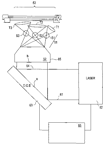
Shown in FIG. 4 is an overview of a system to generate and control the optical
traps used
to contain the dielectric microspheres S1-S3. The optical traps T1-T3 (FIG.
3A) are formed by
passing a collimated light, preferably a laser beam 61, produced by a laser 62
at area 'a' of a
beam altering optical element 63. The beam altering optical element diffracts
the laser beam 61
into a plurality of beamlets 64 each beamlet passing through area "b" at the
back aperture 65 of
the focusing lens 52 and containing a microsphere S 1-S3.
Any suitable laser can be used as the source of the laser beam 62. Useful
lasers include
solid state lasers, diode pumped laser, gas lasers, dye lasers, alexanderite
lasers, free electron
lasers, VCSEL lasers, diode lasers, Ti- Sapphire lasers, doped YAG lasers,
doped YLF lasers,
diode pumped YAG lasers and, flash lamp-pumped YAG lasers. Diode-pumped Nd:YAG
lasers
operating between 10 mW and 5 W are preferred.
When the laser beam 61 is directed at the beam altering optical element 63,
the beam
altering optical element produces the plurality of beamlets 64 by altering
phase profile of the
-24-
CA 02451030 2003-12-19
WO 03/001260 PCT/US02/19562
laser beam 61. Depending on the number and type of optical traps desired, the
alteration may
include diffraction, wavefront shaping, phase shifting, steering, diverging
and converging.
Suitable beam altering optical elements are characterized as transmissive or
reflective
depending on how they direct the focused beam of light or energy. Transmissive
diffractive
optical elements affect the beam of light or energy as it passes therethrough,
while reflective
diffractive optical elements affect the beam of light or energy as it is
reflected.
A beam altering optical element can also be categorized as being static or
dynamic.
Examples of suitable static beam altering optical elements include those with
one or more fixed
surface regions, such as gratings, holograms, stencils, Iight shaping
holographic filters,
polychromatic holograms, lenses, mirrors, prisms, waveplates and the like.
Examples of suitable dynamic beam altering optical elements having a time
dependent
aspect to their function include computer generated diffractive patterns,
phase shifting materials,
liquid crystal phase shifting arrays, micro-mirror arrays, piston mode micro-
mirror arrays, spatial
light modulators, electro-optic deflectors, accousto-optic modulators,
deformable mirrors,
reflective MEMS arrays and the like. With a dynamic beam altering optical
element, the media
which comprises the beam altering optical element can be altered, to change
the phase pattern
imparted to the laser beam 61 which results in a corresponding change in the
phase profile of the
laser beam 61, such as diffraction, or convergence.
The beam altering optical element is also useful to impart a particular
topological mode
to the laser beam 61. Accordingly, one beamlet may be in a Gauss-Laguerre mode
while another
beamlet in a Gaussian mode.]
Preferred dynamic optical elements include phase-only spatial light modulators
such as
the "PAL-SLM series X7665", manufactured by Hamamatsu, of Japan or the "SLM
512SA7,"
-25-
CA 02451030 2003-12-19
WO 03/001260 PCT/US02/19562
manufactured by Boulder Nonlinear Systems of Layafette Colorado. These beam
altering optical
elements are computer 65 controlled to generate the optical traps Tl-T3.
Because the steady state index of refraction "n" of each microsphere S1-S3
corresponds
to the index of refraction of the optical fibers F1 & F2 optical switching
will occur when the
selected microsphere S 1 is moved close enough to the unclad or thinly clad
regions 52 of the
optical fibers F1 ~ F2. At some distance from the optical fibers F1 & F2 the
evanescent wave,
associated with the signal of the selected channel, will cross the surface of
the selected
microsphere Sl, via WGM resonance, and switch signal between optical fibers F1
& F2. When
the switching is completed the optical trap is quickly withdrawn and the
microsphere S 1 ceases
to switch signal.
By adjusting the distance the microsphere S1 from the unclad or thinly region
52 of the
optical fibers Fl & F2 a controllable index of refraction of "n ~ x" for the
microsphere may be
obtained, wherein as "x" approaches zero the efficiency of the transfer of
signal approaches the
microsphere's maximum obtainable efficiency which may be useful for
applications such as
channel equalizing, grooming and power balancing.
In another invention relating to optical filters, FIG. 5 depicts an always
"on" optical filter
100. The optical filter 100 is constructed of a dielectric microsphere "S"
fixed proximate to an
input waveguide 110 and an output waveguide 120, each of which supports signal
propagation of
a group of signals ~,rsa, ~,rsl, ~,rs2 . . . ~,rs" and provides a
corresponding evanescent wave along
the waveguide. The dielectric microsphere S will filter a specific wavelength
signal
corresponding to the resonate signal "RS" (~,rs2 ) it resonates for in WGM.
The RS for a specific
size microsphere can be obtained from the second equation (de/q = RS).
Further, as shown in the Table of FIG. 27, by selecting a small diameter
microsphere S,
the optical filter 100 can be constructed whereby it will only resonate in WGM
for a single signal
within a telecommunications band at a pre-determined channel spacing.
Microsphere diameters
-26
CA 02451030 2003-12-19
WO 03/001260 PCT/US02/19562
are preferably between about 29 and 2 microns, more preferably between about
19 and 2 microns
and most preferably between about 9 and 2 microns.
The microsphere S affixed within a medium 1000 which has an index of
refraction "n
medium's that is different from the index of refraction of the microsphere S
"nrs ~mlcrosphere) », The
difference between the indexes of refraction should be adequate to establish
an condition of total
internal reflection at the resonate structure-medium interface 1500 formed
between the medium
and the microsphere S. For microspheres constructed of silica with an index of
refraction of
1.52, the media should have an index of refraction of about below 1.52.
Suitable media may
include plastic, oil, or water.
Establishing the condition of total internal reflection, at the resonate
structure-medium
interface 1500, is used to increase the Q of a small diameter microsphere by
reducing the losses
in Q due to due to Q-lrad (which are those losses in Q attributable to the
smallness of the diameter
of the microsphere).
The input and output waveguides 110 and 120 for the optical filter are
constructed from
an input and output optical fiber F1 and F2, each of which has a core 130
through which signals
travel which is surrounded by a layer of cladding 140. The core 130 is
normally constructed of a
high index of refraction material such as silicon (Si index 3.5) and the
cladding 140 of a low
index of refraction material such as silicon oxide (Si02 index 1.5). Other
high index of refraction
materials, such as Ge, GaAs, W P, and GaAIA, among others, form the core. The
suitable
materials are limited only to those which display a longitudinal signal
propagation and may
include waveguides constructed out of semi-conductor material, or photonic
band gap material,
or photomic crystal material.
Around the resonate structure-waveguide interfaces 150 the cladding is thinned
or
stripped forming a region of reduced cladding 160. Further, each optical fiber
F1 and FZ is
illustrated with the core 130 reduced 170 down to a tapered core 180. It is
known that that a
reduction in the core 130 into a tapered core 180, with a smaller diameter or
waist, can establish
a condition wherein the evanescent wave the light signal forms while traveling
along the optical
fiber can have an extended evanescent tail into the free space surrounding the
tapered core 180
The signal amplitude of the evanescent wave available for coupling from the
input optical fiber
Fl decreases generally exponentially from the distance from the optical fiber
the microsphere is
fixed to the input optical fiber F1 from which it receive the evanescent tail.
-27-
CA 02451030 2003-12-19
WO 03/001260 PCT/US02/19562
Although tapered fibers are illustrated and preferred, tapering is not a
limitation and non-
tapered optical fibers or other waveguides may be substituted for the tapered
optical fibers. In
some cases, depending on the desired signal amplitude for the RS the amount of
taper may be
varied to support a evanescent wave corresponding to a specific RS amplitude.
Proximate placement of the microsphere S to the input waveguide 110 and
secondary
structure 120 places the microsphere S in a position to couple a light signal
from the input
waveguide 110 or to the output waveguide 120. In practice the microsphere S
will receive the
evanescent wave of its RS, at a resonate structure-waveguide interface 150,
emanating from the
input waveguide 110 and switch a portion of those RS at a resonate structure-
waveguide
interface 150 to the output waveguide 120.
The microsphere S may also be coated with an index specific coating 2000
whereby the
index of refraction of the index specific coating "nrs ~°°ated
microsphere) a~ is the effective index of
refraction of the microsphere. Suitable coatings include, but are not limited
to germanium,
silicon, and Site.
An optical filter 200 with an electronic control is shown in FIG. 6. The
microsphere S is
fixed proximate to an input waveguide 110 (which supports a group of optical
signals (~,rso, ~,rsl,
~,rs2, .. . 7~rs") and an output waveguide 120. The electronic control is
formed by placing an
electrode pair E & E' conductively linl~ed to a controller (not shown) by
conductive leads 210 on
opposing surfaces of the microsphere. The electronic control provides an
"onoff' fwction by
one of two WGM controls.
The electronic control mechanism, for either the first or second WGM control,
is the
polarization of the microsphere S. Polarization of the microsphere S can be
achieved by a linear
electro optic effect. Passing an electrical power (a voltage or current )
across an electrode pair E
& E' on opposing surfaces of the microsphere and conductively linlced to a
controller (not
shown) by conductive leads 210 may be used to produce such a linear electro
optic effect. The
linear electro optic effect will polarize the substrate of the microsphere by
altering its dielectric
constant "Ers~mlcrosphere)~y The Ers(microsphere) has a "real" portion "s1"
and an imaginary portion
"iE2", and is the sum of both portions as shown in the third equation: srs =
(Ei + m2).
When is2 remains a constant, the index of refraction of the microsphere
(resonate
structure) nrs~mlcrosphere) is known to be proportional to the square root of
the "real" portion of the
dielectric constant of the microsphere ~E1. Accordingly, nrs~mlcrosphere) can
be altered through the
controlled change of s1 by the linear electro optic effect.
_28_
CA 02451030 2003-12-19
WO 03/001260 PCT/US02/19562
The first WGM control can switch "on/off' the optical filter based on
adjustment of the
index of refraction of the microsphere "nrs~mlcrosphere),~ to establish
conditions which either support
or do not support WGM resonance by the microsphere "S". The polarization
adjusts nrs and from
the first equation it is known that when "d" remains fixed and the
nrs~mlcrosphere) changes, the de
will change. Further, from the second equation it is known that the RS is a
function of de/q, and
if de changes, a corresponding change in the RS will occur. Therefore,
adjusting the nrs~""crospnere)
is used to establish conditions to either select an nrs~mlcrosphere) which
supports or does not support
WGM resonance for the specific RS.
A default "on" optical filter of the first WGM control, occurs when the nrs
~""crosphere)
supports WGM for the specific wavelength RS for which switching is desired. In
such a default
"on" optical filter, the "off' function is the adjustment of the nrs
~"'lcrosphere) t0 n0 longer support
WGM resonance for the specific RS. It is also possible to use this adjustment
in the nrs ~""crosphere)
to tune a rnicrosphere and select from a range of different wavelength RS for
switching.
Conversely, a default "off ' optical filter of the first WGM control occurs
when the nrs
(microsphere) does not support WGM resonance for a specific RS. In such a
default "off ' optical
filter, WGM resonance for the specific RS is achieved by adjusting the nrs
~""crosphere) to ~e the
microsphere to support WGM for a specific wavelength RS.
In either a default "on" or a default "off' optical filter, the adjustment to
the nrs ~""crosphere)
is through polarization or through an interruption in polarization.
The "on/off' function of the second WGM control derives.from either disrupting
or
establishing coupling conditions between the microsphere S and the input
optical fiber 110
and/or the output waveguide 120 at one or more regions, each forming a
resonate structure-
waveguide interfaces 150. Polarization of the microsphere S is again used to
adjust the nrs
(microsphere) . However, the adjustment of nrs is relative to the index of
refraction of a medium 1000
"n medium's s~'ounding the microsphere S.
When the llrs(microsphere) substantially equals n medium at a resonate
structure-waveguide
interface 150, the microsphere S at that interface is effectively medium and
transparent to all
signals. When the nrs~mlcrosphere) does not substantially equal the n medium
the microsphere S is
distinct from the medium 1000 and switching via WGM resonance from the input
waveguide
110 to the output waveguide 120 can occur when RS is provided.
-29-
CA 02451030 2003-12-19
WO 03/001260 PCT/US02/19562
The microsphere S within the electronically controlled optical filter 200 may
be coated
with an optically active material 3000 such as molecules of liquid crystal,
organic
photorefractive polymers, GaAs, Nitrabenzene and LiNb03 . . .in which case the
voltage or
current passed between the electrode pair 210 and across the microsphere S is
used to polarize
the optically active coating material 3000 and change the dielectric constant
gl(coated microsphere) of
the coated microsphere, which adjusts the index of the coated microsphere
"rirs~~oated microsphere)".
Accordingly, application of the first or second WGM controls can be applied
through adjustment
of the nrs(°oated microsphere), The optically active coating may also
be the index specific coating
2000.
An optically controlled filter 300 is shown in FIG. 7. As described in
reference to FIG. 5,
a microsphere "S" which resonates in WGM for a group of RS (~,rso, ~,rsl,
~,rs2) is fixed
proximate to the input waveguide 110 and the output waveguide 120. W this
embodiment
polarization of the microsphere S is achieved by an optical effect which
polarizes the
microsphere S by applying an intense beam of light to the microsphere S.
The optical control is formed by directing an intense beam of light, which can
be pulsed
on or off in "optical real time", from a laser beam 5000 through an
illuminating fiber 320 into a
Mach-Zender interferometer 340 which produces a modified laser beam 5010
exiting the Mach-
Zender interferometer 340. The modified laser beam 5010 is either intensified
by the Mach-
Zender interferometer 340, through constructive interference or weakened
through destructive
interference. The Mach-Zender interferometer 340 operates in the picoseconds
range and the
modified laser beam 5010 directed at the microsphere S can occur or terminate
in a similar time
interval. A controller such as a computer 360 is used to control the Mach-
Zender interferometer
340.
The modified laser beam 5010 polarizes the microsphere S by effecting the
"real" portion
"s1" of its dielectric constant "c ~mlcrosphere)», Accordingly, when the
"imaginary" portion "is2" of
~ (microsphere) remains constant, the nrs(microsphere) ~ yt,~ch is
proportional to ~sl can be adjusted
through a controlled change of s1 reduced by an optical effect.
As discussed in detail with respect to the electronically controlled optical
filter shown in
FIG. 6, the alteration of the nTS~m'~rospnere> provides for the WGM controls
which can be used to
switch "on/off' the optical filter 300.
-30-
CA 02451030 2003-12-19
WO 03/001260 PCT/US02/19562
The microsphere S within the optical filter 300 may also be coated with an
optically
active material 3000 in which case the optical effect can be used to apply a
WGM control to
adjust the nrs~°~atea nvcrosphere) as described in reference to FIG. 6.
Shown in FIG. 8 is a signal loss optical filter wherein a controlled signal
loss is used to
disrupt the WGM resonance of the microsphere S. To provide for signal loss a
triggerable signal
absorbing material such as photochromic bisthienylethene 420 is placed within
the substrate of
the microsphere.
The trigger shown in this embodiment is a modified laser beam 5010 exiting a
Mach-
Zender interferometer 340 which triggers the signal absorbing material to
absorb sufficient light
signal to disrupt WGM resonance.
Those skilled in the art will recognize that photochromic bisthienylethene is
but one
member of a broader group of photochromic materials which rnay be combined
into the substrate
of the microsphere S to act as the light absorbing material. Moreover, other
materials which
have light absorbing properties and can be triggered by a specific quality or
quantity of light
outside the optical band may be used as the light absorbing material. Other
material which can
be selectively activated with the appropriate trigger and may include a beam
of light, or electrical
energy applied to the microsphere, which in turn will pump the signal
absorbing material to a
higher energy state to provide for its signal absorbing activity include, but
are not limited to,
semi conductor nanoclusters, electrochromic nanocrystals, quantum dots, doped
semi-conductor
nanoclusters, PDLC, and semi conductors, and dyes.
A system comprised of a group of optical filters which optically cross connect
waveguides and demultiplex (DEMUR) optical signals is shown in FIG. 9. The
DEMUR system
500 is constructed of "n" groups of wavelength specific optical filters. Each
of the "n".groups of
filters contains "m" redundant optical filters 520, 520' and 520", 540, 540'
and 540" and 560,
560' and 560". Each of the "m" redundant filters 520-560" is fixed proximate
to the input
waveguide Wl through which optical signals of a different wavelength (~,rso,
~,rsl, ~,rs2, 7~rs3
. . . ~,rs" ) are supplied. One of the "m" redundant filters from each of the
"n" groups is also fixed
proximate to one of "m" output waveguides W2, W2' and W2", whereby the optical
signals can
be multiplexed (MUX) into the output waveguides W2, W2' and W2". The entire
DEMUR
system is placed in a medium 1000 with a known index of refraction. The
optical filters 520-
560" may be always "on" and simply cross connect between waveguides.
-31-
CA 02451030 2003-12-19
WO 03/001260 PCT/US02/19562
At least some of the optical filters 520-560" in the DEMUR system 500 may be
switched
"on/off '. Switching "on/off' may be through polarization applied via an
electronic or optical
control by adjusting the index of refraction of a microsphere S nrs
~n"crosphere) or by a signal loss
control. In the case of a signal loss control a trigger, such as am intense
beam of light 600 is
applied to a microsphere S which contains a triggerable signal absorbing
material within its
substrate.
Illustrated in FIG. 10 is an overview of a system and method, generally
designated 700 to
construct an optical switch, or a group of optical filters such as those
described in reference to
FIG. 9, by using one or more optical traps to place and/or hold the WGM
microspheres.
To fabricate an optical filter, movable optical traps 10000 & 10020 are
generated within
an assembly vessel 710. The assembly vessel should be constructed of a
material which is at
least partially transparent, and which allows the light used to form optical
traps to pass through
in the desired location.
The optical traps 10000 & 10020 are used to manipulate small microspheres S 1
& S2 and
position them to construct an optical filter. Optical traps 10000 & 10020 can
be formed by
passing a collimated light, preferably a laser beam 5000, to area "A" on a
phase patterning
optical element 720 which generates beamlets 730 & 740. Each beasnlet 730 &
740 created by
the phase patterning optical element 720 then passes through transfer optics
L1 & L2 onward to a
beam splitter 750.
The beam splitter 750 provides two streams of light 760 & 770 oriented in
different
directions. The first light streams 760 originate from the phase patterning
optical element 720 as
beamlets 730 & 740 which are redirected by the beam splitter through area "B"
at the back
aperture 780 of a focusing lens 790 thereby overlapping the beamlets 730 & 740
at the back
aperture 780 of the focusing lens. In those embodiments in which the crown
section of the
beamlets 730 & 740 is less intense at the periphery and more intense at
regions inward from the
periphery, overfilling the back aperture 780 by less than about 15 percent is
useful to form
optical traps with greater intensity at the periphery of the optical traps
than without overfilling
the back aperture 780.
-32-
CA 02451030 2003-12-19
WO 03/001260 PCT/US02/19562
The beamlets 730 & 740 are converged as they pass through the focusing lens
790 to
form the optical traps 10000 & 10020 by producing the gradient conditions
necessary to contain
and manipulate the microspheres S 1 & S2 in three-dimensions. Only two sets of
microspheres,
beamlets, and optical traps are shown for clarity, but it should be understood
that a greater or
lesser number can be provided depending on the nature, scope, and other
parameters of the assay
and the capabilities of the system generating the optical traps. Altering the
phase patterning
optical element alters the phase profile of the beam, which can alter the
position of the optical
traps.
Any suitable laser can be used as the source of the laser beam 5000. Useful
lasers
include solid state lasers, diode pumped lasers, gas lasers, dye lasers,
alexanderite lasers, free
electron lasers, VCSEL lasers, diode lasers, Ti- Sapphire lasers, doped YAG
lasers, doped YLF
lasers, diode pumped YAG lasers, and flash lamp-pumped YAG lasers. Diode-
pumped Nd:YAG
lasers operating between 10 mW and 5 W are preferred.
When the laser beam 5000 reflects off the phase patterning optical element
720, the phase
patterning optical element produces the beamlets 730 & 740, each having a
phase profile.
Depending on the number and type of optical traps desired, the phase profile
may be altered, the
alteration may include diffraction, wavefront shaping, phase shifting,
steering, diverging and
converging. Based upon the phase profile chosen, the phase patterning optical
element can be
used to generate optical traps in the form of optical tweezers, optical
vortices, optical bottles,
optical rotators, light cages, and combinations of two or more of these forms.
Suitable phase patterning optical elements are characterized as transmissive
or reflective
depending on how they direct the focused beam of light or other source of
energy. Transmissive
diffractive optical elements transmit the beam of light or other source of
energy, while reflective
diffractive optical elements reflect the beam.
The phase patterning optical element can also be categorized as having a
static or a
dynamic surface. Examples of suitable static phase patterning optical elements
include those
with one or more fixed surface regions, such as gratings, including
diffraction gratings, reflective
gratings, and transmissive gratings, holograms, including polychromatic
holograms, stencils,
light shaping holographic filters, polychromatic holograms, lenses, mirrors,
prisms, waveplates
and the lilce.
- 33 -
CA 02451030 2003-12-19
WO 03/001260 PCT/US02/19562
Examples of suitable dynamic phase patterning optical elements having a time
dependent
aspect to their function include computer generated diffractive patterns,
phase shifting materials,
liquid crystal phase shifting arrays, micro-mirror arrays, including piston
mode micro-mirror
arrays, spatial light modulators, electro-optic deflectors, accousto-optic
modulators, deformable
mirrors, reflective MEMS arrays and the like. With a dynamic phase patterning
optical element,
the medium which comprises the phase patterning optical element can be
altered, to impart a
patterned phase shift to the focused beam of light which results in a
corresponding change in the
phase profile of the focused beam of light, such as diffraction or
convergence. Additionally, the
medium which comprises the phase patterning optical element can be altered to
produce a
change in the location of the optical traps. It is an advantage of dynamic
phase patterning optical
elements, that the medium can be altered to independently move each optical
trap.
Preferred dynamic optical elements include phase-only spatial light modulators
such as
the "PAL-SLM series X7665", manufactured by Hamamatsu, of Japan or the "SLM
512SA7,"
and "SLM 512SA15" both manufactured by Boulder Nonlinear Systems of Lafayette
Colorado.
These phase patterning optical elements are computer controlled, by encoding a
hologram within
the medium, to generate the beamlets 10000 & 10020.
The phase patterning optical element is also useful to impart a particular
topological
mode to the laser light. Accordingly, one beamlet may be formed into a Gauss-
Laguerre mode
while another beamlet may be formed in a gaussian mode.
Returning to the beam splitter, the beam splitter 750 also provides a second
light stream
770 originating from an imaging illumination source 800. The second light
stream 770 passes
through the working region 710 and the beam sputter 750 and forms an optical
data stream 82
which provides information on the position of the microspheres S 1 & S2 in the
working region
710. The optical data stream can be converted to a video signal, monitored, or
analyzed by
visual inspection of an operator, spectroscopically, and/or video monitoring.
The optical data
stream 820 may also be processed 840 by a photodectector to monitor intensity,
or any suitable
device to convert the optical data stream to a digital data stream adapted for
use by a computer.
To contain, position and hold a microsphere in a selected location, an
operator and/or the
computer can adjust the phase pattenung optical element 720 to direct the
movement of the
optical traps 10000 & 10020 to first acquire the selected microsphere and
contain it within an
-34-
CA 02451030 2003-12-19
WO 03/001260 PCT/US02/19562
optical trap. An optical trap with a contained microsphere may then be
reconfigured as to the
position of the microsphere. The optical data stream 820 can be used to
identify and/or monitor
the position of one or more of the trapped. Based on the positional and
identity information the
holograph encoded in the medium of the phase patterning optical element 720
can be altered.
Such alteration of the holograph can be used to change the type of optical
trap as well as the
position of the optical trap and a microsphere contained thereby.
In another invention related to optical filterts, FIGS. 11A and 11B depict an
optically
triggered optical switch. The optical switch 4000 is constructed of a
dielectric microsphere "S",
less than about 200 microns in diameter, fixed at a region proximate to an
input waveguide 1100
which supports signal propagation of a group of signals ~,rso, ~,rsl, ~,rs2 .
. . ~,rs" each of which
provides a corresponding evanescent wave along the waveguide 1100, and a
secondary structure
1200. The secondary structure 1200 should be a structure such as another
waveguide, a photonic
band gap waveguide, a semi-conductor waveguide, a photonic crystal waveguide,
a WGM
microsphere or other resonate structure which supports signal propagation. The
dielectric
microsphere S resonates in WGM for a group of resonate signals "RS" (~,rso,
~,rsl, ~,rs2 ) which
can be obtained from the second equation (de/q = RS).
Proximate placement of the microsphere S to the input waveguide 1100 and
secondary
structure 1200 places the microsphere S in a position to couple a light signal
from the input
waveguide 1100 or to the secondary structure 1200. W practice the microsphere
S will receive
the evanescent wave of its RS (~,rso, and ~,rs2 ), at a resonate structure-
waveguide interface 1400,
emanating from the input waveguide 1100 and switch the RS (~,rso, and 7~rsz )
at a resonate
structure-waveguide interface 1400 to the secondary structure 1200.
Within the substrate forming the microsphere a triggerable signal absorbing
material
1500 (such as photochromic bisthienylethene) is placed. Signal loss can be
achieved by altering
the imaginary portion of the dielectric constant (is2) through the action of
the signal absorbing
material 1500 triggered by directing an intense beam of light, shown in FIG.
11B at the resonate
structure to trigger the action off the signal absorbing material 1500. A
laser beam 5000 can be
used to provide the intense beam of light. Advantages of the laser beam are
that it can be pulsed
on or off in "optical real time" (in the order of nanosecond or picoseconds),
providing "on/off'
switching in the order of nanosecond or picoseconds, by the signal loss caused
by triggering the
signal absorbing material 1500 to absorb sufficient light signal to disrupt
WGM resonance.
-35-
CA 02451030 2003-12-19
WO 03/001260 PCT/US02/19562
The intense beam of light can be produced by a laser beam 5000 passing through
an
illuminating fiber 5005 into a Mach-Zender interferometer 5200 which produces
a modified laser
beam 5010 exiting the Mach-Zender interferometer 5200. The modified laser beam
5010 is
either intensified by the Mach-Zender interferometer 5200, through
constructive interference or
weal~ened through destructive interference. The Mach-Zender interferometer
5200 operates in
the picoseconds range and the modified laser beam 5010 directed at the
microsphere S can occur
or terminate in a similar time interval. A controller such as a computer 5400
is used to control
the Mach-Zender interferometer 5200.
Those slcilled in the art will recognize that photochromic bisthienylethene is
but one
member of a broader group of photochromic materials which may be combined into
the substrate
of the microsphere S to act as the light absorbing material. Moreover, other
materials which
have light signal absorbing properties and can be triggered by a specific
quality or quantity of
light outside the optical band may be used as the light absorbing material.
Other material which
can be selectively activated with the appropriate trigger which may include a
beam of light, or
electrical energy applied to the microsphere which in turn will pump the
signal absorbing
material to a higher energy state to provide for its signal absorbing activity
include, but are not
limited to, semi conductor nanoclusters, electrochromic nanocrystals, semi
conductors, quantum
dots, doped semi-conductor nanoclusters, PDLC, dihydroindolizines,
diarylimylenes, ScGe, bis-
Mienylperfluorocyclopentenes, spiropyrens, fulgides, and dyes.
Although a tapered optical fiber is the preferred waveguide 1100, it is not a
limitation and
non-tapered optical fibers or other waveguides may be substituted for the
tapered optical fibers.
The waveguide 1100 is constructed from an input optical fiber which has a core
through
which signals travel which is surrounded by a layer of cladding. The cladding
has an index of
refraction sufficiently distinct from the index of refraction of the core to
establish a condition of
total internal reflection at the core-cladding interface. The core is normally
constructed of a high
index of refraction material such as silicon (Si index 3.5) and the cladding
of a low index of
refraction material such as silicon oxide (Si02 index 1.5). Other high index
of refraction
materials such as Ge, GaAs, InP, GaAlA, among others form the core. The
suitable materials are
limited only to those which display a longitudinal signal propagation and may
include
waveguides constructed out of semi-conductor material, or photonic band gap
materials.
Around the resonate structure-waveguide interface 1400 with the waveguide the
cladding
is thirmed or stripped forming a region of reduced cladding 1600. It is l~nown
that a reduction in
-36-
CA 02451030 2003-12-19
WO 03/001260 PCT/US02/19562
the core into a tapered core, with a smaller diameter or waist, can establish
a condition wherein
the evanescent wave the light signal forms while traveling along the optical
fiber can have an
extended evanescent tail into the free space surrounding the tapered core.
Although tapered fibers are preferred, tapering is not a limitation and non-
tapered optical
fibers or other waveguides, including but not limited to semi-conductor
waveguides formed from
of semi-conductor material and constructed by lithographic methods used in the
construction of
semi-conductor waveguides, may be substituted for the tapered optical fibers.
In some cases,
depending on the desired signal amplitude for the RS which continues down the
input optical
fiber downstream from the optical filter 1600 the amount of taper may be
varied to control
downstream RS amplitude.
The group of filters shown in FIG. 12 can be used to demultiplex (DEMUR)
different
wavelength signals within an optical transmission band. The demultiplexing
system 200 shown
in FIG. 12 is constructed of "n" groups each containing "m" filters 220, 220',
220", 240, 240',
240" and 260, 260' and 260". Each group of "m" filters is redundant in that it
filters for the
same wavelength RS. The filters are each fixed proximate to an input waveguide
W1, through
which optical signals in different channels, each with a different wavelength
(~,rso, ~,rsl , 7~rs2,
7~rs3 ...~,rs" can propagate. The optical signals are then directed by the
filters (220-260") to a
group of output waveguides W2, W2' and W2" where the optical signals can be
multiplexed
(MUX) into the output waveguides W2, W2' and W2". The preferred waveguide
construction is
to use optical fibers with tapered regions of reduced cladding as described in
reference to FIG.
I 1A at resonate structure waveguide interfaces where coupling occurs. The
microspheres within
each filter contain a triggerable light absorbing material in their substrate.
To prevent optical
switching from a microsphere to an output waveguide W2, W2' or W2" which is
fixed proximate
to an intense beam of light, such as a modified laser beam SO10, it is applied
as a trigger to the
microsphere S for which switching is not desired.
The within system to DEMUR and/or MUX is but one example of a combination of
filters used to optically cross connect signals between waveguides. There may
be as few as one
optical filter in each of the "m" groups. Additional switches may be added.
Further, the optical
filters of the present invention, which disrupt WGM resonance by signal loss,
may be configured
in different and various positions without departing from the invention.
-37-
CA 02451030 2003-12-19
WO 03/001260 PCT/US02/19562
Illustrated in FIG. 13 is an overview of a system and method, generally
designated 3300
to construct an optical switch, or a group of optical filters such as those
described in reference to
FIG. 12, by using one or more optical traps to place and/or hold the WGM
microspheres.
To fabricate an optical filter, movable optical traps 10000 & 10020 are
generated within
an assembly vessel 3310. The assembly vessel should be constructed of a
material which is at
least partially transparent, and which allows the light used to form optical
traps to pass through
in the desired location.
The optical traps 10000 & 10020 are used to manipulate small microspheres S 1
& S2 and
position them to construct an optical filter. Optical traps 10000 & 10020 can
be formed by
passing a collimated light, preferably a laser beam 5000, to area "A" on a
phase patterning
optical element 3320 which generates beamlets 3330 ~z 3340. Each beamlet 3330
& 3340
created by the phase patterning optical element 3320 then passes through
transfer optics Ll &
L2 onward to a beam splitter 3350.
The beam splitter 3350 provides two streams of light 3360 & 3370 oriented in
different
directions. The first light streams 3360 originates from the phase patterning
optical element
3320 as beamlets 3330 & 3340 which are redirected by the beam splitter 3350
through area "B"
at the back aperture 3380 of a focusing lens 3390 thereby overlapping the
beamlets 3340 & 3350
at the back aperture 3380 of the focusing lens. In those embodiments in which
the non section of
the beamlets 3330 & 3340 'is less intense at the periphery and more intense at
regions inward
from the periphery, overfilling the back aperture 3380 by less than about 15
percent is useful to
form optical traps with greater intensity at the periphery of each optical
trap than without
overfilling the back aperture 3380.
The beamlets 3330 & 3340 are converged as they pass through the focusing lens
3390 to
form the optical traps 10000 & 10020 by producing the gradient conditions
necessary to contain
and manipulate the microspheres S 1 & S2 in three dimensions. Only two sets of
microspheres,
beasnlets, and optical traps are shown for clarity, but it should be
understood that a greater or
lesser number can be provided depending on the nature, scope, and other
parameters of the assay
and the capabilities of the system generating the optical traps. Altering the
phase patterning
optical element alters the phase profile of the beam, which can alter the
position of the optical
traps.
-38-
CA 02451030 2003-12-19
WO 03/001260 PCT/US02/19562
Any suitable laser can be used as the source of the laser beam 5000. Useful
lasers
include solid state lasers, diode pumped lasers, gas lasers, dye lasers,
alexanderite lasers, free
electron lasers, VCSEL lasers, diode lasers, Ti- Sapphire lasers, doped YAG
lasers, doped YLF
lasers, diode pumped YAG lasers, and flash lamp-pumped YAG lasers. Diode-
pumped Nd:YAG
lasers operating between 10 mW and 5 W are preferred.
When the laser beam 5000 reflects off the phase patterning optical element
3320, the
phase patterning optical element produces the beamlets 3330 & 3340, each
having a phase
profile. Depending on the number and type of optical traps desired, the phase
profile may be
altered, the alteration may include diffraction, wavefront shaping, phase
shifting, steering,
diverging and converging. Based upon the phase profile chosen, the phase
patterning optical
element can be used to generate optical traps in the form of optical tweezers,
optical vortices,
optical bottles, optical rotators, light cages, and combinations of two or
more of these forms.
Suitable phase patterning optical elements axe characterized as transmissive
or reflective
depending on how they direct the focused beam of light or other source of
energy. Transmissive
diffractive optical elements transmit the beam of light or other source of
energy, while reflective
diffractive optical elements reflect the beam.
The phase patterning optical element can also be categorized as having a
static or a
dynamic surface. Examples of suitable static phase patterning optical elements
include those
with one or more fixed surface regions, such as gratings, including
diffraction gratings, reflective
gratings, and transmissive gratings, holograms, including polychromatic
holograms, stencils,
light shaping holographic filters, polychromatic holograms, lenses, mirrors,
prisms, waveplates
and the like.
Examples of suitable dynamic phase patterning optical elements having a time
dependent
aspect to their function include computer generated diffractive patterns,
phase shifting materials,
liquid crystal phase shifting arrays, micro-mirror arrays, including piston
mode micro-mirror
arrays, spatial light modulators, electro-optic deflectors, accousto-optic
modulators, deformable
mirrors, reflective MEMS arrays and the like. With a dynamic phase patterning
optical element,
the medium which comprises the phase patterning optical element can be
altered, to impart a
patterned phase shift to the focused beam of light which results in a
corresponding change in the
phase profile of the focused beam of light, such as diffraction or
convergence. Additionally, the
medium which comprises the phase patterning optical element can be altered to
produce a
-39-
CA 02451030 2003-12-19
WO 03/001260 PCT/US02/19562
change in the location of the optical traps. It is an advantage of dynamic
phase patterning optical
elements, that the medium can be altered to independently move each optical
trap.
Preferred dynamic optical elements include phase-only spatial light modulators
such as
the "PAL-SLM series X7665", manufactured by Hamamatsu, of Japan or the "SLM
512SA7,"
and "SLM 512SA15" manufactured by Boulder Nonlinear Systems of Lafayette
Colorado.
These phase patterning optical elements are computer controlled, by encoding a
hologram within
the medium, to generate the beamlets 10000 & 10020.
The phase patterning optical element is also useful to impart a particular
topological
mode to the laser light. Accordingly, one beamlet may be formed into a Gauss-
Laguerre mode
while another beamlet may be formed in a gaussian mode.
Returning to the beam sputter, the beam splitter 3350 also provides a second
light stream
3370 originating from an imaging illumination source 3340. The second light
stream 3370
passes through the working region 3310 and beam splitter 3350 and forms an
optical data stream
4200 which provides information on the position of the microspheres S 1 & S2
in the working
region 3310. The optical data stream can be converted to a video signal,
monitored, or analyzed
by visual inspection of an operator, spectroscopically, and/or video
monitoring. The optical data
stream 4200 may also be processed 4400 by a photodectector to monitor
intensity, or any
suitable device to convert the optical data stream to a digital data stream
adapted for use by a
computer.
To contain, position and hold a microsphere in a selected location, an
operator and/or the
computer can adjust the phase patterning optical element 3320 to direct the
movement of the
optical traps 10000 & 10020 to first acquire the selected microsphere and
contain it within an
optical trap. An optical trap with a contained microsphere may then be
reconfigured as to the
position of the microsphere. The optical data stream 4200 can be used to
identify and/or monitor
the position of one or more of the trapped. Based on the positional and
identity information the
holograph encoded in the medium of the phase patterning optical element 3320
can be altered.
Such alteration of the holograph can be used to change the type of optical
trap as well as the
position of the optical trap and a microsphere contained thereby.
In another invention with respect to optical filters, an always "on" optical
filter 6000 is
shown in FIG. 14. A pair of subfilters, the first of which is the gate keeper
1150 and the second
-40-
CA 02451030 2003-12-19
WO 03/001260 PCT/US02/19562
of which is the isolator 1250, are connected and fixed between an input
waveguide W 1 and an
output waveguide W2.
The gate keeper subfilter contains the isolator dielectric microsphere "S 1"
and the
isolator subfilter contains the gate keeper microsphere "S2". Each microsphere
S 1 and S2 is
fixed at a region proximate to either the input or output waveguide.
Each dielectric microsphere resonates in WGM for a group of resonate signals
"RS"
(7~rso, ?~rsl, ~,rs2) which can be obtained from the second equation (d~q =
RS). The input and
output waveguides W1 and W2 for the optical filter of this embodiment are each
constructed
from an input optical fiber "Fl" and output optical fiber "F2". Each optical
fiber F1 and F2 has a
core 1350 through which signals travel which is surrounded by a layer of
cladding 1450. The
cladding 1450 has an index of refraction sufficiently distinct from the index
of refraction of the
core 1350 to establish a condition of total internal reflection at the core-
cladding interface. The
core 1350 is normally constructed of a high index of refraction material such
as silicon (Si index
3.5) and the cladding 1450 of a low index of refraction material such as
silicon oxide (Si02 index
1.5). Other high index of refraction materials such as Ge, GaAs, InP, GaAlA,
among others form
the core. The suitable materials are limited only to those which display a
longitudinal signal
propagation and may include waveguides constructed out of semi-conductor
material, or
photonic band gap materials.
A resonate structure-waveguide interface is formed 1550 an area of thinned or
stripped
cladding of the optical fiber which forms a region of reduced cladding 1650
where a microsphere
"S 1" or "S2" is fixed proximate to an optical fiber. Each microsphere S 1 and
S2 resonates in
WGM for a group of resonate signals "RS" (~,rso, ~,rsl, ~,rsz ) which can be
obtained from the
second equation (de/q = RS). Proximate placement of the gatekeeper
microspheres S 1 to the
input optical fiber F1 and the isolator microsphere S2 places the gatekeeper
microsphere S1 in a
position to couple a light signal from the input optical fiber F1 to the
isolator microsphere S2.
In this embodiment the input and output optical fibers F1 and F2 are shown
tapered. The
taper is achieved when the core 1350 of an optical fiber is reduced 1750 down
to a tapered core
1850. It is known that that a reduction of the core 1350 into a tapered core
1850, with a smaller
diameter or waist, can establish a condition wherein the evanescent wave the
light signal forms
while traveling along the optical fiber can have an extended evanescent tail
into the free space
surrounding the tapered core 1850. The signal amplitude of the evanescent wave
available for
coupling from the input optical fiber Fl decreases generally exponentially
from the distance
-41-
CA 02451030 2003-12-19
WO 03/001260 PCT/US02/19562
from the optical fiber the microsphere is fixed to the input optical fiber F1
from which it receives
the evanescent tail.
Although tapered optical fibers are illustrated and preferred, tapering of the
fiber is not a
limitation and non-tapered optical fibers or other waveguides may be
substituted for the tapered
optical fibers. In some cases, depending on the desired signal amplitude for
the RS which
continues down the input optical fiber F1 downstream from the optical filter
6000 the amount of
taper may be varied to support a specific downnstream RS amplitude.
Each optical fiber F1 and F2 supports signal propagation of a group of signals
~,rso, ~,rsl,
~,rs2 ... 7~rs" which provide the corresponding evanescent wave (and tail of
each evanescent
wave) extending into the space along the region of reduced cladding 1650.
In the optical filter 6000 the signal passes from the gate keeper subfilter
1150 directly to
the isolator subfilter 1250. Hence the gate keeper subfilter 1150 and the
isolator subfilter 1250,
which are fixed at a region proximate to each other, are directly coupled at a
direct subfilter
interface 1950 at that proximate region. The microsphere S1 within the gate
keeper subfilter
1150 will resonate in WGM for a group of RS (~,rso, ~,rsl, ~,rs2 ) while the
microsphere S2 within
the isolator subfiltex 1250 will resonate in WGM for a group of RS (~,rs2,
~,rs~, ~,rs9).
Accordingly, because the gate keeper subfilter 1150 and the isolator subfilter
1250 have only a
single RS in common (~,rs2), the throughput from input optical fiber Fl to
output optical fiber F2
is only the single specific light signal (~,rs2). Additionally, the single RS
(~,rsz) in common could
be coupled to a secondary structure such as an additional subfilter or other
structure which can
receive and process an optical signal.
Such an optical filter 6000 may also act as an add switch. Specifically, in
the
embodiment shown in FIG. 14 the common RS "7~rsz" is absent in the output
optical fiber F2
upstream from the isolator subfilter 1250. Downstream from the isolator
subfilter 1250 the
absent RS (~,rs2), is within the output optical fiber F2.
The selected microspheres S 1 and S2 should have a minimum "Q" (quality
factor) which
is being a measure of the full width at %2 the maximum spectral frequency for
a given signal,
adequate to discern the separate channels as spaced in the telecommunications
band supplying
the signal to be switched. Examples of commonly referenced channel spacing
structures found
in a TDM, WDM and DWDM are as great as several hundred GHz or as narrow as
12.5 GHz.
For 100 GHz spacing the minimum Q needed to maintain channel separation is
about 2000. For
-42-
CA 02451030 2003-12-19
WO 03/001260 PCT/US02/19562
50 GHz spacing the minimum Q is about 4000 and for 12.5 GHz channel spacing
the minimum
Q is about 16,000.
To achieve a Q close to the limit of the material, resonate structure (in this
example, a
microsphere) losses due to Q-1 raa and Q-1 SS are minimized by using
microspheres with a large
diameter, preferably greater than 100 microns, to minimize those losses.
Unfortunately,
achievement of a high Q by virtue of using microspheres with an adequate
diameter to minimize
the losses due to Q-1 raa and Q-1 Ss has a drawback - a large diameter
microsphere will lead to the
possibility that multiple RS can pass through the gate keeper 5150. This
drawback is, however,
of no consequence when the isolator 5250 is selected to have but one RS in
common with the
gate keeper .
However, the 100 micron diameter is not a limitation. The actual diameter of a
given
microsphere should be in part, dependent on the chaimel spacing, and other
variables of the
system the filter is operating in. Silica Microsphere's in the 20 - 400
diameter size range are
available from Duke Scientific Corporation of Palo Alto, California.
The "on/off ' switched optical filter 6001 shown in FIG. 15 is constructed of
the optical
filter 6000 of FIG. 14 with at least the isolator 1250 subfilter being
electronically controlled
2150.
The electronic gate is formed by placing an electrode pair E & E' conductively
linked to
a controller (not shown) by conductive leads 2250 on opposing surfaces of the
microsphere S2
within the isolator subfilter 1250. The electronic gate provides the "on/off'
function by one of
two WGM controls.
The electronic control mechanism, for either the first or second WGM control,
is the
polarization of the microsphere S. Polarization of the microsphere S can be
achieved by a linear
electro optic effect. Passing electrical power (a voltage or current ) across
an electrode pair E &
E' on opposing surfaces of the microsphere and conductively liuced to a
controller (not shown)
by conductive leads 2250 may be used to produce such a linear electro optic
effect. The linear
electro optic effect will polarize the substrate of the microsphere by
altering its dielectric
constant "Ers~m~crosphere)», The Ers(microsphere) has a "real" portion "E1"
and an imaginary portion
"is2", and is the sum of both portions as shown in the tlurd equation: Ers =
(s1 + isz).
When i~2 remains a constant, the index of refraction of the microsphere
(resonate
structure) nrs(m~crosphere) is known to be generally proportional to the
square root of the "real"
- 43 -
CA 02451030 2003-12-19
WO 03/001260 PCT/US02/19562
portion of the dielectric constant for the microsphere '~sl. Accordingly,
nrs~"'ICrosphere) can be
altered through the controlled change of s1 by the linear electro optic
effect. The ability to adjust
the llrs~m~crosphere) prOVldeS the two related, but different, WGM control
cases.
The first WGM control can switch "on/off' the f Iter based on adjustment of
the index of
refraction of a microsphere "nrs(microsphere)" to establish conditions which
either support or do not
support WGM resonance by the microsphere "S2" for the specific RS which the
filter selects.
Although FIG. 15 shows the first WGM control applied to the microsphere S2 in
the isolator
subfilter 1250, that illustration is not a limitation and the WGM control can
be applied to the
microsphere within either subfilter.
The mechanism of WGM resonance in a microsphere for a specific group of RS is
describe by the first and second equations. From the first equation it is
known that when "d"
remains fixed and the n~~mlcrosphere) changes, the de will change and from the
second equation it is
known that the RS are a function of de/q, and if de changes (in response to
the change in
nrs(microsphere) ~' a co~.esponding change in the RS will occur. Therefore,
adjusting 1118 nrs~mlcrospliere)
can be used to establish conditions to either select an nrs~mlcrosphere) which
supports or does not
support WGM resonance for a specific RS.
A default "on" filter of the first WGM control occurs when the nrs
~mlcrosphere) supports
WGM for a specific RS within the input waveguide Fl for which switching is
desired. In such a
default "on" optical switch, the "off' function is the adjustment of the nrs
~""crosphere) to no longer
suppol-t WGM resonance for the specific RS. It is also possible to use this
adjustment in the nrs
(microsphere) t0 tune a microsphere and select from a range of different
specific RS for switching. In
the simplest case, the adjustment of the nrs ~mlcrosphere) tees the default
"on" optical switch away
from WGM resonance for the desired RS. While such timing can be used to select
for other RS
to switch, in this simplest case, to prevent unintended switching of other
signals, the tuning is
preferably to RS outside the telecommunications band.
Conversely, a default "off' filter of the first WGM control occurs when the
nrs ~r'"crosphere)
does not support WGM resonance for a specific RS. In such a default "off'
optical switch,
WGM resonance for the specific RS may be achieved by adjusting the nrs
~mlcrosphere) t0 tune the
microsphere to support WGM for the specific RS.
In either a default "on" or a default "off' filter the adjustment to the nrs
~n"crosphere) may be
through polarization or through an interruption in polarization.
-44-
CA 02451030 2003-12-19
WO 03/001260 PCT/US02/19562
The "on/off' switching through the second WGM control results from either
disrupting or
establishing coupling conditions at either the region of the resonate
structure waveguide interface
1550 between the microsphere S2 and the input optical fiber F1 or at the
region of the direct
subfilter interface 1950. Polarization of the microsphere S2 is used to adjust
the nrs ~microsphere)
relative to the index of refraction of a medium 100 "n medium" surrounding the
microsphere S2.
The medium should be non-conductive.
When the n ~mlcrosphere) substantiall a uals the n at a re ion of a resonate
structure-
rs y q medium g
waveguide interface 1550 or at the region of the direct subfilter interface
1950, the microsphere
S2 is effectively medium and transparent to all signals. When the
nrs~""crosphere) does not
substantially equal the n medium at the resonate structure-waveguide and
direct subfilter interfaces
1550 and 1950, the rnicrosphere S2 is distinct from the medium and coupling
can occur.
The second WGM control may also be used to establish an "on" or "off' default
state. A
default "on" filter is achieved when the nrs~isontor) is substantially
dissimilar to the n medi"m at the
regions of the resonate structure-waveguide interface 15 and at the region of
direct subfilter
interface 1950. The llrs~lsolator) can be adjusted through the application of
an electro optic effect ,
via an electrode pair E & E', (described in reference to the first WGM control
case), to switch off
the subfilter by adjusting the nrs~'SOlator> to become substantially equal to
the n medium at one of the
regions of resonate structure-waveguide interfaces 1550 or at the region of
direct subfilter
interface 1950.
Conversely a default "off' condition is achieved when the nrs~iso~ator)
substantially equals
the n meaium, at a region of resonate structure-waveguide interface 1550 or at
a region of direct
subfilter interface 1950.
The microsphere S2 within the filter 6001 may also be coated with an optically
active
material 2550 such as molecules of liquid crystal, organic photorefractive
polymers, GaAs,
Nitrabenzene and LiNb03. in which case the voltage or current passed between
the electrode pair
2250 and across the microsphere S2 is used to polarize the coating material
2550 and it is the
change in the dielectric constant of the coating El (eoatea mi~rosphere~ which
is the adjustment of the
index of refraction "nrs~~oated microsphere)» for purposes of applying a WGM
control.
The illustration of the electronic gate 2150 being applied to the isolator
subfilter is not a
limitation. A switched "on/off' filter may also be achieved by applying the
electronic gate to
either or both of the subfilters 1150 and 1250.
-45-
CA 02451030 2003-12-19
WO 03/001260 PCT/US02/19562
Shown in FIG. 16 is an embodiment of an "on/off' switched optical filter 6002
with an
optical control. The optical gate is formed by directing an intense beam of
light to polarize one
of the microspheres S1 and S2 within one of the subfilters 1150 and 1250.
An intense beam of light, which can be pulsed on or off in "optical real
time", can be a
laser beam 5000 passed through an illuminating fiber 3150 into a Mach-Zender
interferometer
3250 to produce a modified laser beam 5010 exiting the Mach-Zender
interferometer 3250. The
modified laser beam 5010 is either intensified by the Mach-Zender
interferometer 3250, through
constructive interference or weal~ened through destructive interference. The
Mach-Zender
interferometer 3250 operates in the picoseconds range and the modified laser
beam 5010 directed
at the microsphere S2 can occur or terminate in a similar time interval. A
computer 3450 is used
to control the Mach-Zender interferometer 3250. The modified laser beam 5010
polarizes the
microsphere S2 by effecting the "real" portion "s1" of its dielectric constant
"E ~""crosphere)m.
Accordingly, when the "imaginary" portion "is2" of E ~m~crosphere) remains
constant, the
nrs(microsphere) w~ch as previously noted is generally proportional to ~sl,
can be adjusted through
a controlled change of s1 by the optical effect.
As discussed in detail with respect to the electronically gated optical switch
shown in
FIG. 15, the alteration of the nrs~i"'°r~sphe'e> can be used to apply
one of the two WGM controls. A
WGM control can be applied to one or both subfilters 1150 and 1250 via an
optical effect to
switch "onoff' the filter 6002. When applying the second WGM, the microsphere
S2 is placed
in a medium 1000.
The microsphere S2 within the optically controlled filter 6002 may also be
coated with an
optically active material 2550 in which case the optical effect is used to
adjust the nrs~°~atea
microsphere) as described in reference to FIG. 15. AdjuStlng the
llrs(°°ated microsphere) can therefore be
used to apply a WGM control.
A signal loss filter 6003 which can be switched "on/off' with an intense beam
of light,
such as that produced by the Mach-Zender interferometer 3250 is shown in FIG.
17. The intense
beam of light is used to trigger the signal absorbing action of a signal
absorbing material (such as
photochromic bisthienylethene) 3850 within the microsphere S2. Signal loss can
be selectively
applied by directing a modified laser beam 5010 exiting the illuminating fiber
3150 of the Mach-
Zender interferometer 3250 at the microsphere, which triggers the action of
the signal absorbing
material 3850 through an adjustment of the "imaginary" portion of the
dielectric constant ( isa )
of the microsphere S2.
-46-
CA 02451030 2003-12-19
WO 03/001260 PCT/US02/19562
Those skilled in the art will recognize that photochromic bisthienylethene is
but one
member of a broader group of photochromic materials which may be combined into
the substrate
of the microsphere to act as the light absorbing material. Moreover, other
materials which have
light absorbing properties and can be triggered by a specific quality or
quantity of light outside
the optical band may be used as the light absorbing material. Other material
which can be
selectively activated with the appropriate trigger which may include a beam of
light, or electrical
energy applied to the microsphere which in turn will pump the signal absorbing
material to a
higher energy state to provide for its signal absorbing activity include, but
are not limited to,
semi conductor nanoclusters, electrochromic nanocrystals, quantum dots, doped
semi-conductor
nanoclusters, semi conductors, PDLC, dihydroindolizines, diarylimylenes, ScGe,
bis-
Mienylperfluorocyclopentenes, spiropyrens, fulgides, and dyes.
An optical filter 6004 with indirectly coupled subfilters 1150 and 1250
separated by, and
fixed proximate to, an intermediary waveguide W3 is shown in FIG. 18. The
microsphere S 1
within the gate keeper subfilter 1150 is fixed to the intermediary waveguide
W3 upstream from
the microsphere S2 within the isolator 1250 subfilter. Accordingly, signal
coupled from the gate
lceeper subfilter 1150 to the intermediary waveguide W3 travels to the
isolator subfilter 1250.
The input, output and intermediary waveguides W1, W2 and W3 may be constructed
from optical fibers. To provide greater amplitude of signal for coupling, the
optical fibers may
also be tapered. Although tapered fibers are illustrated in FIGS. 14-17, the
use of tapered optical
fibers is not a limitation and non-tapered optical fibers or other waveguides,
including but not
limited to semi-conductor waveguides formed from of semi-conductor material
and constructed
by lithographic methods used in the construction of semi-conductor waveguides,
may be
substituted for the tapered optical fibers.
In some instances the intermediary waveguide W3 may by constructed of an
optical fiber
in an end-to-end placement between the microspheres S 1 and S2. One or both of
the ends of an
intermediary optical fiber in an end-to-end placement may be angled. The ends
of the optical
fiber in an end-to-end placement should be finished to support total internal
reflection through
which signal can couple to the subfilters.
As described in reference to FIGS. 14-17, the subfilters 1150 and 1250 each
contain a
microsphere S 1 and S2 which resonates in WGM for a specific group of RS. The
signal specific
optical filter 50 is achieved by selecting a gate keeper subfilter 1150 and an
isolator subfilter
-47-
CA 02451030 2003-12-19
WO 03/001260 PCT/US02/19562
1250 with only one RS in common (~,rsz) within the channels of the optical
telecommuzucation
band supplying the input signals 7~rso, 7~rsl, ~,rs2, 7~rs3, ... ~,rs" .
In practice, the optical filter 6004 may be always "on" or switched "on/off'
by the
application of the previously discussed WGM controls or by signal loss.
To form a switched "on/off' optical filter utilizing a WGM control, a
polarizing energy
5150 is applied to one of the microspheres S 1 and S2 within the gatelceeper
or isolator subfilter
1150 and 1250. The polarizing energy 5150 may come from the application of an
electronic gate
(described in reference to FIG. 15) or an optical gate (described in reference
to FIG. 16).
As previously discussed the index of refraction of the microsphere
"nrs(""crosphere)» is
known to be proportional to the square root of the "real" portion of its
dielectric constant ~E1.
Therefore, by applying an optical or electro optic effect to a microsphere,
the nrs(m'°rosphere) can be
adjusted to provide for the two WGM controls.
The first WGM control can switch "on/off' the filter based on adjustment of
the index of
refraction of a microsphere "llrs(mlcrosphere)» to establish conditions which
either support or do not
support WGM resonance by the microsphere for the specific RS which the fzlter
selects for.
The second WGM control can switch "on/off' the filter based on either
disrupting or
establishing coupling conditions between a microsphere and a waveguide.
Polarization of the
microsphere is used to adjust the nrs (mlcrosphere) relative to the index of
refraction of a medium
1000 "n " (microspliere)
medium s~'ounding the microsphere. When the nrs substantially equals n medium
at a coupling region (described in reference to FIG. 15 as a resonate
structure-waveguide
interface), the microsphere blends into the medium and is transparent to all
signals. When the
llrs(m~crosphere) does not substantially equal the n medium the microsphere is
distinct from the medium
and coupling can occur.
In the case of a signal loss "on/off' filter the signal absorbing action of a
signal absorbing
material within a microsphere is triggered by application of a trigger energy
5250, such as an
intense beam of light, through the previously described adjustment of the
"imaginary" portion of
the dielectric constant ( is2 ) of the microsphere.
A system comprised of a group of optical filters which optically cross connect
waveguides and demultiplex (DEMUR) optical signals is shown in FIG. 19. The
DEMUR
system 6005 is constructed of "n" optical filters 1070 and 1070' fixed at a
region proximate to an
input waveguide W1 through which optical signals of different wavelengths
(~,rso, ~,rsl, ~,rsz, ~,rs3
. . .7~rs" ), within "n" channels are supplied. Each optical filter 1070 and
1070' is also fixed at a
- 48 -
CA 02451030 2003-12-19
WO 03/001260 PCT/US02/19562
region proximate to one of "n" output waveguides W2 and W2'. The most basic
DEMUR
system optically cross connects a signal between the single input waveguide
and the "n" output
waveguides W2 and W2'. The optical filters 1070 and 1070' shown in this
embodiment are
always "on" as described in detail in reference to FIG. 14.
Although directly coupled optical filters such as those described in reference
to FIGS. 14-
17 are shown, that illustration is not a limitation and the indirectly coupled
optical filters 6004
described in reference to FIG. 18 may be substituted for the directly coupled
optical filters.
To DEMUR the signals in the "n" channels from the single input waveguide W 1
to "m"
tertiary waveguides W4A, W4B, or W4C, optical switches 761A, 761B, 761C, 762A,
762B and
7620 are placed at the intersections of the output waveguide W2, W2', W2" and
the tertiaxy
waveguides W4A, W4B, W4C or W4D. Optical switches 761A, 761B, 761C, 762A, 762B
and
762C are preferred to avoid any optical electro optical conversion. Such
optical switches may be
resonate structures including the group consisting of stadiums, rings, hoops,
oblate and prolate
spheroids, discs and microspheres plus resonate cavities. However, depending
on the
performance parameters of the DEMIJX system 6005, non-optical switches may be
used. The
preferred optical switches 761A, 761B, 7610, 762A, 762B and 762C need not have
the high "Q"
needed to DEMUR closely spaced channels by the group of optical filters 1070
and 1070'
because only a single RS is coupled from an optical filter 1070 and 1070' to
the appropriate
output waveguides W2 and W2'. Accordingly, the plurality of switches 761A,
761B, 761C,
762A, 72B and 762C need not discriminate closely spaced signals.
The microsphere within each of the optical switches 761A, 761B, 761C, 762A,
762B and
62C shown in FIG. 19 are electronically controlled as described in reference
to FIG. 15. The
illustration of an electronically controlled optical switch is not a
limitation. One or more of the
optical switches may also be optically controlled as described in reference to
FIG. 16 and/ or
switched "on/off' by signal loss as described in reference to the optical
filter shown in FIG. 17.
Any of the optical switches 761A, 761B, 761C, 762A, 762B and 762C to which
application of
the second WGM control is desired should be placed in a medium 1000. Moreover,
some of the
switches may be always "on", while others are switched "on/off '.
A multiplexing (MUX) system results from reversing the direction of signal so
that each
tertiary waveguides become signal input for one channel and the input
waveguide becomes the
output waveguide.
-49-
CA 02451030 2003-12-19
WO 03/001260 PCT/US02/19562
Shown in FIG. 20 is a group of "n" optical filters 5050 and 5050' combined to
demultiplex (DEMUR). The optical signals from "n" channels into "m" output
waveguides W2,
W2' and W2". Each optical filter in the DEMUR system 7000 is constructed of a
single gate
keeper subfilter 711, 711' and 711", which resonates in WGM for a specific
group of RS, and is
fixed proximate to an input waveguide W1 and an intermediary waveguide W3, W3'
and W3".
Fixed proximate to each intermediary waveguide W3 and W3' and downstream from
each gate keeper subfilter, are "n" groups of "m" redundant isolator
subfilters 712A-A" and
712B-B". Each group of each of "m" redundant isolator subfilters 712A-A" and
712B-B"
contains a microsphere S2A and S2B which resonates in WGM for the same
specific group of
RS, one of which is also an RS of the corresponding gate keeper subfilter 711
or 711'. The
signal passes from a gate keeper subfilter 711 or 711' to the appropriate
intermediary waveguide
W3, W3' or W3" and can couple with the one or more of the microspheres S2A or
S2B within
the corresponding group of redundant isolator subfilters 712A-A" or 712B-B".
As described in reference to FIG. 18 a polarizing energy 5150 or a trigger
energy 5250
may be applied to a subfilter to switch it "on/off' either through one of the
WGM controls or
through signal loss. If the second WGM control is to be applied, a medium 1000
with a known
index of refraction should surround the affected subfilter.
Illustrated in FIG. 21 is an overview of a system and method, generally
designated 6006
to construct an optical switch, or a group of optical filters such as those
described in reference to
FIG. 18, by using one or more optical traps to place and/or hold the WGM
microspheres.
To fabricate an optical filter, movable optical traps 1000 & 1001 are
generated within an
assembly vessel 61. The assembly vessel should be constructed of a material
which is at least
partially transparent, and which allows the light used to form optical traps
to pass through in the
desired location.
The optical traps 10000 & 10020 are used to manipulate small microspheres S 1
& S2 and
position them to construct an optical filter. Optical traps 10000 & 10020 can
be formed by
passing a collimated light, preferably a laser beam 5000, to a phase
patterning optical element
862 which generates beamlets 863 & 864. Each beamlet 863 & 864 created by the
phase
patterning optical element 862 then passes through transfer optics L1 & L2
onward to a beam
splitter 865.
The beam splitter 865 provides two streams of light 866 ~z 867 oriented in
different
directions. The first light streams 866 originates from the phase patterning
optical element 862
-50-
CA 02451030 2003-12-19
WO 03/001260 PCT/US02/19562
as beamlets 863 & 864 which are redirected by the beam splitter 865 through
area "B" at the
back aperture 868 of a focusing lens 869 thereby overlapping the beamlets 863
& 864 at the baclc
aperture 868 of the focusing lens. Tn those embodiments in which the intensity
of the beamlets
863 & 864 is less intense at the periphery and more intense at regions inward
from the periphery,
overfilling the back aperture 868 by less than about 15 percent is useful to
form optical traps
with greater intensity at the periphery of the optical traps than without
overfilling the back
aperture 868.
The beamlets 863 & 864 are converged as they pass through the focusing lens
869 to
form the optical traps 10000 & 10020 by producing the gradient conditions
necessary to contain
and manipulate the microspheres Sl & S2 in three dimensions. Only two sets of
microspheres,
beamlets, and optical traps are shown for clarity, but it should be understood
that a greater or
lesser number can be provided depending on the nature, scope, and other
parameters of the assay
and the capabilities of the system generating the optical traps. Altering the
phase patterning
optical element alters the phase profile of the beam, which can alter the
position of the optical
traps.
Any suitable laser can be used as the source of the laser beam 5000 Useful
lasers include
solid state lasers, diode pumped lasers, gas lasers, dye lasers, alexanderite
lasers, free electron
lasers, VCSEL lasers, diode lasers, Ti- Sapphire lasers, doped YAG lasers,
doped YLF lasers,
diode pumped YAG lasers, and flash lamp-pumped YAG lasers. Diode-pumped Nd:YAG
lasers
operating between 10 mW and 5 W are preferred.
When the laser beam 5000 reflects off the phase patterning optical element 62,
the phase
patterning optical element produces the beamlets 863 & 864, each having a
phase profile.
Depending on the number and type of optical traps desired, the phase profile
may be altered, the
alteration may include diffraction, wavefront shaping, phase shifting,
steering, diverging and
converging. Based upon the phase profile chosen, the phase patterning optical
element can be
used to generate optical traps in the form of optical tweezers, optical
vortices, optical bottles,
optical rotators, light cages, and combinations of two or more of these forms.
Suitable phase patterning optical elements are characterized as transmissive
or reflective
depending on how they direct the focused beam of light or other source of
energy. Transmissive
diffractive optical elements transmit the beam of light or other source of
energy, while reflective
diffractive optical elements reflect the beam.
-51-
CA 02451030 2003-12-19
WO 03/001260 PCT/US02/19562
The phase patterning optical element can also be categorized as having a
static or a
dynamic surface. Examples of suitable static phase patterning optical elements
include those
with one or more fixed surface regions, such as gratings, including
diffraction gratings, reflective
gratings, and transmissive gratings, holograms, including polychromatic
holograms, stencils,
light shaping holographic filters, polychromatic holograms, lenses, mirrors,
prisms, waveplates
and the like.
Examples of suitable dynamic phase patterning optical elements having a time
dependent
aspect to their ftinction include computer generated diffractive patterns,
phase shifting materials,
liquid crystal phase shifting arrays, micro-mirror arrays, including piston
mode micro-mirror
arrays, spatial light modulators, electro-optic deflectors, accousto-optic
modulators, deformable
mirrors, reflective MEMS arrays and the like. With a dynamic phase patterning
optical element,
the medium which comprises the phase patterning optical element can be
altered, to impart a
patterned phase shift to the focused beam of light which results in a
corresponding change in the
phase profile of the focused beam of light, such as diffraction or
convergence. Additionally, the
medium which comprises the phase patterning optical element can be altered to
produce a
change in the location of the optical traps. It is an advantage of dynamic
phase patterning optical
elements, that the medium can be altered to independently move each optical
trap.
Preferred dynamic optical elements include phase-only spatial light modulators
such as
the "PAL-SLM series X7665", manufactured by Hamamatsu, of Japan or the "SLM
512SA7,"
and "SLM512SA15" manufactured by Boulder Nonlinear Systems of Lafayette
Colorado. These
phase patterning optical elements are computer controlled, by encoding a
hologram within the
medium, to generate the beamlets 10000 & 10020.
The phase patterning optical element is also useful to impart a particular
topological
mode to the laser light. Accordingly, one beamlet may be formed into a Gauss-
Laguerre mode
while another beamlet may be formed in a gaussian mode.
Returning to the beam sputter, the beam splitter 865 also provides a second
light stream
867 originating from an imaging illumination source 870. The second light
stream 867 passes
through the working region 861 and beam splitter 865 and forms an optical data
stream 872
which provides information on the position of the microspheres S 1 & S2 in the
working region
861. The optical data stream can be converted to a video signal, monitored, or
analyzed by
visual inspection of an operator, spectroscopically, and/or video monitoring.
The optical data
-52-
CA 02451030 2003-12-19
WO 03/001260 PCT/US02/19562
stream 872 may also be processed 874 by a photodectector to monitor intensity,
or any suitable
device to convert the optical data stream to a digital data stream adapted for
use by a computer.
To contain, position and hold a microsphere in a selected location, an
operator and/or the
computer can adjust the phase patterning optical element 862 to direct the
movement of the
optical traps 10000 & 10020 to first acquire the selected microsphere and
contain it within an
optical trap. An optical trap with a contained microsphere may then be
reconfigured as to the
position of the microsphere. The optical data stream 872 can be used to
identify andlor monitor
the position of one or more of the trapped. Based on the positional and
identity information the
holograph encoded in the medium of the phase patterning optical element 862
can be altered.
Such alteration of the holograph can be used to change the type of optical
trap as well as the
position of the optical trap and a microsphere contained thereby.
In another of the inventions related to optical filters, FIG. 22 depicts a
filter 9000
constructed of a dielectric microsphere "S" f xed at a region proximate to an
input waveguide
911 which supports signal propagation of a group of signals ~,rso, ~,rsl,
~,rs2 . .. ~,rs" each of which
provides a corresponding evanescent wave along the waveguide 911, and a
secondary structure
912. The secondary structure 912 should be a structure such as another
waveguide, a photonic
band gap waveguide, a photonic crystal waveguide, a WGM microsphere or other
resonate
structure which supports signal propagation. The dielectric microsphere S
resonates in WGM for
a group of resonate signals "RS" (~,rso, 7~rsl, 7~rs2 ) which can be obtained
from the second
equation (de/q = RS). Shown in FIG. 26 is a table which indicates the RS
within the "C"
telecommunications optical band of three different diameter microspheres.
Proximate placement of the microsphere S to the input waveguide 911 and
secondary
structure 912 places the microsphere S in a position to couple a light signal
from the input
waveguide 911 or to the secondary structure 912. In practice the microsphere S
will receive the
evanescent wave of its RS, at a resonate structure-waveguide interface 914,
emanating from the
input waveguide 911 and RS at a resonate structure-waveguide interface 914 to
the secondary
structure 912.
"On/off' switching of the filter 9000 is controlled with an electronic control
fornied by
placing an electrode pair E & E' conductively linked to a controller (not
shown) by conductive
leads 915 on opposing surfaces of the microsphere. The electronic gate
provides an "on/off'
function by a WGM control.
- 53 -
CA 02451030 2003-12-19
WO 03/001260 PCT/US02/19562
The WGM control mechanism is the polarization of the microsphere S.
Polarization of
the microsphere S can be achieved by a linear electro optic effect by passing
an electrical power
(a voltage or current ) across the electrode pair E & E' on opposing surfaces
of the microspheres.
The linear electro optic effect can polarize the substrate of the microsphere
by altering its
dielectric constant "Ers~mlcrosphere),y The Ers(microsphere) has a "real"
portion "s1" and an imaginary
portion "is2", and is the sum of both portions as shown in the third equation:
srs = (s1 + iE2).
When is2 remains a constant, the index of refraction of the microsphere
(resonate
structure) nrs~mlcrosphere) is known to be proportional to the square root of
the "real" portion of the
microsphere dielectric constant ~sl. Accordingly, nTS~mlcrosphere) c~ be
altered through the
controlled change of s1 by the linear electro optic effect.
The WGM control set forth below results from either disrupting or establishing
coupling
conditions between the microsphere S and the input optical fiber 911 andlor
the secondary
structure 912 at one or more regions, which are resonate structure-waveguide
interfaces 914.
Polarization of the microsphere S is used to adjust the nrs ~mlcrosphere)
relative to the index of
refraction of a medium 1000 "n medium's s~'ounding the microsphere S. To
provide for the WGM
control the medium 1000 should surround at least one of the input waveguide
911 and secondary
structure 912 around the resonate structure waveguide interface 914. The
medium should have
an electric-field-dependent index of refraction that ranges from a Iower Ievel
that is below
nrs(microsphere~ t~ an Upper level that is at least equal t0 nrs~mlcrosphere)
and the medium should not be a
conductor.
When the nrs~mlcrosphere) substantially equals n med;"m at a resonate
structure-waveguide
interface 914, the microsphere S, at that resonate structure waveguide
interface 914, is
effectively medium and transparent to all signals. When the nrs~""crosphere)
does not substantially
equal the n mediums the microsphere S is distinct from the medium and signals
can be filtered from
the signals within the input waveguide 911 to the secondary structure 912.
The filter 9000 may be either "on" or "off" in its default state. A default
"on" filter is
achieved when the nrs(microsphere) is distinct from the n medium at or near
the resonate structure-
waveguide interfaces 914 and coupling of signal to or from the microsphere is
encouraged. The
coupling of signal to or from the microsphere S at the input wave guide 911 or
at the secondary
structure 912 can be interrupted by the application of an electro optic effect
via an electrode pair
E & E' to cause the nrs~mlcrosphere) t~ become substantially equal to the n
medium at the region of a
resonate structure-waveguide interface 914.
-S4-
CA 02451030 2003-12-19
WO 03/001260 PCT/US02/19562
Conversely a default "off' optical switch is achieved When nrs~m'crosphere)
Substantially
equals the index of refraction of the medium n meaium, at the region of at
least one of the resonate
structure-waveguide interfaces 914.
The microsphere S within the electronically controlled filter 9000 may also be
coated
with an optically active material 916 such as molecules of liquid crystal,
organic photorefractive
polymers, GaAs, Nitrabenzene and LiNb03 in which case the voltage or current
passed between
the electrode pair 915 and across the microsphere S can be used to polarize
the coating material
916 and change its dielectric constant gl(coated microsphere) and thereby
adjust its index of refraction
"nrs(coated microsphere),y Application of the WGM controls can therefore be
applied to the
microsphere via adjustment Of the nrs~c°ated microsphere).
A filter 9020 with an optical control is shown in FIG. 23. As described in
reference to
FIG. 22, a microsphere "S" which resonates in WGM for a group of RS (~,rso,
7~rsl, ~,rs2 ) is fixed
proximate to the input waveguide 911 and the secondary structure 912. In this
embodiment the
WGM control to switch "on/off' the filter remains the polarization of the
microsphere S.
However, polarization results from applying an intense beam of light to the
microsphere S.
An optical control is used to selectively direct an intense beam of light at
the microsphere
S. A laser beam 5000, directed through an illuminating fiber 922 into a Mach-
Zender
interferometer 924 to produce a modified laser beam 5010 exiting the Mach-
Zender
interferometer 924, can pulse the intense beam of light in "optical real
time".
The Mach-Zender interferometer 924 is used to either intensify the laser beam
5000
through constructive interference or to weaken the laser beam 5000 through
destructive
interference. The Mach-Zender interferometer 924 operates in the picoseconds
range and the
modified laser beam 5010 directed at the microsphere S can occur or terminate
in a similar time
interval. A computer 926 is used to control the Mach-Zender interferometer
924. The modified
laser beam 5010 polarizes the microsphere S by effecting the "real" portion
"s1" of its dielectric
constant "E ~mlcrosphere)" and as previously described, the polarization can
be used to adjust the
nrs(microsphere) t0 SubStantlally match n medium and switch off the filter by
creating a condition
whereby the microsphere blends into the medium, or the nrs~n"crosphere) c~ be
adjusted to switch
"on" the filter by creating a condition whereby the microsphere S is distinct
from the medium
1000.
-SS-
CA 02451030 2003-12-19
WO 03/001260 PCT/US02/19562
The microsphere S within the optically controlled filter 9020 may also be
coated with an
optically active material 916 in which case the optical effect can be used to
adjust the nrs(°~atea
microsphere) as described in reference to FIG. 23.
A system comprised of a group of optical filters which optically cross connect
waveguides and demultiplex (DEMUR) optical signals is shown in FIG. 24. The
DEMUR
system 9030 is constructed of "n" groups of wavelength specific optical
filters. Each of the "n"
groups of filters contains "m" redundant optical filters 931A, 913A' and
931A", 931B, 931B'
and 931 B", and 931 C, 931 C' and 931 C". Each group of the "m" redundant
filters 931 A, 931 A',
931 A", 931 B, 931 B', 931 B", or 931 C, 931 C' and 931 C" resonates for the
same RS. Each of the
"m" redundant filters is fixed proximate to the input waveguide W 1 through
which optical
signals of a different wavelength (~,rso, 7~rsl, ~,rs2, ~,rs3 ...?ors" ) axe
supplied. One of the "m"
redundant filters from each of the "n" groups is also fixed at a region
proximate to one of "m"
output waveguides W2, W2' and W2", whereby the optical signals can be
multiplexed (MUX)
into the output waveguides W2, W2' and W2". The entire DEMUR system is placed
in a
medium 1000 with a known index of refraction.
The WGM resonance of the microspheres "S" within each of the filters 931A,
931A',
931A", 931B, 931B', 931B", 931C, 931C' and 931C" can be electronically or
optically
controlled (as described more fully in reference to FIGS. 22 or 23) by
application of a polarizing
energy which is used to switch "off ' a filter by adjusting the index of
refraction of the
microsphere nrs (microsphere) t0 SubStantlally match the index of refraction
of the medium n medium~
Illustrated in FIG. 25 is an overview of a system and method, generally
designated 9040
to construct an optical switch, or a group of optical filters such as those
described in reference to
FIG. 26, by using one or more optical traps to place and/or hold the WGM
microspheres.
To fabricate an optical filter, movable optical traps 10000 & 10020 are
generated within
an assembly vessel 9419. The assembly vessel should be constructed of a
material which is at
least partially transparent, and which allows the light used to form optical
traps to pass through
in the desired location.
The optical traps 10000 & 10020 are used to manipulate small microspheres S1 &
S2 and
position them to construct an optical filter. Optical traps 10000 & 10020 can
be formed by
passing a collimated light, preferably a laser beam 5000, to area "A" to a
phase patterning optical
element 9429 which generates beamlets 9439 & 9449. Each beamlet 9439 & 9449
created by
-56-
CA 02451030 2003-12-19
WO 03/001260 PCT/US02/19562
the phase patterning optical element 9429 then passes through transfer optics
Ll & L2 onward
to a beam splitter 9459.
The beam splitter 9459 provides two streams of light 9469 & 9479 oriented in
different
directions. The first light streams 9469 originates from the phase patterning
optical element
9429 as beamlets 9439 & 9449 which are redirected by the beam splitter 9459
through area "B"
at the back aperture 9489 of a focusing lens 9499 thereby overlapping the
beamlets 9449 & 9459
at the back aperture 9489 of the focusing lens. In those embodiments in which
the intensity of
the beamlets 9439 & 9449 is less intense at the periphery and more intense at
regions inward
from the periphery, overfilling the back aperture 9489 by less than about 15
percent is useful to
form optical traps with greater intensity at the periphery of the optical
traps than without
overfilling the back aperture 9489.
The bearrilets 9439 ~z 9449 are converged as they pass through the focusing
lens 9499 to
form the optical traps 10000 & 10020 by producing the gradient conditions
necessary to contain
and manipulate the microspheres S 1 & S2 in three dimensions. Only two sets of
microspheres,
beamlets, and optical traps are shown for clarity, but it should be understood
that a greater or
lesser number can be provided depending on the nature, scope, and other
parameters of the assay
and the capabilities of the system generating the optical traps. Altering the
phase patterning
optical element alters the phase profile of the beam, which can alter the
position of the optical
traps.
Any suitable laser can be used as the source of the laser beam 5000. Useful
lasers
include solid state lasers, diode pumped lasers, gas lasers, dye lasers,
alexanderite lasers, free
electron lasers, VCSEL lasers, diode lasers, Ti- Sapphire lasers, doped YAG
lasers, doped YLF
lasers, diode pumped YAG lasers, and flash lamp-pumped YAG lasers. Diode-
pumped Nd:YAG
lasers operating between 10 mW and 5 W are preferred.
When the laser beam 5000 reflects off the phase patterning optical element
9629, the
phase patterning optical element produces the beamlets 9439 & 9449, each
having a phase
profile. Depending on the number and type of optical traps desired, the phase
profile may be
altered, the alteration may include diffraction, wavefront shaping, phase
shifting, steering,
diverging and converging. Based upon the phase profile chosen, the phase
patterning optical
element can be used to generate optical traps in the form of optical tweezers,
optical vortices,
optical bottles, optical rotators, light cages, and combinations of two or
more of these forms.
-57-
CA 02451030 2003-12-19
WO 03/001260 PCT/US02/19562
Suitable phase patterning optical elements are characterized as transmissive
or reflective
depending on how they direct the focused beam of light or other source of
energy. Transmissive
diffractive optical elements transmit the beam of light or other source of
energy, while reflective
diffractive optical elements reflect the beam.
The phase patterning optical element can also be categorized as having a
static or a
dynamic surface. Examples of suitable static phase patterning optical elements
include those
with one or more fixed surface regions, such as gratings, including
diffraction gratings, reflective
gratings, and transmissive gratings, holograms, including polychromatic
holograms, stencils,
light shaping holographic filters, polychromatic holograms, lenses, mirrors,
prisms, waveplates
and the like.
Examples of suitable dynamic phase patterning optical elements having a time
dependent
aspect to their function include computer generated diffractive patterns,
phase shifting materials,
liquid crystal phase shifting arrays, micro-mirror arrays, including piston
mode micro-mirror
arrays, spatial light modulators, electro-optic deflectors, accousto-optic
modulators, deformable
mirrors, reflective MEMS arrays and the like. With a dynamic phase patterning
optical element,
the medium which comprises the phase patterning optical element can be
altered, to impart a
patterned phase shift to the focused beam of light which results in a
corresponding change in the
phase profile of the focused beam of light, such as diffraction or
convergence. Additionally, the
medium which comprises the phase pattenzing optical element can be altered to
produce a
change in the location of the optical traps. It is an advantage of dynamic
phase patterning optical
elements, that the medium can be altered to independently move each optical
trap.
Preferred dynamic optical elements include phase-only spatial light modulators
such as
the "PAL-SLM series X7665", manufactured by Hamamatsu, of Japan or the "SLM
512SA7,"
and "SLM512SA15" both manufactured by Boulder Nonlinear Systems of Lafayette
Colorado.
These phase patterning optical elements are computer controlled, by encoding a
hologram within
the medium, to generate the beamlets 10000 & 10020.
The phase patterning optical element is also useful to impart a particulaa-
topological
mode to the laser light. Accordingly, one beamlet may be formed into a Gauss-
Laguerre mode
while another beamlet may be formed in a gaussian mode.
Returning to the beam sputter, the beam splitter 9459 also provides a second
light stream
9479 originating from an imaging illumination source 9500. The second light
stream 9479
passes through the working region 9419 and forms an optical data stream 9529
which provides
-58-
CA 02451030 2003-12-19
WO 03/001260 PCT/US02/19562
information on the position of the microspheres S 1 & S2 in the working region
9419. The
optical data stream can be converted to a video signal, monitored, or analyzed
by visual
inspection of an operator, spectroscopically, and/or video monitoring. The
optical data stream
9529 may also be processed 9549 by a photodectector to monitor intensity, or
any suitable device
to convert the optical data stream to a digital data stream adapted for use by
a computer.
To contain, position and hold a microsphere in a selected location, an
operator and/or the
computer can adjust the phase patterning optical element 9429 to direct the
movement of the
optical traps 10000 & 10020 to first acquire the selected microsphere and
contain it witlun an
optical trap. An optical trap with a contained microsphere may then be
reconfigured as to the
position of the microsphere. The optical data stream 9529 can be used to
identify and/or monitor
the position of one or more of the trapped. Based on the positional and
identity information the
holograph encoded in the medium of the phase patterning optical element 9429
can be altered.
Such alteration of the holograph can be used to change the type of optical
trap as well as the
position of the optical trap and a microsphere contained thereby.
The above inventions may be employed in any application where the signal
transmitted
by the resonant structure is to be controlled thereby. For example, in an
assay format, the
resonant structure may be manufactured or modified post-manufacture by coating
with a binding
agent which binds to an analyte to be detected in a sample. In this invention,
the presence of the
analyte is detected by a change in frequency, attenuation or destruction of
the resulting signal
wluch comes about because of the binding of the analyte to the binding agent
on the resonant
structure upon exposure to the sample. Such a change in frequency ,
attenuation or destruction
of the resulting signal may also be accomplished in a biological assay by
competing away an
analyte bound to a binding agent on the resonant structure prior to exposure
to the sample.
Examples of binding agent/analyte pairs include antigen/antibody,
antibody/antigen,
ligand/receptor, receptor/ligand, and nucleic acid/nucleic acid. Complexing
agents, chelating
agents and chemical bonding agents may also be employed. Techniques for
preparing resonant
structures, such as microspheres, are known to those skilled in the art and
such preparation is
available by contract manufacture, e.g. by Bangs Laboratories, Fishers,
Indiana.
Particular embodhnents of the invention are described above in considerable
detail for the
purpose of illustrating its principles and operation. However, various
modifications may be
made, and the scope of the invention is not limited to the exemplary
embodiments described
above.
-59-