Note : Les descriptions sont présentées dans la langue officielle dans laquelle elles ont été soumises.
CA 02451615 2003-12-23
WO 03/001290 PCT/US02/20218
-1-
ELECTROCHROMIC ORGANIC POLYMER SYNTHESIS AND
DEVICES UTILIZING ELECTROCHROMIC ORGANIC POLYMERS
Related Applications
This application is based on three prior copending provisional
applications, including Serial No. 60/300,675, filed on June 25, 2001, Serial
No. 60/324,205, filed on September 21, 2001, and Serial No. 60/364,41, filed
on
March 14, 2002, the benefits of the filing dates of which are hereby claimed
under
35 U.S.C. ~ 119(e).
Field of the Invention
The present invention generally relates to electrochromic (EC) materials
that exhibit different colors as a function of an applied voltage, and more
specifically, to apparatus utilizing specific organic polymer based EC
materials,
and methods of producing the specific orgasuc polymer based EC materials.
Background of the Invention
Electrochromic (EC) materials are a subset of the family of chromogenic
materials, which includes photochromic materials, and thermochromic materials.
These are materials that change their tinting level or opacity when exposed to
light (photochromic), heat (thermochromic) or electricity (electrochromic).
Chromogenic materials have attracted widespread interest in applications
relating
to the transmission of light.
An early application for chromogenic materials was in sunglasses or
prescription eyeglasses that darken when exposed to the sun. Such photochromic
materials were first developed by Corning in the late 1960s. Since that time,
it
has been recognized that chromogenic materials could potentially be used to
produce window glass that can vary the amount of light transmitted, although
the
CA 02451615 2003-12-23
WO 03/001290 PCT/US02/20218
-2-
use of such materials is clearly not limited to that prospective application.
Indeed,
EC technology is already employed in the displays of digital watches.
With respect to window glass, EC materials are exciting because they
require relatively little power to produce a change in their tinting level or
opacity.
EC windows have been suggested for use in controlling the amount of daylight
and solar heat gain through the windows of buildings and vehicles. Early
research
indicates that EC window technology can save substantial amounts of energy in
buildings, and EC glazings may eventually replace traditional solar control
technology such as tints, reflective films, and shading devices (e.g.,
awnings).
Because of their ability to control lighting levels and solar heat gain, EC
windows
have the potential of reducing the annual U.S. energy consumption by several
quadrillion (1015) BTUs, or quads, which is a substantial decrease relative to
current consumption rates.
Several different distinct types of EC materials are known. The primary three
types are inorganic thin films, organic polymer filins, and organic solutions.
For
many applications, the use of a liquid material is inconvenient, and as a
result,
inorganic thin films and organic polymer films appear to be more industrially
applicable.
To make an EC device that exhibits different opacities in response to a
voltage, a multilayer assembly is required. In general, the two outside layers
of
the assembly are transparent electronic conductors. Within the outside layers
is a
counter-electrode layer and an EC layer, between which is disposed an ion
conductor layer. When a low voltage is applied across the outer conductors,
ions
moving from the counter-electrode to the EC layer cause the assembly to change
color. Reversing the voltage moves ions from the EC layer back to the
counter-electrode layer, restoring the device to its previous state. Of
course, all of
the layers are preferably transparent to visible light. Both inorganic and
organic
ion conductive layers are known.
In order to be useful in a window application, or in a display application,
EC materials must exhibit long-term stability, rapid redox switching, and
exhibit
large changes in opacity with changes of state. For inorganic thin film based
EC
CA 02451615 2003-12-23
WO 03/001290 PCT/US02/20218
-3-
devices, the EC layer is typically tungsten oxide (W03). U.S. Patents
Nos. 5,598,293, 6,005,705, and 6,136,161 each describe an inorganic thin film
EC
device based on a tungsten oxide EC layer. Other inorganic EC materials, such
as
molybdenum oxide, are also known. While many inorganic materials have been
used as EG materials, difficulties in processing and slow response time
associated
with many inorganic EC materials have created the need for different types of
EC
materials.
Conjugated, redox-active polymers represent one different type of EC
material. These polymers ~(cathodic or anodic polymers) are inherently
electrochromic and can be switched electrochemically or chemically between
different color states. A family of redox-active copolymers are described in
U.S
Patent No. 5,883,220. Another family of nitrogen based hetrocyclic organic EC
materials is described in U.S Patent No. 6,197,923. Research into still other
types
of organic film EC materials continues, in hopes of identifying or developing
EC
materials that will be useful in EC windows.
While EC windows, or smart windows as they are sometimes called, are
expected to represent a significant commercial application of EC technology,
one
additional potential use of an EC is in producing displays, sometimes referred
to
smart displays, or digital windows (DWs). One promising application for DW
systems relates to deoxyribonucleic acid (DNA) chip reading. For more
efficient
DNA chip reading/writing technology, it would be desirable to replace
expensive
custom photomasks in the photosynthesizing of oligonucleotides in DNA array
fabrication. There are several reasons why it would be desirable to develop a
new
method applicable to this technology for use in oligonucleotide chip
manufacturing. Specifically, oligonucleotide chips have become increasingly
important, as more genomes of organisms are sequenced. Accordingly, there is a
need to develop a low cost, easy to use, high-density DNA arranger and system
for reading unknown DNAs, based on surface plasmon resonance, with higher
lateral resolution that is provided in current systems.
A suitable system for such an application should employ a switchable
window that is readily changed from transparent to nontransparent (e.g., to
dark
CA 02451615 2003-12-23
WO 03/001290 PCT/US02/20218
-4-
blue) by varying an electric potential polarity (anodic EC polymer sides have
a
negative polarity and a positive polarity, respectively). These switchable
window
laminate materials should be convertible to a digital (pixel) array having a
size
typically ranging from about subriiicron to about 50 microns, and each array
unit
should be independently controlled to change from a transparent to a
nontransparent state. By combining this functionality with an surface plasmon
resonance (SPR) system serving as a real time analyzer of unknown molecules,
including DNA sequences and characterizations of mknown molecules and in
vivo and in vitro cell-cell interactions. Such a high resolution SPR system
should
then be useful for analyzing unknown molecules and DNA sequences on a
real-time basis, at faster speed than is currently possible, by scanning
through one
group of molecules after another, i.e., by opening the corresponding digital
window (DW) unit. With such a system, the speed with which unknown
molecules (and DNA and RNA sequences) can be analyzed will be much
enhanced, compared with conventional prior art techniques.
An additional exciting application of EC technology relates to the use of
EC devices for display technologies, beyond the somewhat limited application
of
monochromatic displays now used in digital watches. EC devices that can
controllably transition between more than two color states offer the potential
of
flat panel multicolor displays, using the digital pixel array noted above.
Summary of the Invention
A first aspect of the present invention is directed to a method for
synthesizing EC polymers and counter-electrodes having properties that can be
beneficially employed in EC polymer devices. A second aspect of the present
invention is directed to specific configurations of EC polymer based devices,
while a third aspect is directed to specific applications of EC polymer
devices.
With respect to synthesizing EC polymers and counter-electrodes, two
embodiments of the method for synthesizing EC polymers is disclosed, as well
as
two embodiments for fabricating counter-electrodes for use in EC devices.
The first synthesis method is directed toward the production of
poly[3,3-dimethyl-3,4-dihydro-2H-thieno[3,4-b][1,4]dioxepine], also known as
CA 02451615 2003-12-23
WO 03/001290 PCT/US02/20218
-5-
PProDOT-Me2. Preferably, equivalent molar amounts of 3,4-dimethoxythiophene
and 2,2-dimethyl-1,3-propanediol are dissolved in toluene and heated in the
presence of p-toluenesulfonic acid monohydrate (at a concentration of 1.5 mol
of 3,4-dimethoxythiophone) and left for 10-20 hours at a temperature of
110° C.
Those of ordinary skill in the art will recognize that the specified
temperature is
the boiling point of toluene. The toluene is heated to boiling, toluene vapors
are
collected and condensed, and then returned to the original solution (i.e. the
solution of 3,4-dimethoxythiophene, 2,2-dimethyl-1,3-propanediol, toluene and
p-toluenesulfonic acid monohydrate). This process is referred to in the
chemical
arts as refluxing.
A methanol byproduct is produced during the synthesis, and that methanol
byproduct significantly reduces the rate of the reaction. Preferably, the
synthesis
includes the step of removing the methanol byproduct by absorbing it with
calcium chloride. This can be achieved by treating the condensed toluene
vapors
with calcium chloride before returning the condensed toluene vapors to the
original boiling solution. This will remove the methanol byproduct from the
condensed toluene vapors. As those of ordinary skill in the art will
recognize,
such a "salting out" process is sometimes employed in organic synthesis to
remove undesirable reactants.
A second organic polymer expected to be useful in EC devices is
poly[3,6-bis(2-(3,4ethylenedioxythiophene))-N-methylcarbazole, also known as
PBEDOT-NMeCz. This synthesis is somewhat more involved, requiring the
formation
of two intermediate compounds from readily available reagents. The
intermediate
compounds are then reacted in the presence of catalyst to obtain the desired
product.
To obtain a first intermediate compound, poly(3,4-ethylenedioxythiophene)
(EDOT) is
treated with n butyl lithium in a solution of tetrahydrofuran (THF) at -
78° C for one
hour. The resulting intermediate compound, a Grignard reagent, is then treated
with
magnesium bromide diethyl etherate. That brominated intermediate product is
temporarily stored in the THF solvent.
The next intermediate compound is obtained by combining
dibromocarbazole (ClaH6Br2NH) with lithium hydride (LiH) in dimethyl foramide
CA 02451615 2003-12-23
WO 03/001290 PCT/US02/20218
-6-
(DMF), maintained at less than 10° C for an hour. That intermediate
compound is
methyhated (preferably using methyl iodine, MeI or CH3I), and the temperature
is
raised to 50° C over a two hour period, yielding a methylated
dibromocarbazohe
(C12H6Br2NCH3) intermediate product. This intermediate product is preferably
purified by washing with water and ether and dried over sodium sulfate.
The two intermediate products are combined in the presence of a nickel
catalyst, resulting in the EDOT rings being affixed to the derivatized
dibromocarbazole. The reaction is facilitated by maintaining the mixture of
the
two intermediate products at 50° C over a twelve hour period, to yield
BEDOT-NMeCz.
A first embodiment of a counter-electrode useful for EC devices can be
produced by placing a thin layer of gold on a glass substrate. Preferably, the
thickness of the substrate is on the order of 0.7 mm, with the gold layer
being no
thicker, and preferably, substantially thinner. A layer of titanium-tungsten
(TiW)
may be added to the glass substrate first to enhance the gold bond to the
substrate.
Preferably, less than 25 percent of the substrate surface is covered with the
gold
layer, which is deposited in a pattern that enhances conductivity across most
of
the surface area of the counter-electrode. Preferably the pattern includes
continuous lines, such as may be achieved in a grid pattern.
A second embodiment of a counter-electrode useful for EC devices can be
produced by replacing the thin layer of gold with a thin layer of highly
conductive
carbon, such as graphite. The TiW layer is then not required. It is preferred
to
include an indium tin oxide layer between the glass and the graphite.
In regard to laminated EC devices made up of at least one EC polymer,
one embodiment includes both a cathodic EC polymer layer and an anodic EC
polymer layer. A different embodiment utilizes a cathodic EC polymer layer and
a counter-electrode layer. The embodiment utilizing two EC polymer layers
includes transparent electrodes as both top and bottom layers. Indium tin
oxide
coated glass comprises a preferred transparent electrode. Under the top
transparent electrode is disposed the cathodic EC polymer layer. A preferred
cathodic polymer is PProDOT-Me2. Adjacent to the cathodic polymer layer is
CA 02451615 2003-12-23
WO 03/001290 PCT/US02/20218
disposed a solid electrolyte layer. A preferred solid electrolyte comprises a
gel
electrolyte, having a polymer matrix, a solvent Garner, and an ion source.
Lithium
perchlorate (LiCl04) is a preferred ion source. One preferred gel electrolyte
is
polyvinyl chloride (PVC) based and another preferred electrolyte is polymethyl
metracrylate (PMMA) based; both contain LiC104. The next layer of the device
comprises the anodic polymer layer, preferably comprising PBEDOT-NMeCz. A
final layer comprises the transparent electrode layer noted above. In the
oxidized
state, when no voltage (or a positive voltage) is applied, both polymer layers
are
substantially clear and have a high transmittance. It should be noted however,
that the PBEDOT-NMeCz never achieves a completely colorless state. When a
negative voltage is applied, each EC polymer layer undergoes a reduction and
changes in color from nearly transparent to dark blue. The PProDOT-Men layer
attains a darker tint, and is thus more opaque. The color change of the device
is
very rapid (about 0.51 s) and repeatable (more than 10,000 times).
The embodiment of the EC device that has only a single EC polymer layer
also includes a transparent electrode as a top layer. Again, indium tin oxide
coated glass comprises a preferred transparent electrode. Examples of
transparent
electrodes are ITO and doped zinc oxide films deposited on transparent
substrates,
such as glass or plastics. After transparent electrode layer is the cathodic
EC
polymer layer, preferably PProDOT-Me2, followed by a solid electrolyte layer
of
the type described above. Adjacent to and following the solid electrolyte
layer is
a counter-electrode layer. A preferred counter-electrode layer includes a
conductive coating applied to a transparent substrate (such as glass or
plastic).
Preferably, the conductive coating does not reduce transmittance through the
counter-electrode layer by more than 25 percent. Preferred conductive coatings
are gold and graphite, deposited in a pattern that substantially covers the
substrate.
A preferred pattern includes continuous lines, such as found in a grid. In the
oxidized state, when no voltage negative (or a positive voltage) is applied,
the
PProDOT-Me2 polymer layers is substantially clear, with very little tint. When
a
negative voltage is applied, the counter-electrode enhances the speed with
which
the PProDOT-Mez polymer layers undergoes a reduction and changes in color
CA 02451615 2003-12-23
WO 03/001290 PCT/US02/20218
_g_
from nearly transparent to dark blue. The color change of the device is very
rapid
(about 0.51 s) and repeatable (more.than 10,000 times).
A first preferred application specific embodiment comprises a smart
window that is able to change state from substantially transparent when no
voltage
S (or a positive voltage) is applied, to substantially opaque when a negative
voltage
is applied. A first embodiment of the smart window is based on a dual polymer
EC device, which includes a PProDOT-Me2 cathodic polymer layer, a solid
electrolyte layer, and a PBEDOT-NMeCz anodic polymer layer, as described
above. A second embodiment of the smart window is based on a single polymer
EC device, utilizing a PProDOT-Mez cathodic polymer layer, a solid electrolyte
layer, and a counter-electrode layer, also substantially as described above.
Still another application specific embodiment is directed to a DW for DNA
chip and unknown molecules reading technology based on SPR imaging with high
lateral resolution. Currently, DNA chip reading/writing technology requires
expensive custom photomasks used in the photosynthesizing of oligonucleotides
in
DNA array fabrication. In this embodiment of the present invention, a DW
including
a plurality of individually addressable pixels arranged in a grid format is
employed in
the place of the conventional photomask. A voltage can be applied to each
pixel
individually, enabling selective masking to be achieved.
Brief Description of the Drawing Figures
The foregoing aspects and many of the attendant advantages of this
invention will become more readily appreciated as the same becomes better
understood by reference to the following detailed description, when taken in
conjunction with the accompanying drawings, wherein:
FIGURE 1A is a schematic illustration of the synthesis of the monomer
ProDOT-Me2, which when polymerized may be beneficially employed as a
cathodic EC polymer;
FIGURE 1B is a schematic illustration of apparatus used in the synthesis
of FIGURE 1A;
CA 02451615 2003-12-23
WO 03/001290 PCT/US02/20218
-9-
FIGURE 2 schematically illustrates the synthesis of the monomer
BEDOT-NMeCz, which may be beneficially employed as an anodic EC polymer
once it has been polymerized;
FIGURES 3A and 3B axe side elevational schematic illustrations of an EC
device that includes a cathodic (PProDOT-Me2) EC polymer film, an anodic
(PBEDOT-NMeCz) EC polymer film, and a solid electrolyte layer;
FIGURES 4A and 4B are side elevational schematic illustrations of an EC
device that includes a cathodic EC polymer film, a solid electrolyte layer and
a
counter-electrode;
FIGURE SA is a plan view of a gold based counter-electrode being
fashioned from a glass wafer;
FIGURE SB is a plan view of a gold based counter-electrode;
FIGURE SC is a side elevational view of a gold based counter-electrode;
FIGURES 6A and 6B illustrate alternative patterns that can be used to
form a conductive layer on a counter-electrode;
FIGURE 7A is a plan view of a graphite based counter-electrode;
FIGURE 7B is a side elevational view of a graphite based
counter-electrode;
FIGURE 8A schematically illustrates a working model of a smart window
including a PProDOT-Me2 cathodic polymer film layer and a counter-electrode
layer, to which either no voltage or a positive voltage is being applied, thus
the
smart window is in the oxidized or transparent state;
FIGURE 8B schematically illustrates the working model of FIGURE 8A,
to which a negative voltage is being applied, thus the smart window is in the
reduced or opaque state;
FIGURE 9A graphically illustrates the repeatability of a color change in
an EC device containing a PProDOT-Me2 cathodic polymer film and a
counter-electrode, in response to changes in applied voltage;
FIGURE 9B graphically illustrates the repeatability of color changes in an
EC device containing a PProDOT-Me2 cathodic polymer film and a
PBEDOT-NMeCz EC polymer film, in response to changes in applied voltage;
CA 02451615 2003-12-23
WO 03/001290 PCT/US02/20218
-10-
FIGURE 10A graphically illustrates the transmittance of an EC device
containing a PProDOT-Me2 catholic polymer film and a gold based
counter-electrode in the UV-visible spectrum;
FIGURE lOB graphically illustrates the transmittance of an EC device
containing a PProDOT-Me2 catholic polymer film and a graphite based
counter-electrode in the UV-visible spectrum;
FIGURE 11A graphically illustrates the optical switching abilities of an
EC device containing a PProDOT-Men catholic polymer film and a gold based
counter-electrode, based on absorbance versus time;
FIGURE 11B graphically illustrates the optical switching abilities of an
EC device containing a PProDOT-Me2 catholic polymer film and a
graphite-based counter-electrode, based on absorbance versus time;
FIGURE 12 graphically illustrates that the time response of an EC device
containing a PProDOT-Me2 catholic polymer film and a gold based
counter-electrode is substantially the same even at different potentials;
FIGURE 13 graphically illustrates that the opacity of an EC device
containing a PProDOT-Men, catholic polymer film and a gold based
counter-electrode is a function of an applied potential;
FIGURE 14A graphically illustrates the consistent repeatability of a
current vs. time relationship for an EC device containing a PProDOT-Me2
catholic polymer film and a gold based counter-electrode;
FIGURE 14B graphically illustrates the consistent repeatability of a
current vs. time relationship for an EC device containing a PProDOT-Me2
catholic polymer film and a graphite-based counter-electrode;
FIGURE 15A graphically illustrates the temperature dependence of an EC
device containing a PProDOT-Me2 catholic polymer film and a gold based
counter-electrode, and an EC device containing a PProDOT-Me2 catholic
polymer film and a graphite-based counter-electrode, indicating that changes
in
temperature do not have a significant effect on the current within such
devices;
FIGURE 16 illustrates use of a DW for DNA chip reading technology
based on SPR imaging with high lateral resolution digital window;
CA 02451615 2003-12-23
WO 03/001290 PCT/US02/20218
-11-
FIGURE 17 is a schematic illustration of the EC devices of the present
invention being integrated into a conventional dual pane architectural window;
and
FIGURE 18 schematically illustrates the operation of a catholic polymer
EC layer paired to a counter-electrode layer.
Description of the Preferred Embodiment
The present invention is directed to methods for synthesizing EC polymers
having properties that can be beneficially employed in an EC polymer device,
specific configurations of EC polymer based devices, and specific applications
of
EC polymer devices. First, the synthesis of the EC polymers will be discussed,
followed by a description of specific configurations for an EC device, and
finally,
specific applications of an EC device will be described. For those not
familiar
with the workings of EC devices, an overview has been provided at the end of
this
description.
Synthesis of EC Polymers
A first organic polymer expected to be useful in EC devices is
poly[3,3-dimethyl-3,4-dihydro-2H-thieno[3,4-b][1,4]dioxepine], also known as
dimethyl substituted poly(3,4-propylenedioxythiophene), or PProDOT-Me2.
FIGURE 1A illustrates the preferred transetherification reaction 10 for the
preparation of ProDOT - Me2. 3,4-dimethoxythiophene and
2,2-dimethyl-1,3-propanediol are dissolved in toluene and heated in the
presence
of p-toluenesulfonic acid monohydrate (at a concentration of 1.5 mol% of
3,4-dimethoxythiophene) for 10-20 hours at a temperature of 110° C.
This
process is referred to in the chemical arts as refluxing, as at a temperature
of
110° C toluene boils. In a refluxing process, a solution is boiled
until a fraction of
the solution (in this case the toluene fraction, as the 3,4 -
dimethoxythiophene, the
2,2-dimethyl-1,3-propanediol and the p-toluenesulfonic acid monohydrate
fractions each have higher boiling points) is driven out of the solution as a
vapor,
and those vapors are then condensed and returned to the original solution.
The purpose of employing refluxing in the present invention is because
methanol is produced as an undesirable byproduct when 3,4-dimethoxythiophene
and
CA 02451615 2003-12-23
WO 03/001290 PCT/US02/20218
-12-
2,2-dimethyl-1,3-propanediol combine to forrr~ the desired product. Once some
of the
3,4-dimethoxythiophene and 2,2-dimethyl-1,3-propanediol combine to form the
desired
product, the presence of the methanol byproduct actually inhibits further
reaction
between the3,4-dimethoxythiophene and 2,2-dimethyl-1,3-propanediol. Thus to
increase the amount of desired product that can be produced, the methanol
byproduct is
preferably removed as it is generated. Refluxing enables the methanol
byproduct to be
continually removed. Both rnethailol and toluene have boiling points that are
lower
than the boiling points of the other fractions; 3,4 - dvnethoxythiophene,
2,2-dimethyl-1,3-propanediol, p-toluenesulfonic acid monohydrate and the
desired
product. By heating the toluene to boiling, both the methanol and toluene are
removed
from the solution. The removed toluene and methanol are condensed and
collected in a
separate container. Calcium chloride is added to that separate container,
which reacts
with the methanol to enable the methanol to be removed from the toluene. The
condensed toluene then is returned to the original solution (the boiling 3,4 -
dimethoxythiophene, 2,2-dimethyl-1,3-propanediol, p-toluenesulfonic acid
monohydrate, toluene and the desired product). Thus a preferable step in the
synthesis
is removing the methanol using calcium chloride. As those of ordinary skill in
the art
will recognize, such a "salting out" process is sometimes employed in organic
synthesis
to remove undesirable reactants. In one embodiment, the condensed methanol and
condensed toluene are filtered through solid calcium chloride. The resulting
monomer,
ProDOT - Me2, is readily polymerized to PProDOT - Me2.
FIGURE 1B schematically illustrates an apparatus 11 used to
perform the above synthesis. The reactants (3,4 - dimethoxythiophene,
2,2-dimethyl-1,3-propanediol, and p-toluenesulfonic acid monohydrate) are
dissolved
in toluene in a container 13. Sufficient heat is applied to container 13 (as
noted above
the boiling point of toluene is 110° C, and while the reagents added to
the toluene will
somewhat affect the boiling point of the solution, the boiling point of the
solution will
still be substantially 110° C) so that the solution within the
container gently boils.
Toluene vapor (and any methanol byproduct) will be driven out of container 13
and
into boiling tube 15. The vapors will rise into condenser 17, where the vapors
cool
and fall into packed calcium chloride 19. The movement of the vapors is
indicated by
CA 02451615 2003-12-23
WO 03/001290 PCT/US02/20218
-13-
a dashed line, while the movement of the condensed vapors is indicated by
solid lines.
The methanol is absorbed by the calcium chloride, and the condensed toluene
rises to
a level 21, where the condensed toluene returns back to container 13 via
boiling
tube 15. Preferably the amount of toluene employed, and the internal volume of
apparatus 11 is such that some toluene always remains within container 13
(i.e. the
solution never completely boils away) and that the condensed toluene is able
to rise
through the packed calcium chloride to level 21, such that some condensed
toluene
returns to container 13. Preferably a nitrogen blanket is introduced into
apparatus 11,
so that ambient oxygen does not introduce undesired byproducts or cross
reactions.
A second organic polymer expected to be useful in EC devices is
poly[3,6-bis(2-(3,4ethylenedioxythiophene))-N-methylcarbazole, also known as
PBEDOT-NMeCz. A preferred synthesis scheme 30 is shown in FIGURE 2.
First, (3,4-ethylenedioxythiophene) (EDOT) is treated with n-Butyl lithium in
a
solution of tetrahydrofuran (THF) at -78° G for one hour. Those of
ordinary skill
in the art will recognize this step as that employed in the preparation of a
Grignard
reagent. The resulting Grignard reagent is then treated with magnesium bromide
diethyl etherate. The product (i.e., the reagent B), remains in the THF
solvent.
Then, a derivatized dibromocarbazole is combined with lithium hydride in
dimethyl foramide (DMF) and kept at less than 10° C for an hour. Methyl
groups
are slowly added at a 1:1 ratio, and the temperature is raised to 50° C
over a two
hour period, yielding a methylated derivatized dibromocarbazole product (i.e.,
the
reagent C), which is purified by washing with water and ether, and dried over
sodium sulfate. Preferably methyl iodine (MeI) is used as a methylating agent.
Reagents B and C are combined, resulting in the EDOT rings being affixed to
the
derivatized dibromocarbazole. The reaction between B and C is facilitated with
a
nickel catalyst, and requires that the reagents be held together at 50°
C over a
twelve hour period, to yield BEDOT-NMeCz. The BEDOT-NMeCz monomer
may then be polymerized to obtain the PBEDOT-NMeCz polymer to be used as
an anodic layer in an ED device.
EC Device Configurations
CA 02451615 2003-12-23
WO 03/001290 PCT/US02/20218
-t4-
Another aspect of the present invention is directed at specific
configurations of EC devices utilizing EC polymers. Each configuration
disclosed herein is based on a laminated system, including at least one EC
polymer, a solid or liquid electrolyte, and upper and lower layers of
transparent
electrodes.
A first configuration for an EC device is schematically illustrated in both a
transparent state 40a in FIGURE 3A, and a colored state 40b in FIGURE 3B.
Note that structurally, there is no difference in the EC device in either the
transparent state or the colored state. When a voltage is applied to the EC
device,
the EC polymers of the cathode and anode layers undergo a color change. The
first configuration, as collectively illustrated in FIGURES 3A and 3B, thus
includes a cathodic (PProDOT-Me2) EC polymer layer and an anodic
(PBEDOT-NMeCz) EC polymer layer. It should be noted that the polarity of the
applied voltage is important. If a positive voltage is applied, the EC
polymers of
the present invention will either stay in the bleached state (assuming there
was no
negative voltage applied immediately prior to applying the positive voltage),
or
transition from the opaque state to the bleached state (assuming there was a
negative voltage applied immediately prior to applying the positive voltage).
If a
negative voltage is applied, the EC polymers of the present invention will
either
stay in the opaque state (assuming there already was a negative voltage being
applied immediately prior to applying additional negative voltage), or
transition
from the bleached state to the opaque state (assuming there was either a
positive
voltage applied immediately prior to applying the negative voltage, or no
voltage
applied immediately prior to applying the negative voltage).
A top layer is a transparent electrode 42, preferably formed from an
indium tin oxide (ITO) coated transparent substrate. While an ITO film on a
transparent substrate represents a preferred transparent electrode, it should
be
understood that other materials, such as tungsten oxide and doped zinc oxide
films
over transparent substrates, can be beneficially employed as a transparent
electrode. It should also be understood that while glass certainly represents
a
preferred transparent substrate, that other transparent materials, such as
plastics
CA 02451615 2003-12-23
WO 03/001290 PCT/US02/20218
-1 S-
and polymers, can also be beneficially employed as a transparent substrate.
Thus
the use of the term glass substrate should be considered to be exemplary,
rather
than limiting the scope of the present invention. The next layer is a
cathodic,
PProDOT-Men) EC polymer layer, which in, FIGURE 3A is shown as a
transparent layer 44a, and in FIGURE 3B is shown as a colored layer 44b. It
should be understood that when no voltage (or a positive voltage) is applied,
the
PProDOT-Me2 EC polymer layer is not completely colorless. Instead, a light
blue
tint can be discerned (hence the shading in transparent layer 44a of FIGURE
3A).
As a negative voltage is applied, the PProDOT-Me2 EC polymer layer becomes
progressively more opaque, until it reaches saturation (a dark blue tint, as
indicated by the shading in colored layer 44b of FIGURE 3B).
Following the cathode EC polymer layer is a solid/gel electrolyte layer 46.
The solid/gel electrolyte layer is followed by anodic (PBEDOT-NMeCz) EC
polymer layer 48, which is also illustrated as being a transparent layer 48a
in
FIGURE 3A, and a colored layer 48b in FIGURE 3B. Note that even with no
voltage applied (or a positive voltage is applied), PBEDOT-NMeCz is not
colorless, and a definite yellowish tint is apparent (hence, the shading in
transparent layer 48a of FIGURE 3A). Again, as a negative voltage is applied,
the
PBEDOT-NMeCz EC polymer layer becomes progressively more opaque, until it
reaches saturation (a moderate blue tint, as indicated by the shading in
colored
layer 44b of FIGURE 3B). The PBEDOT-NMeCz EC polymer layer is followed
by a bottom layer, which is an additional transparent electrode 42, also
preferably
formed from indium tin oxide (ITO) coated glass.
The first configuration (FIGURES 3A and 3B) provides a dual EC
polymer device, in which the darkness (or opacity) of colored state is
increased by
using two EC polymers. However, the transmittance of the bleached state is
decreased, primarily because the anodic polymer has a noticeable tint in the
transparent (or bleached) state. The monomer (e.g., BEDOT-NMeCz) used to
generate the anodic EC polymer (e.g., PBEDOT-NMeCz) is somewhat difficult to
synthesize, although the present invention does encompass a method for its
synthesis.
CA 02451615 2003-12-23
WO 03/001290 PCT/US02/20218
-16-
The cathodic layer, which is based on a
poly(3,4-propylenedioxythiophene) derivative (PProDOT-Me2), expresses an
excellent light transmittance change of 78 percent between the bleached and
unbleached states. PProDOT-Me2 exhibits rapid switching, low oxidation
potentials, and excellent stability at ambient and elevated temperature.
In an EC device, the electrolyte layer must be ionically conductive, but
electrically insulating. Both polyvinyl chloride) (PVC) based and
polymethylmetracrylate (PMMA) based gel electrolytes containing lithium
perchlorate (LiC104) can be employed for solid electrolyte layer 46.
Preferably,
solid electrolyte layer 48 is fabricated from PVC (or PMMA), propylene
carbonate (PC), ethylene carbonate (EC) and LiC104. The PVC (or PMMA)
electrolyte mixture is dissolved in tetrahydrofuran (THF). Either PVC or PMMA
based gel electrolytes provide high conductivity (2 mS/cm) at room
temperature.
In such a gel electrolyte, the solid polymer matrix of PVC and PMMA
provide dimensional stability to the electrolyte, while the high permittivity
of the
solvents EC and PC enable extensive dissociation of the lithium salts. The low
viscosity of EC and PC provides an ionic environment that facilitates high
ionic
mobility.
Another useful gel electrolyte can be prepared from 3% LiC104,
7% PMMA, 20% PC and 70% acetonitrile (ACN) (% by weight). A simple
synthesis of such a gel is achieved by first dissolving the PMMA and LiCl04 in
ACN. PC was dried over 4 angstrom molecular sieves and then combined with
the other ingredients. The complete mixture was stirred for 10-14 hours at
room
temperature. A high conductivity (2mS/cm), high viscosity and transparent gel
electrolyte was formed. As described above, the solid polymer matrix of PMMA
provides dimensional stability to the electrolyte, while the high permittivity
of the
solvents PC and ACN enable extensive dissociation of the lithium salt. The low
viscosity of PC provides an ionic environment that facilitates high ionic
mobility.
While gel electrolytes are preferred because they facilitate the production
of a solid state device (the solvent liquid is contained within the polymer
matrix),
liquid electrolytes can be used in an EC device. One such liquid electrolyte
can
CA 02451615 2003-12-23
WO 03/001290 PCT/US02/20218
-17-
be achieved using O.1M Tetrabutylammonium perchlorate (TBAP) in ACN. It is
contemplated that materials other than PVC and PMMA can be employed to
provide a polymer matrix for a gel electrolyte, and that materials other than
TBAP
and LiCl04 can be employed as ionic sources.
A second preferred configuration for an EC device is similarly
schematically illustrated in both a transparent state SOa in FIGURE 4A, and a
colored state SOb in FIGURE 4B. Again, from a structural standpoint, there is
no
difference in the EC device in either the transparent state or the colored
state. The
second configuration, as collectively illustrated in FIGURES 4A and 4B,
includes
a cathodic PProDOT-Me2 EC polymer layer and a counter electrode layer, but no
anodic PBEDOT-NMeCz EC polymer layer. As before, the polarity of the
voltage applied is critical in determining how such devices will respond.
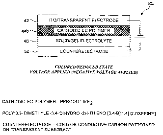
Again, the top layer is transparent electrode 42, again, preferably ITO.
The next layer is a cathodic PProDOT-Me2 EC polymer layer, which in
FIGURE 4A is shown as a transparent layer 44a, and in FIGURE 4B is shown as
a colored layer 44b. After the cathode EC polymer layer comes a solid/geI
electrolyte layer 46. The solid electrolyte layer is followed by a counter-
electrode
layer 52. No bottom transparent electrode layer is required.
Counter-electrode layer 52 is preferably gold based, platinum based, or
highly conductive carbon based, and replaces the anodic EC polymer and bottom
ITO electrode utilized in the first configuration described above. A preferred
highly conductive carbon is graphite. It should be understood that while
graphite
certainly represents a preferred highly conductive carbon, that other highly
conductive caxbon materials can also be beneficially employed as a conductive
film to be coated onto a transparent substrate to produce a counter-electrode.
Many types of conductive carbons are available from a variety of
manufacturers,
such as Tokai Carbon Co. of Tokyo, Japan; and LORESCO INTERNATIONAL,
of Hattiesburg, Mississippi. Thus the use of the term graphite herein should
be
considered to be exemplary, rather than limiting the scope of the present
invention. It is further contemplated that nickel can be beneficially employed
as a
conductive film on a transparent substrate to produce a counter-electrode. The
CA 02451615 2003-12-23
WO 03/001290 PCT/US02/20218
-18-
use of a counter-electrode can improve the speed of the color change between
states, as well as the high contrast ratio between the two states. The
counter-electrode material should be chemically stable, provide high
electrical
conductivity, and should be easy to fashion into a patterned substrate. Gold,
highly conductive carbons, and platinum have been identified as being
electrically
conductive materials that can be beneficially employed for making a
counter-electrode. It is contemplated that graphite will be very useful
because of
its low cost, and gold, while much more expensive, can be used in very thin
layers, thereby minimizing the cost of a gold based counter-electrode.
Platinum,
while electrically conductive, is likely to be so expensive as to preclude its
use. It
is further contemplated that other conductive materials can be employed to
produce the counter-electrode.
A gold based counter-electrode was produced as described below, and is
illustrated in FIGURES SA-SC. Polished float glass, 0.7rnm thick (available
from
Delta Technologies, Limited), was used as a substrate. The glass was cut into
a
4 inch diameter glass wafer 56. Lithography and sputtering techniques were
used
for forming a gold pattern 58 on the glass, wafer. Optionally, before the gold
coating was applied, a layer 60 of titanium-tungsten (TiW) was first sputtered
onto the glass substrate. TiW layers have often been used as barrier layers
and
capping layers in semiconductor manufacturing. The TiW layer helps tightly
bind
the gold layer to the glass substrate. The pattern design, or pattern
geometry,
ultimately effects the EC device. The wider the lines of conductive material
on
the counter-electrode, and the larger open areas of the patterning are
expected to
provide higher conductivity, thus enhancing the speed of the color change of
the
EC polymer, at the cost of decreasing transmittance through the counter-
electrode
when no voltage (or a positive voltage) is applied. Note that for some
applications, particularly windows, transmittance through the EC device is
very
important. If the maximum transmittance through the EC device (or through any
part of the device, such as the counter-electrode) is reduced to an
unacceptable
level, then the device may not be suitable for use ~in an application such as
a
window. The checkerboard pattern shown in FIGURES SA and SB offers a
CA 02451615 2003-12-23
WO 03/001290 PCT/US02/20218
-19-
pattern that, when sufficiently small, is substantially transparent. It is
contemplated that as an alternative to the square orifices in the gold layer,
circular
orifices or diamond shaped orifices would be equally useful, as respectively
shown in FIGURES 6A and 6B. Preferably, less than 25 percent of the glass
substrate is covered with gold, in order to maintain high transmittance. It
should
be noted that transmittance is maximized when the total area of the layer of
gold
(or graphite) is minimized, while conductivity is maximized when the area of
the
layer of gold (or graphite) is maximized. If an EC device must have excellent
transmittance, and a somewhat slower response time is acceptable, then the
percentage of the counter-electrode surface area devoted to a gold or graphite
layer can be decreased. On the other hand, if response time is more important
thaai transmittance, then the percentage of the counter-electrode area devoted
to a
gold or graphite layer can be increased. It has been empirically determined
that
covering less than 25 percent of the glass substrate with the conductive
material
represents a good compromise for EC devices that exhibit both rapid response
times and acceptable transparency.
As noted above, highly conductive carbon (such as graphite) based
counter-electrodes can also be employed. A first embodiment of a highly
conductive carbon based counter-electrode is shown in FIGURES 7A and 7B.
Once again, a preferred substrate is a polished float glass cuvette plate ,
about
0.7 mm thick. An ITO coating 64 is applied on one side of the polished float
glass cuvette plate, and a carbon coating 62 is then applied over the ITO
coating.
Preferably, the highly conductive carbon material is graphite (HITASOL
GA.66M). The electrical conductivity of this highly conductive carbon material
is
known to be not less than 10-2 S/cm. Preferably, less than 25 percent of the
glass
substrate is covered with the carbon, in order to maintain high transmittance.
While lithography and sputtering were employed for gold patterning on glass
substrate as described above, screen printing was employed for forming a
graphite
pattern on a glass substrate fox the highly conductive carbon-based
counter-electrode. It is anticipated that because screen printing technology
requires less expensive equipment than does lithography and sputtering
CA 02451615 2003-12-23
WO 03/001290 PCT/US02/20218
-20-
techniques, that mass production of highly conductive carbon-based
counter-electrodes may be less expensive than mass production of gold-based
counter-electrodes.
Note that in this embodiment of a graphite based counter-electrode, the
S glass substrate is coated with indium tin oxide on one side to form a
transparent
insulating substrate for the counter-electrode. Because the electric
conductivity of
gold is much higher than that of graphite, gold can be directly deposited on
the
glass substrate without ITO glass, but it is preferable to deposit a graphite
pattern
onto an ITO layer. While less preferred, it should be noted that an acceptable
graphite based counter-electrode can be fashioned without the ITO layer
illustrated in FIGURE 7B.
Preferably, each polymer layer within these laminated devices are on the
order of 150 nanometers in thickness, each solid electrolyte layer is
approximately
30 microns in thickness, and the gold patterned layer on the counter-electrode
is
on the order of 50-100 nanometers in thickness. A preferable range of
thickness
for a graphite layer in a counter-electrode is also 50-100 nanometers, more
preferably 100 nanometers. A preferred thickness for an ITO film is from about
10 nanometers to about 200 nanometers, with more electrical conductivity being
provided by a thicker layer. Thus electrical conductivity within an EC device
can
be manipulated by adjusting a thickness of the ITO layer, especially an ITO
layer
employed in a counter-electrode. A preferred thickness for a transparent
substrate
(such as glass or plastic) utilized in a transparent electrode (or counter-
electrode)
is about 0.5-1.0 millimeters, most preferably 0.7 millimeters.
A platinum wire has been successfully employed as a counter-electrode in
an EC device generally corresponding to the second configuration as shown in
FIGURES 4A and 4B. While EC devices having a configuration (i.e., a cathodic
EC polymer, a solid electrolyte layer, and a non EC polymer counter-electrode)
preferably employ PProDOT-Me2 as the cathodic layer, it should be understood
that other EC cathodic polymers can be beneficially employed. It should be
understood that a single polymer EC device can be fashioned using a
counter-electrode and an anodic EC polymer, as opposed to a counter-electrode
CA 02451615 2003-12-23
WO 03/001290 PCT/US02/20218
-21-
and a cathodic EC polymer. A single polymer EC device fashioned using a
counter-electrode and an anodic EC polymer would be less transparent (i.e. the
anodic EC polymer layer would be in its darker state) with no voltage (or a
positive voltage) applied, and as a negative voltage is applied to the such as
EC
device the anodic EC polymer layer would transition to its more transparent
state.
This is the opposite of a single polymer EC device fashioned using a
counter-electrode and a cathodic EC polymer, which is more transparent without
a
voltage (or a positive voltage) being applied, and become more opaque as a
negative voltage is applied.
A sample device based on the single polymer/counter-electrode EC device
described above was constructed using rectangular layers substantially 7 mm x
SO mm. An ITO coated 7 mm x 50 mm glass slide was prepared for the
transparent electrode, and a layer of PProDOT-Me2 was deposited on the ITO
coated surface. A glass wafer onto which a grid pattern of gold had been
deposited was cut into 7 mm x 50 mm plates. Similar 7 mm x 50 mm plates of
graphite deposited in a grid pattern were also prepared. A PMMA/LiC104 gel
electrolyte was uniformly placed between the cathodic EC polymer deposited on
the ITO slide and the counter-electrode to form a layered device. Two devices
were prepared, one with a gold counter-electrode, and one with a graphite
counter-electrode layer. The graphite based counter-electrode differs from the
gold based counter-electrode in that a layer of ITO was first placed on the
glass
substrate before the graphite was deposited, while no such layer was employed
in
the gold based counter-electrode. A rubber sealant was employed, and the
assembled devices were allowed to cure for about 20 hours. It is anticipated
that
additional curing time might be beneficial, and that 20-30 hours represents a
preferred range of cure times. The sealant employed was a parafilm, a readily
available, semi-transparent, flexible thermoplastic sealant. A schematic
illustration of these working models is provided in FIGURES 8A and 8B. it
should be noted that the working models are consistent with the second
embodiment discussed above with respect to FIGURES 4A and 4B. As above,
CA 02451615 2003-12-23
WO 03/001290 PCT/US02/20218
_22_
the schematic model is shown in both an oxidized state (no voltage or a
positive
voltage applied) and a reduced state (a negative voltage applied).
FIGURE 8A schematically shows a cross-sectional view and a top plan
view of a working model in an oxidized state (no voltage or positive voltage
applied). The cross-sectional view clearly shows the top layer as being
transparent electrode 42, which was prepared by coating glass slide with ITO.
Immediately adjacent to transparent electrode 42 is transparent layer 44a, a
thin
film of the cathodic PProDOT-Mez EC polymer coated onto the transparent
electrode 42. The next layer includes a generally circular solid/gel
electrolyte
layer 46, which is surrounded by a sealant 53 to prevent any of the
electrolyte
from leaking. As discussed above, the solid electrolyte layer (and sealant) is
followed by counter-electrode layer 52. Note that shape of the solid
electrolyte
layer defines that area of the EC polymer layer that will change color.
Portions of
the EC polymer layer that are not in contact with the electrolyte layer will
not
undergo a change in color. In the present example, the EC polymer layer coated
the entire generally square shaped transparent substrate, the sealant was
applied as
a generally circular mask (i.e. the sealant was applied over the entire
surface of
the EC polymer layer except for a generally circular portion where no sealant
was
applied) and the solid electrolyte layer was deposited within the generally
circular
portion defined by the sealant mask. A quite sharp demarcation between
portions
of the EC polymer immediately adjacent to the solid electrolyte layer (such
portions transitioning from a light state to a dark state under an applied
negative
voltage) was achieved relative to portions of the EC polymer layer immediately
adjacent to the sealant (i.e. not immediately adjacent to the solid
electrolyte layer,
such portions not transitioning from a light state to a dark state under an
applied
negative voltage). Very little bleed though occurred at the interface between
the
sealant and the solid electrolyte layer, enabling a sharply defined window
(i.e. the
portion of the EC polymer layer that transitioned from light to dark under an
applied negative voltage) to be achieved. Of course, the sealant mask and
electrolyte area can be combined in shapes other than the generally circular
shape
employed here. Whatever shape the sealant can be conformed into can be used to
CA 02451615 2003-12-23
WO 03/001290 PCT/US02/20218
-23-
define a window corresponding to the inverse of that shape, by filling the
inverse
(i.e. the void) with the electrolyte. Note that no bottom transparent
electrode
layer is required. FIGURE 8B shows the working model after a negative voltage
has been applied, and the portion of the EC polymer layer in contact with
electrolyte has changed color, while the balance of the EC polymer layer (i.e.
the
portion in contact with the sealant) has not. With respect to FIGURES ~A
and ~B, as noted above, the polarity of the voltage applied determines how
such
devices will respond.
Experimental Results
Electrochemical empirical studies were carried out with working samples
corresponding to the second configuration as illustrated in FIGURES 4A and 4B.
PProDOT-Mez was employed as the cathodic EC polymer, and a platinum wire
was employed as the counter-electrode. The studies were executed using an
potentiostat/galvanostat electrochemical analyzer, CH 1605A, from CH
Instruments, with silver (Ag/Ag+) as the reference electrode, an ITO-coated
one-glass slide as the working electrode, and a platinum (Pt) wire as the
counter-electrode. The electrolyte employed (in this case, a liquid
electrolyte)
was 0.1N TBAP/ACN. Spectro-electrochemistry was carried out on a Varian
Corp. UV-Vis-NIR spectrophotometer. FIGURES ~ and 9 graphically illustrate
the fast and repeatable actuation of each of the EC devices described above.
In
particular, FIGURE 9A provides switching data for an EC device with a
PProDOT-Mea cathodic layer, an electrolyte layer, and a counter-electrode
layer,
while FIGURE 9B provides switching data for an EC device with a
PProDOT-Men cathodic layer, an electrolyte layer, and a PBEDOT-NMeCz
anodic layer.
For optical switching studies, devices based on a PProDOT-Me2 cathodic
layer, an electrolyte layer, and a gold counter-electrode layer, and a
PProDOT-Me2 cathodic layer, an electrolyte layer, and a graphite
counter-electrode layer were used. Again, spectro-electrochemistry was carried
out on an UV-vis spectrophotometer. High contrast ratios in visible region
were
observed for gold based counter-electrode device, as is graphically indicated
in
CA 02451615 2003-12-23
WO 03/001290 PCT/US02/20218
-24-
FIGURE 10A. The high contrast ratios are attributed to the high transmittance
of
Au-based counter-electrode and the cathodic EC polymer in the oxidized state.
The colored state of graphite based counter-electrode device shown in
FIGURE l OB was somewhat darker than gold based counter-electrode device, but
the bleached state of the graphite based counter-electrode device was also
darker,
due to the lower percentage transmittance through the graphite based
counter-electrode layer.
Optical switching is an important characteristic of an EC device, and each
device, based on gold and graphite counter-electrodes, were tested for
switching.
FIGURE 11A graphically illustrates the results for the gold based
counter-electrode device, while FIGURE 11B graphically illustrates the results
for
the graphite-based counter-electrode device, based on absorbance under a
wavelength of 580nm and an application of 2.0V. Each device exlubited good
repeatability and a rapid change in absorbance. The percentage transmittance
in
the bleached state of the graphite based counter-electrode device was lower
than
gold based counter-electrode device, but the absorbance response to potential
is
more rapid in graphite based counter-electrode device. This result is likely
due to
the fact that graphite, whose electric conductivity is lower than that of
gold, was
patterned on ITO for enhancement of the overall conductivity.
For each device, the colors reached equilibrium within almost the same
time (less than 1 second), even at the different applied potentials, as is
graphically
indicated in FIGURE 12, with respect to the gold based counter-electrode
device.
Note that the color saturation (i.e. the degree of opacity) is dependent upon
the
magnitude of the potentials applied, as is graphically indicated in FIGURE 13,
with respect to the gold based counter-electrode device. While FIGURES 12
and 13 only refer to the gold based counter-electrode device, the graphite-
based
counter-electrode device behaved similarly.
It is believed that the redox reaction occurs just on the surface of EC
polymer film, and that the doping reaction requires very small amount of ions.
This property of the EC devices was studied using an potentiostat/galvanostat
electrochemical analyzer, CH 1605A, from CH Instruments. By connecting the
CA 02451615 2003-12-23
WO 03/001290 PCT/US02/20218
-25-
counter-electrode and the reference electrode to the above analyzer with gold
(or
graphite) patterned glass slide as a counter-electrode, electrochemical data
of an
EC polymer-deposited ITO glass slide as the working electrode were measured.
FIGURE 14A graphically illustrates the repeatability of performance during the
oxidization and reduction reactions of gold based counter-electrode device,
while
FIGURE 14B shows the same result for the graphite-based counter-electrode
device, upon varying polarity of a constant potential (i.e., 2.0 volts). Each
device
exhibited very stable repeatability within 1 second, a rapid response time.
Under
the same potential, the magnitude of the current of the graphite-based
counter-electrode device was twice that of the gold based counter-electrode.
This
result is due to the high electric conductivity of the graphite-based
counter-electrode, resulting in a color change response time that is shorter
than
that of the gold based counter-electrode device. This fact is apparent in
FIGURE 11B, where the absorbance vs. time curve of the graphite-based
counter-electrode device has a very steep slope.
Temperature dependence of the color change performance of EC materials
is also an important factor in designing EC devices. The magnitude of electric
current of EC devices under the application of constant voltage represents
color
change property of the devices.The devices (goldand graphite
based
counter-electrodes) analyzedin a Temperature&Humidity Chamber
were
(PDL-3K, ESPEC). Currenttime curves weremeasured by
a
potentiostat/galvanostat electrochemical analyzer at a constant 2.0 volts
under
various temperatures in the chamber. FIGURE 15 graphically illustrates a plot
of
the maximum electric current in each EC device as a function of temperature.
Current of the gold based counter-electrode device increased very slightly
within
a temperature range of -40 to 10° C, but it became stable in the high
temperature
range of 10-80° C, while the graphite-based counter-electrode device
was more
stable over the entire range. The maximum current change for either device was
less than 2x 10⁻³ mA from -40 to 100° C.
The speed of the switching between transparent and colored states of both
the gold based counter-electrode device and the graphite-based counter-
electrode
CA 02451615 2003-12-23
WO 03/001290 PCT/US02/20218
-26-
device is rapid, occurnng in the range of about 0.3-1.0 seconds. The
graphite-based counter-electrode device using ITO in the counter-electrode can
achieve a 0.3-0.8 second response time, upon an applied 2 volts potential, and
is
repeatable (10,000 times). That performance is faster than achieved in the
gold
based counter-electrode device (which did not use ITO in the counter-
electrode).
The gold based counter-electrode device achieved a higher percentage change in
transmittance between the transparent and opaque states. The power consumption
of the devices are modest, 2-2.5 volts times 10-20 mA. The temperature range
under which the switching is stable is a relatively wide, -40°C ~
100°C. In
addition, the weight of the devices are minimal. ~ The gold based counter-
electrode
device and the graphite-based counter-electrode device exhibit good perceived
contrast, require a low switching voltage, and hence, are of special interest
for use
in dialed-tint windows, large areas display, antiglare car rear-view mirrors,
and
other applications where controllable color switching is useful.
Specific Applications
Yet another aspect of the present invention relates to specific applications
for EC devices. In a first embodiment, an EC device including a
PBEDOT-NMeCz anodic layer is employed as a display. Because
PBEDOT-NMeCz has a yellowish tint in the oxidized state, and a blue tint in
the
reduced state, a multicolor display can be achieved. Such an EC device
preferably includes a plurality of pixels, each pixel being defined by an
individually addressable grid of a dual polymer EC device including a
PBEDOT-NMeCz anodic layer. A voltage can be applied to each pixel
individually, enabling a flat panel display to be achieved in which the color
of
each pixel is separately controlled.
Still another application specific embodiment is directed to a DW for
DNA chip reading technology based on SPR imaging with high lateral resolution.
SPR imaging is an accepted technology, which currently utilizes expensive
custom photomasks. In this embodiment, a DW including a plurality of
individually addressable pixels arranged in a grid format is employed in the
place
of the conventional photomask. The DW includes a plurality of individual
pixels,
CA 02451615 2003-12-23
WO 03/001290 PCT/US02/20218
_27_
each of which is a laminated EC such as the dual polymer and single polymer
devices described above. A voltage can be applied to each pixel individually,
enabling selective masking to be achieved, pixel by pixel. Thus a DW provides
a
switchable window, from transparent to non-transparent (dark blue) by varying
electric potential polarity. The laminated EC devices described above are
fabricated in a digital (pixel) array, whose size are typically 0.5 - 50
microns
across.
The impact of the above described DW technology is expected to be
multifold and immediately transferable to ' DNA array chip technology,
particularly the technology for reading unknown DNA and unknown molecules
(in vitro or in vivo) by using SPR. An example of using a preferred embodiment
of a DW in accord with the present invention is shown in FIGURE 16. In
FIGURE 16, a DW/SPR imaging system 100 includes a conventional SPR
imaging system in which DW 102 is inserted. Conventional elements of DW/SPR
imaging system 100 include a flow cell 104, a patterned analytic layer 106, a
gold
or silver layer 108, a laser light source 110 for directing light to the
analytic layer
along a first path 112, a first optical element 114 disposed in first light
path 112
(for polarizing the light from light source 110), a prism 116 disposed in
first light
path 112 and adjacent to the analytic layer, such that light traveling along
first
light path 112 passes through the prism. A second optical element 118 is
disposed
along a second light path 120, and a charge coupled device (CCD) detector 122
disposed in second light path 120 to receive light focused by second optical
element 118. Not separately shown are a plurality of electrical conductors
coupled to each pixel of the DW, such that a voltage can be individually
applied
to each pixel, and a power supply electrically coupled to the electrical
conductors
and the laser light source.
By combining a DW with a conventional SPR imaging systems that has
been used as a real time analyzer of unknown molecules, including DNAs and
RNAs, a new SPR system with high spatial resolution is achieved. The high
resolution DW/SPR system is expected to analyze unknown molecules and DNAs
on a real-time basis at a faster speed rate than can be achieved by
conventional
CA 02451615 2003-12-23
WO 03/001290 PCT/US02/20218
_~8_
SPR imaging systems, by scanning through one group of molecules to another by
opening the corresponding several pixels in digital window. The DW can be left
in place, and reconfigured by activating different pixels. In contrast, a
photomask
would have to be removed and replaced with a different mask to achieve a
different masking pattern.
Yet another aspect of the present invention is a smart window that can be
used in structural and architectural applications, such as in cars, planes,
and
buildings. Such a smart window is able to change state from being
substantially
transparent in a first state, with no voltage (or a positive voltage) applied,
to being
substantially opaque in a second state, with a negative voltage applied.
FIGURE 17 illustrates single or dual polymer EC devices such as those
described
above being incorporated into a conventional dual pane window 130. Note that
FIGURE 17 includes a front view, a side view, and an expanded portion view,
each of which is appropriately labeled. Smart windows differ from conventional
windows in that the EC device layered between conventional glass outer pane
134
and inner pane 136, enables wires (not separately shown) extending from the
smart Window to be coupled to a controllable voltage source, such that the
smart
window will transition from being generally transparent to being significantly
less
transparent. If a void or gap 140 separates the panes of conventional glass,
preferably the EC device is coupled to outer pane 134, rather than inner pane
136. ,
A first embodiment of a smart window is based on a dual polymer EC device
using a ProDOT-Me2 cathodic polymer layer, a solid electrolyte layer, and a
PBEDOT-NMeCz anodic polymer layer, as described above. A second
embodiment of a smart window is based on a single polymer EC device, using a
PProDOT-Me2 cathodic polymer layer, a solid electrolyte layer, and a
counter-electrode layer, substantially as described above.
Because the dual and single polymer EC devices described above exhibit
good perceived contrast and require a low switching voltage, they are
anticipated
to be of special interest in other applications as well, such as large area
displays,
automatic mirrors, and other applications where color change in response to an
applied voltage desirable.
CA 02451615 2003-12-23
WO 03/001290 PCT/US02/20218
-29-
Overview of Paired PProDOT-Me? & Counter-Electrode Functionality
PProDOT-Me2 can be used as a cathodically coloring polymer.
PProDOT-Me2 is dark blue color in its fully reduced form, and a very
transmissive light blue in its fully oxidized form. This cathodically coloring
polymer changes from a light color to a highly colored state upon charge
neutralization (i.e. reduction) of the p-doped form. The ~r ~ transition is
depleted
at the expense of transitions outside the visible region. Therefore, the
dominant
wavelength of the color is the same throughout the doping process. The EC
process of an EC device utilizing a PProDOT-Me2 cathodic layer, a gel
electrolyte
containing lithium perchlorate (LiC104), and a gold based counter-electrode is
illustrated in FIGURE 17, where the gold layer plays the role of the second
layer
required in the paired layer process explained below.
The EC process requires paired layers, with the PProDOT-Me2 layer
acting as a first one of the paired layers, and the gold based counter-
electrode
acting as a second one of the paired layers. In the left side of FIGURE 18, a
negative voltage has been applied and the PProDOT-Me2 polymer is in its
reduced, highly blue colored state. The gold based counter-electrode layer is
attracting the negatively charged perchlorate (C104) ions. In the right side
of
FIGURE 18, no voltage (or a positive voltage) is being applied. and the
PProDOT-Mez polymer is in its oxidized, p-doped light color state. The gold
based counter-electrode layer is attracting positively charged lithium (Li)
ions.
The gel electrolyte separating the PProDOT-Me2 polymer layer and the
gold based counter-electrode layer is ionically conductive but electronically
insulating, so the lithium and perchlorate ions are mobile and free to move
between the PProDOT-Me2 polymer side and the gold based counter-electrode
side under polarity change of applied potential.
The graphite based counter-electrode works by the same mechanism. This
electric double layer results in no chemical reaction, and causes no
structural
change in the counter-electrode layer (gold or graphite). The electric double
layer
can store both negative and positive charges.
CA 02451615 2003-12-23
WO 03/001290 PCT/US02/20218
-3 0-
Although the present invention has been described in connection with the
preferred form of practicing it, those of ordinary skill in the art will
understand that
many modifications can be made thereto within the scope of the claims that
follow.
Accordingly, it is not intended that the scope of the invention in any way be
limited
by the above description, but instead be determined entirely by reference to
the claims
that follow.