Note : Les descriptions sont présentées dans la langue officielle dans laquelle elles ont été soumises.
CA 02452420 2004-O1-07
1
This application is a divisional application of co-pending
application 2,105.841, filed September 9, 1993.
IMAGE AND SODND PROCESSING APPARATUS
OF THE INVENTION
The present invention relates to an image and sound
processing apparatus, and more particularly to a game computer
system processing a variety of image and sound data.
Recently, a game computer system manages plural types
of data, that is, external block and dot sequence types, and an
internal dot sequence type. Further, plural BG (background)
pictures are processed to be superimposed in the computer
system. In a conventional game computer, these data are
processed in a HSYNC or VSYNC period. Therefore, according to
the conventional system, it is difficult to process the BG data
for each block at a high speed, because a variety types of data
must be processed in the HSYNC or VSYNC period.
For example, when image data for a natural picture is
processed, a RAM is accessed for each block of the image in an
interrupt period, and an area of the RAM corresponding to dots
needed to be processed is accessed in the block accessing
period. In this case, it is sufficient to access only the dots
needed to be processed without the block access, so that the
access time is decreased. If dot accessing is realized by
forming a special circuit in the system, the circuit becomes
very large.
In the conventional computer system, the current
address of a RAM is renewed by the CPU using a predetermined
CA 02452420 2004-O1-07
2
program or an increment operation. The increment process is not
suitable for a multi-media computer such as a game computer
treating a variety of data such as graphic, video, general,
sound, etc. According to the conventional game computer, the
same data arrangement of the RAM is used for any data mode;
however, it is not effective use of the RAM.
In the conventional computer system, the background
image is managed by using a BAT (background attribute table ) and
a CG (character generator) in a VR.AM. According to the
conventional computer system, the size and position of the BAT
in the RAM are fixed, and therefore, a useless area is formed in
the RAM, because the size of the image data varies depending on
the type and kind of the data.
In game computer systems, it is necessary that the
position where the data are currently read in the memory be
monitored by ~a user program, when the data are continuously
processed. That is easy to realize if the data are read
directly; however, it is impossible to directly monitor the
current position when the RAM is accessed automatically at a
predetermined interval. In the conventional game computer, the
current position must be calculated based on the elapsed time,
and as a result, the GPU must perform much processing.
SUMMARY OF THE INVENTTON
Accordingly, it is an object of the present invention
to provide an image and sound processing apparatus in which a
CA 02452420 2004-O1-07
3
memory may be accessed at a suitable timing for any type of
data.
It is another object of the present invention to
provide an image and sound processing apparatus in which a
memory is adaptable to plural modes of data.
It is still another ob ject of the present invention to
provide an image and sound processing apparatus in which a
memory may be used effectively when plural BG (background]
pictures are superimposed therein.
It is still another object of the present invention to
provide an image and sound processing apparatus by which
continuous processing of data may be performed at a high speed.
According to a first feature of the present invention,
a memory is accessed for each dot in accordance with a first
clock signal, and is accessed for each block in accordance with
a second clock signal. The first and second clock signals are
selected to be used depending on the type of an image data to be
displayed. This processing is realized by a macro instruction
in a microprogram.
According to a second feature of the present
invention, image data are managed by different arrangements of
data in a memory depending on the data mode. An address of a
memory to be accessed is specified in accordance with a current
data mode. Specifically, the address to be accessed is
calculated in accordance with an instruction held in a register.
The register is supplied with information on initial and
CA 02452420 2004-O1-07
incremental values of the address and whether to read or write
by a microprogram, so that data access is carried out
automatically. The incremental value is calculated by a special
device.
According to a third feature of the present invention,
plural BG (background) pictures each managed by a BAT
(Background Attribute Table) in a memory are superimposed. A
start address of the BAT is held in registers, and the start
address is changed depending on the size of the BG picture.
According to a fourth feature of the present
invention, an access point in a memory is transferred from an
end address to a start address when the data at the end address
have been processed. An interrupt signal is generated when the
access point reaches the end address or an intermediate address
between the start and end addresses. A predetermined interrupt
processing is carried out in accordance with the interrupt
signal.
BRIEF DESCRIPTION OF THE DRAWINGS
24 Fig. 1 is a diagram showing operation for scanning on
a CRT display, according to a conventional computer system.
Fig. 2 is a block diagram showing the conventional
computer system.
Fig. 3 is a block diagram showing a controller chip
used in the computer system shown in Fig. 2.
Fig. 4 is a diagram showing a relation between virtual
CA 02452420 2004-O1-07
and real screens processed in the conventional computer system.
Fig . 5 is a diagram showing the configuration of a
VRAM used in the conventional computer system.
Fig. 6 is a diagram showing a relation between BAT and
5 CG shown in Fig. 5.
Fig. 7 is a diagram showing the arrangements of the
memory operating in 4, 16 and 256 color modes, according to the
conventional computer system.
Fig. 8 is a block diagram showing display processing
for BG image data according to the conventional system.
Fig. 9 is a diagram showing the data arrangement of
the BAT according to the conventional system.
Fig. 10 is a diagram showing the configuration of one
character of the BG image, according to the conventional system.
Fig. 11 is a diagram showing the configuration of the
RAM in the 4 color mode according to the conventional system.
Fig. 12 is a diagram showing the configuration of the
RAM in the 16 color mode according to the conventional system.
Fig. 13 is a diagram showing the configuration of the
RAM in the 256 color mode according to the conventional system.
Fig. 14 is a diagram showing the configuration of the
RAM in a 64K color mode according to the conventional system.
Fig. 15 is a diagram showing the configuration of the
RAM in a 16M color mode according to the conventional system.
Fig. 16 is a diagram showing display processing for
image data each having the same color, according to the
CA 02452420 2004-O1-07
6
conventional system.
Fig . 17A is a f low chart showing processing for memory
access, according to the conventional system.
Fig. 17B is a flow chart showing a process for
accessing a memory used in a computer system according to the
invention.
Fig. 18 is a diagram showing a process of sound data
according to the invention.
Fig. 19 is a diagram showing an operation for reading
the sound data from CD-ROM, according to the invention.
Fig. 20 is a timing chart showing a relation between
DCK and HSYNC signals according to the invention.
Figs. 21A, 21B and 21C are diagrams showing the
configurations of microprogram control, microprogram load
address and microprogram data registers, respectively, according
to the invention.
Fig. 21D is a diagram showing a storage area used by
the microprogram according to the invention.
Fig. 22 is a diagram showing the data arrangement of
the microprogram data register, shown in Fig. 22, according to
the invention.
Fig. 23 is a timing chart showing a relation between
operation and display periods of the microprogram according to
the invention.
Fig. 24 is a diagram showing a process for generating
address data by the microprogram according to the invention.
CA 02452420 2004-O1-07
7
Fig. 25 is a diagram showing the content of the
microprogram according to the invention.
Fig. 26 is the data arrangement of a VR.AM used in the
computer system according to the invention.
Figs. 27 to 31 are diagrams showing the arrangements
of CGs in a memory (K-RAM) operating in 4, 16, 256, 64K and 16M
color modes, respectively, according to the invention.
Fig. 32 is a diagram showing rewrite processing of a
BG screen according to the invention.
Fig. 33 is a diagram showing memory access processing
according to the invention.
Fig. 34 is a diagram showing the content of a start
address register of the K-RAM according to the invention.
Fig. 35 is a diagram showing a process for pointing an
address by the start address register according to the
invention.
Fig. 36 is a diagram showing a display example
processed by the computer system according to the invention.
Fig. 37 is the data arrangement of the K-RAM in a
single color mode according to the invention.
Fig. 38 is a diagram showing a relation between a
sound address register and an ADPCM data area according to the
invention.
Fig. 39 is a flow chart showing interrupt processing
performed at a middle point in the memory according to the
invention.
CA 02452420 2004-O1-07
DETAILED DESCRIPTION OF THE INVENTION
For better understanding of the invention, a
conventional technology will be described before describing
preferred embodiments.
In a conventional game computer, background (BG) and
sprite (SP) data are superimposed to display an image.
Fig. 1 shows a TV screen. In this screen, a scanning
line is moved left to right, and up and down. When the scanning
line reaches at the right edge, the line backs to the left edge
at a point just below the previous point in a H-blank period
(HSYNC). This process is repeated top to bottom. When the
scanning line reaches at the bottom, the line returns up to the
top in a V-blank period (VSYNC). In the H and V-blank periods,
no image is displayed on the TV screen. Generally, interrupt
operations are performed in accordance with HSYNC and VSYNC
signals, which are generated in the H and V-blank periods,
respectively. In game computers, interrupt operations are
mostly performed in the V-blank periods, because the V-blank
period is longer than the H-blank period.
In the conventional game computer, the BG data are
processed in the V-blank periods, and therefore, the access
timing of the BG data is limited.
Fig. 2 shows the conventional computer system. The
system includes a game-software recording medium 100 such as a
CD-ROM, a CPU 102 of the 32-bit type, a controller chip 104 for
mainly controlling transmission of image and sound data and
CA 02452420 2004-O1-07
9
interfacing most devices to each other, an image data extension
unit 106, an image data output unit, a sound data output unit
110, a video encoder unit I12, a VDP unit 114 and a TV display
11s.
CPU 102, controller chig 104, image data extension
unit 106 and VDP unit 114 are provided with their own memories
M-RAM, K-RAM, R-RAM and V-RAM, respectively.
Fig. 3 depicts details of the controller chip, shown
in Fig. 2. The controller chip includes an SCSI controller, a
graphic controller and a sound controller. Data supplied to the
SCSI controller is buffered in the R-RAM, which stores a variety
of data such as 8 bit data and 16 bit data. The BG data stored
in the K-RAM are supplied through the controller chip to the
video encoder. The video encoder processes image data supplied
from the controller chip and the other devices to display the
image data on the TV monitor. The video encoder operates in
accordance with display control signals VSYNC, HSYNC, DCK and
SCR ( system clock ) , the SCR being produced by the other signals .
The system clock is produced based on an "OD/-EV" signal
(odd/even field judgement signal) supplied from the video
encoder in an interlace mode.
Fig. 4 shows a virtual screen for the background
image, which is managed on a coordinate system called an "image
screen coordinate." The virtual screen is composed of 1024 x
1024 dots, that is, -512 to +512 dots in each of horizontal (X)
and vertical (Y) directions. In the virtual screen, a real
CA 02452420 2004-O1-07
screen is ensured as 256 x 244 dots. When the real screen area
is moved to up-and-down and right-and-left in the virtual
screen, the image shown in the virtual screen is scrolled on the
real screen (TV display).
5 The background and sprite images are divided into
plural character patterns and sprite patterns, respectively.
For example, each character and sprite are composed of "8 x 8"
dots and "16 x 16" dots, respectively. A position of each
character is defined by a raster and a character pitch in the
10 real screen (CRT) . That is, the background image may be defined
by the positions, colors and patterns of the characters. The
positions of the characters to be displayed are indicated on the
coordinates for the CRT.
The background image is managed by using a background
attribute table (BAT) and a character generator (CG) in the
memory (RAM), as shown in Fig. 5. The BAT includes a CG color
of 4 bits and a character code of 12 bits to specify positions
and colors of the characters to be displayed. The CG is
incorporated in the RAM for storing four actual character
patterns corresponding to CG codes in the BAT. Each character
pattern is defined by points of 8 x 8 dots and 16 colors.
The color of each character block is defined dot by
dot, and the color of each dot is defined by total bits of all
the corresponding dots on each character elements CHO to CH3 , as
shown in Fig. 6. Specifically, when the corresponding dots of
character elements CHO to CH3 are indicated by b0, b1, b2 and
CA 02452420 2004-O1-07
11
b3, a color "C" of the dot to be displayed is given by an
equation "C = b0 x 2° + b1 x 21 + b2 x 22 + b3 x 23" . It can be
considered that the color "C" may be directly treated as a color
code itsself; however, the conventional game computer uses a
color pallet which stores plural color codes to manage colors of
the background image so that many colors may be used for
displaying one background image. The color pallet is specified
in position by the color codes of the CG. The character code in
the BAT indicates the address in the CG.
In this system, the memory arrangement is changed
depending on the color mode.
Fig . 7 shows the memory arrangements. f or the 4 , 16 and
256 color modes.
In the computer system, a combination of "external
block," external dot" and "internal dot" types data are used to
form the background image.
According to the internal dot sequence type data, a
natural picture supplied from an image scanner or the like is
directly displayed by a bit-map technique. Therefore, the BAT
is not necessary for that type data.
On the other hand, the other two types of data are
image data managed by the BAT and CG in the VRAM. According to
the external block sequence type data, the CG indicates a
character pattern in the same manner as the conventional system.
According to the external dot sequence type data, the CG is used
for each dot.
CA 02452420 2004-O1-07
12
The image data generated from the three types of data
are supplied through the video encoder to the TV display, as
shown in Fig. 8.
The three types of image data are now explained.
{1) EXTERNAL BLOCK SEQUENCE TYPE
Fig. 9 shows the BA.T (background attribute table)
which is composed of a pallet bank and a character code. The
pallet bank stores data corresponding to a bank stored in the
video encoder, the pallet bank corresponding to the "CG COLOR"
shown in Fig. 5. The color pallet includes color groups each
composed of 16 colors, the color groups being selected in
accordance With data stored in the pallet bank.
The pallet bank is effective in 4 and 16 color modes
only, and other color modes are neglected. The character code
is used for specifying the CG, whereby a CG address is defined
by the character code and data held in a CG address register.
Each character pattern is defined by 64 dots of "8 x 8" by the
CG. A bits number "n" needed for displaying each dot is given
by the following equation, where colors of the number "m" are
used simultaneously to display the dot. The numbers of dots
that must be used to define a color for one dot are different
depending on the color mode.
n = Loge m
When "m" indicates 4, 16, 256, 64k or 16M, "n" becomes
2, 4, 8, 16 and 24. The RAM is arranged to be addressed by 16
CA 02452420 2004-O1-07
13
bits {= 1 word), so that 2 dots are indicated by 32 bits when "m
- 16M".
Fig. 10 shows a character matrix, where (i, j ) and "p"
represent the position (line, column) and the pallet number of
the dot, respectively.
Figs . 11, 12 and 13 show the bit structures of the RAM
in 4, 16 and 256 color modes, respectively. In accordance with
the RAM structures, the positions on the color pallet, which are
used for specifying a color to be displayed, are defined. The
color pallet has a capacity of 256 colors, so that the color
pallet may be pointed directly in the 256 color mode. In other
words, the pallet bank is not necessary in the 256 color mode.
Figs. 14 and 15 show the structures of the RAM in 64K
and 16M color modes, respectively. In these color modes, color
data are specified directly without using the color pallet. In
the 64K color mode, one dot color data are specified by YUV (Y
of 8 bits, U of 4 bits and V of 4 bits). In the 16M color mode,
two dots color data are specified by YYUV {Y of 8 bits, Y of 8
bits, U of 8 bits and V of 8 bits). The first "Y" represents
the brightness of a first dot, the second "Y" represents the
brightness of a second dot and "U" and "V represent the common
color shift of the first and second dots.
In a natural picture, colors of successive dots are
not very different from each other, and therefore, the next dots
may be separated by adjusting the brightness thereof. As a
result, character patterns may be defined by using small data.
CA 02452420 2004-O1-07
14
Specifically, the character pattern may be defined by 64 word
data, which is the same as that in 64k color mode. According to
the external dot sequence system, the conventional BG image data
may be used as they are.
(2) EXTERNAL DOT SEQUENCE TYPE
The external dot sequence process is basically equal
to the external block sequence process; however, image data are
processed dot-by-dot, not block-by-block (character-by-
character) . Therefore, only one Line in the tables shown in
Figs. 10 to 15 is used to define the CG. In the 16M color mode,
two lines are used to define two dots. The external dot
sequence process is especially useful for using the memory when
a color is continuously changed with time or with position on an
image. According to the external block sequence process, the
memory can be used effectively when most image data have the
same color.
The reason that the external dot sequence data are
necessary to display the image is now explained in conjunction
20, with Fig. 16. In a picture shown in Fig. 16, a single color is
used for showing the sky, and the color varies with time. The
64K color mode is used to display the color of the sky more
naturally. Either of the external block and external dot
sequence types data are available in this case. When the
5 external block sequence type data are used, 64 words (=1024
bytes) data must be stored in the CG, because the background is
CA 02452420 2004-O1-07
defined for each pattern of 8 x 8 dots by the CG. On the other
hand, when the external dot sequence type data are used, one
word (16 bytes) data only must be stored in the CG, because the
background is defined for each dot.
5 According to the external dot sequence type data, if
the color of the sky varies in the order of blue-white, light-
red, red, dark-red, red-purple, dark-blue, and black, seven CGs
are prepared and the character code is changed in the same
order. In this case, the external block and external dot
10 sequence types data need sizes (numbers) of CG of 64 x (CG
number) words and 2 x (CG number) words, respectively. If the
CG number is 8, the former becomes 512 words and the later
becomes 16 words . Thus, the external dot sequence type data are
useful in such a case.
15 It can be considered that the CG is used for the
external dot sequence type data instead of the color pallet,
because each CG directly specifies each color. Therefore, many
colors may be used for displaying a picture by using a small
capacity of the memory.
According to the external dot sequence type data, the
screen may be colored red when the CG is set at red in an
endless scroll mode, which is called "Chazutsu mode". In the
endless scroll mode, when the real screen is scrolled out at one
end from the virtual screen, the other end follows the one end
to be displayed continuously.
CA 02452420 2004-O1-07
16
(3) INTERNAL DOT SEQUENCE TYPE
In the internal dot sequence process, colors are
defined for each dot in the same manner as the external dot
sequence process. In the 16M color mode, two dot data may be
defined by two words of YYUV. Therefore, 16M colors can be
defined by the CG having a small capacity, and repeatability of
the image is not seriously affected by the process. The
internal dot sequence type data are especially useful for
displaying a natural picture, in which each dot of the picture
has independent color data. As mentioned before, according to
the internal dot sequence process, picture data supplied from an
external visual unit may be treated in the same manner as the
others, and therefore, the processing of the image data becomes
simple.
According to the conventional system, it is difficult
to process the BG data for each block in the HSYNC or VSYNC
period at a high speed, because the system manages not only the
external block sequence type data but also the other types of
data, and plural BG pictures are processed to be superimposed.
In the conventional computer system, the current
address of the RAM is renewed by the CPU using a predetermined
program or an increment operation.
Fig. 17A shows a flow chart for the increment
operation for the data access. For example, when the data are
accessed for each 32 blocks, the first address of the data to be
read is accessed, and then the same process is repeated by
CA 02452420 2004-O1-07
17
adding the increment value to the current address . According to
this method, continuous and interval memory access operations
are realized by adjusting the increment value.
The increment process is useful for the computer
system having a RAM of simple structure; however, it is not
suitable for a multi-media computer such as a game computer
treating a variety of data such as graphic, video, general,
sound, etc.
Especially, the increment process is not suitable for
a computer treating image data in plural modes. In this case,
it is possible that the same data arrangement of the RAM is used
for any data mode; however, it is not effective use of the RAM.
Therefore, the data arrangement in the RAM must be changed
depending on the mode in order to use the RAM effectively.
As described before, the background image is managed
by using the BAT and CG in the VR.AM. The BAT is arranged from
the first address in the VRAM, and the CG is arranged at any
region behind the BAT. According to the conventional computer
system, the size and position of the BAT in the RAM are fixed.
Therefore, a useless area is formed in the RAM, because the size
of the image data varies depending on the type and kind of the
data.
A long time ago, a sound source was generated in
accordance with waveform data, which have been generated by a
computer program based process. However, the quality of the
sound source was low. For that reason, recently, sound data
CA 02452420 2004-O1-07
18
(analog signals ) are converted into digital signals, so that the
sound waves may be synthesized by an arithmetic operation.
In game computers, a programmable sound generator
(PSG), which is small in size and has small capacity, is used.
In the PSG, wave data supplied by a CPU are modulated in
amplitude or frequency in order to generate a sound wave. The
PSG may generate simple wave to produce noise. According to the
PSG, it is easy to control the output sound; however, it is
difficult to generate a variety of sounds.
According to a pulse code modulation (PCM) method,
which is a method for A/D conversion, an analog signal is
sampled at a predetermined interval. The sampled data are
quantized, and then, are transformed to binary data to generate
digital data.
According to a difference PCM method, the difference
of the next two sampled data is quantized so that an output data
amount is reduced. Further, according to an adaptive difference
PCM method, the quantizing process is performed at a short pitch
when the next two sampled data have a great difference, and on
the other hand, the process is performed at a long pitch when
they have a small difference. Therefore, the output data are
more compressed.
The PCM and ADPCM data may be compatible with each
other by using compression and extension coefficients composed
of scale value and scale level. The sampling frequency of the
ADPCM system used for a game computer is set at approximately
CA 02452420 2004-O1-07
19
l6kHz.
In the conventional game computer, ADPCM sound data
stored in an extra recording device are read by the CPU, and the
data are extended by an ADPCM decoder in accordance with the
scale value and scale level, so that the original sound is
reproduced. The ADPCM decoder contains a synchronizing signal
generating circuit, which generates a transmission rate by using
a crystal resonator. The PCM data are reproduced in accordance
with the transmission rate.
Recently, the game computer has not only a sound
source such as PSG and ADPCM controlled by the CPU, but also an
external audio device to realize high quality sound
reproduction. For example, in a game computer using CDs
(compact disks) as recording media, a CD player is used as the
PCM sound source.
Generally, it is necessary that the position where the
data are currently read in the memory is monitored by a user
program, when the data are continuously processed. That is easy
to realize if the data are read directly for specifying the
address to be accessed. However, it is impossible to directly
monitor the position where the ADPCM data are currently read to,
because the RAM is accessed automatically at a predetermined
interval. For that reason, the current position must be
calculated based on the elapsed time, and therefore, the CPU
must perform mush processing. As a result, the computer can not
operate at a high speed.
CA 02452420 2004-O1-07
Fig. 18 shows a sound reproducing system of the
invention. In this system, sound data registered in a CD-ROM
are read by a predetermined chip containing SCSI and
controllers, and the read data are stored in an ADPCM area of
5 the K-RAM. The sound data are transmitted to a sound
reproducing chip (sound box) at a predetermined timing, and the
sound data are reproduced to be supplied from a speaker.
The sound data may not be always wholly stored in the
K-RAM because of the capacity limitation of the K-RAM. For that
10 reason, the following sound data are stored in a data area where
the previous data have been reproduced, as shown in Fig. 19. If
all the following sound data are stored in the K-RAM after the
previous sound data have been reproduced completely, output
sound data are broken at some intervals.
15 According to the invention, hardware is structured to
perform interrupt processing at a check point which is
determined by a program. In a ring mode, in which the access
point of the RAM is transferred from the end to start addresses
for continuous reproducing, the interrupt processing is
20 performed when the access point reaches an intermediate (middle)
or the end address. Specifically, the first and last halves
data are rewritten when the access point reaches the
intermediate and end addresses, respectively, so that continuous
reproducing is realized. In interrupt processing, the following
data are written in the reproduced area of the RAM.
In this invention, an arithmetic process for accessing
CA 02452420 2004-O1-07
21
the K-RAM is programmed in the controller chip whereby a user
may select access timing by using a register. VSYNC, HSYNC and
DCK (dot clock) signals may be used as control signals.
Fig. 20 shows a time relation between the HSYN and
DCK, the DCK of about 341 cycles being included in one HSYNC
period. The RAM is accessed in accordance with the dot clock
signal. A microprogram is loaded into a controller chip at a
location specified in a microprogram load address register.
When an initial address is specified in the register, the
microprogram begins to be loaded. It is necessary that an MPSW
in a microprogram control register be set at "0". After the
loading of the microprogram, the microprogram begins operating
when the MPSW is set at "1". A microprogram data register
specifies which cycle is used for the access.
Figs. 21A, 21B and 21C show the configurations of the
microprogram control, microprogram load address and microprogram
data registers, respectively.
Fig. 22 shows an actual configuration of the
microprogram data register. The microprogram data register
holds an access address of the K-RAM, the timing for generating
the address, and the direction to which read data are
transmitted.
According to the external block and external dot
sequence types data, the BAT data are read first, and then the
CG data are read using two dots. Description data are divided
into two blocks (A bus and B bus), the following contents being
CA 02452420 2004-O1-07
22
included in the data.
(1) process / non-process (NOP / -NOP)
(2) BG screen number (0 to 3)
(3) rotation / non-rotation
(4) BAT / CG (BAT / -CG)
(5) BAT indirect CG / direct CG (indirect / -direct CG)
(6) CG offset
The controller chip supplies BG screen data for each
dot in synchronization with HDISP (horizontal display period).
On the other hand, the microprogram operation is started and
ended in synchronization with BGDISP (BG display period).
As shown in Fig. 23, the rotation process and non
rotation process have different delay times, so that non
rotation and rotation screens are processed in synchronization
with BGNDISP and BGRDISP, respectively. Therefore, the
microprogram operates in a MICRO.P period.
The graphic controller chip may manage five modes of
4, 16, 256, 64K and 16M color for each BG image, that is, the
image data in the different color modes can be displayed
simultaneously. Operation in 8-dot clock cycle is written in
the two K-BUS units independently in accordance with the
microprogram, so that the buses operate step by step
independently and such that 8-dot clock cycle is repeated.
Fig. 24 shows a timing table for an address generating
CA 02452420 2004-O1-07
23
timing by the microprogram, the example being for a triple
screen mode as shown below. Fig. 25 shows an example of the
contents of the microprogram.
(1) BGO : 256-color mode of external block sequence type
(2) BG1 : 16-color mode of external block sequence type
(3) BG2 : 16-color mode of internal dot sequence type
B-bus data are specified by "BGO indirect CG (0)" in
the 0 cycle, so that "external block sequence type 256 color
mode BAT indirect CGO" is accessed in a BRAM. At this time an
ARAM is not accessed, that is NOP (non-operation) is carried out
in the ARAM.
According to the conventional system, the BG data are
accessed during an interrupt period of video control signals,
the access processing being performed for each character. If a
variety of types of imaged data are managed by the conventional
way, the system needs a very large electric circuit.
On the other hand, according to the invention, the BG
data are accessed for each dot in accordance with a user program
(microprogram), therefore, the RAM may be accessed effectively
at a high speed.
Fig. 26 shows the configuration of the VRAM, in which
a part corresponds to the diagram show in Fig. 5. The
background image is managed by using a background attribute
table ( BAT ) and a character generator ( CG ) in the memory ( VR.AM ) .
CA 02452420 2004-O1-07
24
The length (bits) of the CG varies depending on the color mode.
That is, the CG is composed of 2 and 4 bits in the 4 and 16
color modes, respectively.
Figs. 27 to 31 show the memory arrangements in the 4,
16, 256, 64K and 16M color modes, respectively.
Operation of the address calculating instruction will
be explained, where a first line data of BG pictures each
composed of 8 x 8 dots characters is changed. The BG pictures
are arranged 32 x 32 dots on a screen, as shown in Fig. 32.
There are three types of registers RegOC (for
writing), RegOD (for reading) and RegOE (RAM access selection),
these registers being used for memory access operation. The
RegOD is set as follows to rewrite data stored in the first line
of the BG screens
Writing address (bit 0 to 17) : Initial address
Offset (bit 18 to 23) . 32
The offset can be set in a range between -512 to +512,
the "+" and "-" representing increasing and decreasing,
respectively. In the above example, the offset is set at +32
(bits) so that BG data are rewritten at an interval of 32 bits.
Such address calculation is carried out by a BG processing unit .
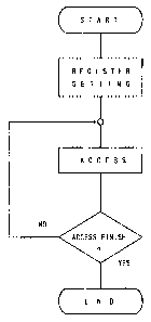
As shown in the flow chart of Fig. 17B, when an access
instruction is provided, the next access address is
automatically calculated by the BG processing unit. Therefore,
desired data processing may be carried out automatically as long
as access instructions are provided continuously.
CA 02452420 2004-O1-07
Fig. 33 shows memory access operation when the access
instructions are carried out continuously. The BG processing
unit includes two memories K-RAM#A and K-RAM#B, which are
established in accordance with on/off of bit-17 in the writing
5 address.
In this embodiment, image data are processed in 4, 16,
256, 64K and 16M color modes. An increment value of an address
to be accessed is different depending on the color mode, when
the image data are processed at a predetermined interval. When
10 an area composed of continuous dots is processed, the offset is
set at "1".
According to the embodiment, the start address and
offset values are established in advance so that the address
calculations are carried out by the system for the display mode.
15 The increment processing is carried out by the hardware at a
high speed, and therefore, the program becomes simple, and a
debugging operation may be performed easily. Especially, the
method is useful for graphic processing, in which display areas
are regularly renewed.
20 The controller chip is provided with K-RAM start
address and display size registers for specifying a start
address of the BAT in the K-RAM and a display size,
respectively. The K-RAM start address register holds BAT and CG
addresses, as shown in Fig. 34.
25 In this embodiment, the BG image data include main and
sub-pictures. The main picture is displayed on the sub-picture.
CA 02452420 2004-O1-07
26
In the BGO picture, each of the BAT and CG has its own address
register so that the main and sub-pictures are managed
independently. Each BGO picture has four address registers. In
the BG1 to BG3 pictures, the BAT and CG have one address
register so that each of the main and sub-pictures has one
register. The K-RAM includes an ARAM and a BRAM. The ARAM and
BRAM are selected when A/B = 0 and A/B = 1, respectively. In
the address register, "-A/B" at the seventh bit indicates
whether the ARAM or BRAM is selected.
Fig. 39 shows a relation between a BAT/CG address
register and the K-RAM. An address of the BAT is defined by
figures at the last seven bits and ten bits of zero in the BAT
register. An address of the CG is given as follows in
accordance with the color modes:
[4 COLOR MODE]
00 <character code> 000 + <CG address> 0000000000
[16 COLOR MODE]
0 <character code> 0000 + <CG address> 0000000000
[256, 64R and 16M COLOR MODES]
<character code> 00000 + <CG address> 0000000000
In these formulas, <character code> indicates the
content of the BAT and <CG address> indicates the last seven
bits of the CG address register. In the character codes, the
end bit is set at "0" in the 256 color mode and the end two bits
are set at "00" in the 64K and 16M color modes. Therefore, as
long as the CG addresses are different from each other,
CA 02452420 2004-O1-07
27
different types of the CG may be obtained even though the same
BATs are stored in the RAM.
The address registers are sampled for each raster, and
are effective from the following HSYNC (HSYNC : a non display
period in that a scanning line moves from left to right and
returned to the left).
Fig. 36 shows an example of the background image, in
which a screen is divided into two of upper and lower regions.
According to the conventional BAT, two CGs for the
lower and upper regions are required to form the picture in this
case, because the conventional BAT treats continuous regions
only. The CGs may be arranged to be linked to each other or
separated by some space . The picture is displayed only by a
continuous process of the BAT. A lower half character code of
the BAT must be changed to the CG of the following picture in
order to change the lower picture only. This process takes a
long time, and therefore, the upper and lower pictures can not
be displayed separately quickly.
According to the preferred embodiment, the upper and
lower pictures are stored in BAT1 and BAT2 separately. The
locations of the BAT1 and BAT2 are not limited in the K-RAM.
The K-RAM includes upper and lower CGs corresponding to the BAT1
and BAT2, respectively. In order to display the upper and lower
pictures independently, the BAT address register is set at an
address of the BAT1 at first, and then the set address is
changed to an address of the BAT2 (BAT1), because an address in
CA 02452420 2004-O1-07
28
the BAT address register is effective before the following
HSYNC. If only the upper picture is changed, another BAT is
prepared in the K-RAM, and the BAT address is changed.
According to the conventional system, which does not
use the BAT address register, it is impossible for two operators
to play a game using the upper and lower screens separately.
The BAT and CG address registers may be used to
display a screen whose color changes from red through blue to
yellow throughout. This process is carried out in the endless
scroll mode (Chazutsu mode). When a KRAM, shown at the left in
Fig. 37, storing three pairs of BAT and CG is used, a BAT
address is changed in the VSYNC period. On the other hand, when
a KRAM, shown at the right in Fig. 37, storing a single bat and
plural CGs is used, a CG address is changed in the VSYNC period.
In these cases, one word (16 bits) and two words are sufficient
for the BAT and CG, respectively, even in the 16M color mode.
According to the invention, only the required BAT area
is used, so that the memory may be used effectively. Further,
the screen may be easily divided in a horizontal direction,
because the BAT address register is effective in the HSYNC
period.
Fig. 38 shows an ADPCM data area in the KRAM. In the
sound controller, a check point where interrupt processing is
carried out from is specified by a sound half address register.
The sound half address register includes #1 and #2 registers for
channels one and two. Now considering the case using channel
CA 02452420 2004-O1-07
29
one only, whether the interrupt processing is carried out is
controlled by a sound buffer control register #1. When the
interrupt processing is carried out at middle and end points "m"
and "e", the sound buffer control register has the following
modes.
RING BUF = 1 (RING BUFFER MODE)
BUF END = 1 (INTERRUPT AT END POINT)
BUF HALF = 1 (INTERRUPT AT MIDDLE POINT)
In the ring buffer mode, when the sound data at the
end point are read, the sound data at the start point are
automatically read again. The start and end points are
specified by sound start address and sound end address
registers, respectively. The sound half address register #1
holds the middle point address of the ADPCM data.
In this case, when interrupt processing is carried out
at the point "m", the following data are written in an area "A"
where the previous data have already been processed, as shown in
Fig. 39. When interrupt processing is carried out at point "e",
the following data are written in an area "B" where the previous
data have already been processed.
In Fig. 39, "processing" includes processes for
preparing display of image, generating sound in the sound box,
transmitting sound data from the K-RAM, and the like. These
processes are set in registers so that the processes are carried
out automatically without a user program. The interrupt
processing at the middle and end points begin automatically by
CA 02452420 2004-O1-07
the system using the sound registers; however, interrupt
processing must be carried out by user.
According to the invention, a position where the
processing is currently running is not required by the user
5 program during other processing, and therefore, the computer
system may work at a high speed. The effect is especially
remarkable for long time sound reproduction.