Note : Les descriptions sont présentées dans la langue officielle dans laquelle elles ont été soumises.
CA 02452694 2003-12-29
WO 03/003079 PCT/N002/00238
APPARATUS AND METHOD FOR PRODUCING FIBRE BRAGG GRATINGS IN A
WAVEGUIDE.
This invention relates to an apparatus and a method for
fabrication of optical waveguide Bragg gratings and the use
of diffraction gratings in such fabrication.
Waveguide Bragg gratings are popular components used
as wavelength selective filters in fiber-optic communication
systems [1]. They are also popular for fiber-optic sensors
because of their small size combined with the sensitivity of
their reflection or transmission properties (typically the
peak reflection wavelength) to strain, temperature and other
mechanisms that change the fiber refractive index [2].
Fiber Bragg gratings (FBG) consist of a periodic
modulation of the refractive index in the core (or more
precisely within the modefield cross section) of an optical
fiber [3]. The period of this modulation equals AB=AB/2n
where n is the fiber refractive index and AB is the optical
Bragg wavelength at which the local reflectivity has its
maximum. The index modulation is usually produced by
illuminating the fiber core with ultraviolet (UV) light from
a laser with wavelength Auv in the range from 190 to 300 nm
and with a spatial intensity modulation period AIF=AB.
Typically, a frequency doubled Argon ion laser with
wavelength AUv-_244 nm may be used.
The intensity modulation can be created by splitting
the laser beam and recombining the beams on the fiber via a
mirror [4, 5] or lens [6] arrangement at an angle UFiber-
2aresin(AW/n=F). The UV beamsplitter can either be formed by
a semitransparent mirror, a diffractive phase mask
(spatially modulating the UV phase), or an amplitude mask
(spatially modulating the UV amplitude). The angular
separation between the +1 and -1 order diffracted beams from
such a mask equals aMask=2aresin (Aov/AMask) , where AMask is the
mask period at the position where the mask is illuminated.
It is also possible to produce gratings by placing the
fiber in the near field behind a diffractive mask where
diffractive orders still overlap. However, there are dis-
advantages with the near field approach. First, the zero and
CA 02452694 2003-12-29
WO 03/003079 PCT/N002/00238
2
higher order diffracted beams from available non-ideal masks
will cause an unwanted background exposure which limits the
available index modulation amplitude in a fiber with a
limited photoinduced index change. Second, nonlinearities in
the photosensitivity (index change versus UV exposure
energy) at high exposure levels may induce background index
variations due to the mixing of three or more diffractive
orders. These background index changes will depend on the
relative phases of the mixed beams within the fiber, and it
will therefore depend on variations in the distance between
the fiber and the phase mask in the order of A1F. In practice
it is very hard to avoid that the distance varies by many
AIF, hence the resulting background index variations will
cause errors in the effective grating phase seen by light
propagating along the fiber waveguide. A third problem
arises if one wants to use scanning techniques where a small
diameter UV beam is scanned across the fiber and mask to
enable spatially dependent modulation of the grating phase
and amplitude by moving and dithering the mask during the
scan, as suggested in [7]. In this configuration (and also
in the scanning fiber technique [8] discussed in more detail
below) the fiber must be placed very close to the mask
(typically at a distance of 100-300 pm) to ensure overlap
between the +1 and -1 order diffracted beams. The need for
such a small spacing induces a high risk of damaging the
delicate mask surface, as well as potential problems with
static electric forces between the fiber and the mask, as
discussed in [6].
Various stepwise grating exposure techniques have been
disclosed. Two similar systems are disclosed in [8, 9],
where the fiber is moved through a stationary UV
interference pattern in the direction parallel to the fiber
axis while short pulses are fired from the UV source at
regular intervals when the phase of the UV intensity pattern
relative to the fiber matches the wanted index modulation
phase. A disadvantage of this pulsed technique is that the
duty-cycle of the pulsing UV source must be low, preferably
<20-30 % in [8] and even lower in [9], to enable high
visibility of the exposure and thus low background index
CA 02452694 2003-12-29
WO 03/003079 PCT/N002/00238
3
change. With limited peak UV intensity available, for
instance due to limited source power available or to damage
limitations of the fiber or the UV optics, this will cause
significantly longer production times compared to approaches
using continuous exposure. Short writing time per FBG is
generally advantageous, since it minimizes grating errors
caused by slow drift in the relative positions of components
in the FBG production system.
An alternative version of the step writing technique
where the UV source is operated in a continuous wave mode is
disclosed in [4]. In this approach the interference fringes
are moved at the same speed as the fiber by moving the
diffractive mask, but the mask position is reset each time
the fiber has moved some multiple of Bragg periods. This
technique can allow for shorter writing times than the
techniques described in [8, 9].
A potential problem with the step writing techniques is
that the periodic pulsing of the UV source or the resetting
of the mask will tend to cause a super periodic modulation
of the grating strength and/or phase with a super period
length that corresponds to the pulse or resetting period. If
the resetting period equals MLB where M is an integer, this
will cause grating sideband reflections at wavelengths that
correspond to Bragg wave numbers which are separated from
the nominal Bragg wave number 2p/LB by integers of 2p/(MLB).
There are two reasons why M preferably should be a small
number. First, the sideband separation can usually be made
so large by increasing M that the sidebands do not cause any
problem for the FBG applications of interest. Second, as
discussed in [9] the strength of the sideband reflections
will be reduced when M is reduced due to averaging. This is
because the number of step exposures at each position on the
fiber is increased.
In the mask stepping approach, maximizing the speed and
accuracy by which the mask position is reset will also
contribute to minimize the super periodic modulation and the
grating sideband reflectivity. In order to minimize M and to
maximize the resetting speed it is thus desirable that the
fringe position can be modulated with a large bandwidth.
CA 02452694 2003-12-29
WO 03/003079 PCT/N002/00238
4
This may limit the size of the mask, as the mechanical
resonance frequencies are typically inversely proportional
to the size of the modulated device (the mask).
It is possible with the step writing techniques to
impose discrete phase-shifts in the index modulation by
suddenly changing the phase of the interference fringes as
the fiber is scanned through the UV spot. The fiber section
that is illuminated by the UV spot when the fringe phase
changes will in this case be partially exposed with both
fringe phases, and the grating phase-shift will thus occur
gradually across this section. Apodization of the grating
strength can be implemented without perturbing the grating
phase or the mean exposure per grating period by modulating
the phase of the fringes relative to the fiber while the
fiber is scanned through the UV spot, without perturbing the
mean phase value.
It is also possible to stretch or compress the Bragg
period nB slightly relative to the UV interference period
AIF=Xov sin ((XFib~r/2 ) by gradually changing the fringe phase
relative to the fiber as the UV spot is scanned along the
fiber. The Bragg wavelength shift achievable by this method
is limited to about L1Ag,max AIF2/ (4Lspot) where Lspot is the 3dB
UV interference spot size [5]. When the shift increases
above this limit the visibility of the integrated exposure
decreases substantially because the fringe phase exposed to
each fiber position varies significantly when the fiber
moves through the UV spot. With typical numbers Lspot=0.lmm,
AB=1550nm, and n=1. 465 we have LAB,max=2~1s2/ (4nLspot) =2 = lnm.
Gratings covering bandwidths larger than 2,nAg,max cannot be
exposed in a single scan with the prior art step writing
techniques.
Multi-channel gratings [10) are promising devices both
for telecommunication and sensor applications employing
wavelength division multiplexing (WDM), as they comprise the
functionality of a number of single gratings into one
grating making a more compact device. The index modulation
of a multi-channel grating with N Bragg wavelength can be
modeled as
CA 02452694 2003-12-29
WO 03/003079 PCT/N002/00238
N
On = Ano y, cos.2;c(1I ABO +1 / Ap +Oi)
i=1
where ano is the index modulation amplitude of each
subgrating, 2n/A130 is the Bragg wavenumber offset, 2rn/Z1P is
the Bragg wavenumber channel spacing, and cpi is the phase of
sub-grating i. An is periodic with period A. If the phases
5 cgi of all subgratings are equal, the peak-to-peak index modu-
lation will equal Onpp = 2NAno, as illustrated by curve C in
Fig. 1 for the case N 16. As the available index change in
photosensitive fibers is limited, it may be advantageous to
minimize AnpP. For large values of N the value of Anpp can be
reduced to the order of 2~NAno by carefully selecting the
phases cpi as shown in [11]. Numerical calculations indicate
that Anpp can be reduced to (2J+1.5)AjZa or less for N > 4, as
illustrated for N = 16 by curve A in Fig. 1. It is therefore
of interest to find a method for writing multi-channel
gratings where the subgrating phase relationship can be
accurately controlled. Also in multi-wavelength fiber Bragg
lasers, proper control with the relative phase the grating
channels is of importance [12].
The step-writing method described above allows
arbitrary multi-channel gratings to be produced in a single
writing operation. However, the total number of channels
must be confined within the available bandwidth of 2AAB,max=
It is also possible to write multi-channel gratings
sequentially, inscribing one channel at the time. If the
total bandwidth covered by the channels exceeds 2AAg,max the
UV interference period AIF needs to be changed between each
writing cycle. This can be accomplished by replacing the
diffractive mask and/or tuning the interferometer mirror or
lens positions, possibly combined with a tilting of the
mirror axis. The distance between the fiber and the
diffractive mask may also have to be adjusted to ensure
proper overlap of the interfering beams at the fiber. In
this replacement and readjustment process the task of
maintaining control with the relative phases of the
different subgrating exposures is very difficult.
CA 02452694 2003-12-29
WO 03/003079 PCT/N002/00238
6
A method will be described in the following for
ensuring control of the relative phase of the different
subgratings during such sequential exposures. However, each
writing cycle will always contribute with a mean index of
Lno, and the total index modulation including background
index will therefore at least be in the order of
(N+-~N+0.75)Ano , as illustrated by curve B in Fig. 1. The only
way to avoid a background index in the order of Nno is by
inscribing all Bragg wavenumbers grating in a single
exposure.
If the step-writing methods described above are used to
produce multi-channel gratings covering a large bandwidth
(>20nm), the UV spot size Lspot would need to be extremely
small (at least <20pm). It is possible to focus I7V laser
beams extremely tight. However, because the UV intensity
must not exceed the damage threshold of the fiber, the time
required to write a single grating may become unacceptably
long.
It is a first objective of the present invention to
provide an easy and accurate method and a device for
adjusting the interference period AB in an optical waveguide
Bragg grating production facility over a wide range, thus
allowing the facility to easily produce a wide range of
Bragg wavelengths in a flexible way.
A second objective is to provide a method and device
for varying AB during the grating exposure while maintaining
accurate control with the phase of the exposed pattern
during the exposure.
A third objective is to provide a practical method and
device for writing large bandwidth multiple channel optical
waveguide gratings with high spatial resolution super-
periodically modulated grating profile with (a close to)
optimum utilization of the available refractive index
change, which does not require focusing of the laser beam
down to a spot size that is comparable to or smaller than
the wanted spatial resolution.
A fourth objective is to provide a practical method and
device for writing multiple channel optical waveguide
gratings with high spatial resolution superperiodically
CA 02452694 2008-03-05
7
modulated grating profile, which only requires a diffractive
mask that is slightly longer than one superperiod length
plus the UV interference spot size.
A fifth objective is to provide a fast and effective
method for writing waveguide gratings with a step exposure
technique with a short stepping period, which maximizes the
strength of the grating and minimizes the amplitude of
unwanted grating, which does not require high bandwidth
modulation of the phase mask position, or put limitations on
the size of the phase mask that can be used.
According to an aspect of the present invention there
is provided optical waveguide Bragg grating fabrication
apparatus comprising:
a light source means providing a beam of ultra violet
(UV) light;
optical means for adapting the light beam to form an
interference pattern in a photo sensitive optical
waveguide, the interference pattern having a spatial
intensity modulation along the length of the optical
waveguide and thus providing an optical grating in the
waveguide in the form of a refractive index modulation,
wherein the optical means comprises a first position
control means;
a waveguide holder assembly comprising a second position
control means for setting the position of the optical
waveguide, the optical means comprises a movable non-
uniform diffractive mask for dividing the optical beam in
at least two beams, the diffractive mask comprising a
section with super periodic patterns, the superperiodic
pattern comprising repeated segments of arbitrarily
modulated periodic index variation, each segment forming
one period of the super-periodic pattern; and
optical elements for collecting two or more of the light
beams to interfere on the optical waveguide.
CA 02452694 2008-03-05
7a
According to another aspect of the present invention
there is provided a method of fabricating an optical
waveguide grating comprising the steps of:
providing a beam of light using an ultraviolet (UV) light
source;
directing the UV beam through optical means for providing
an interference pattern in a photosensitive optical
waveguide;
altering and determining the position of at least part of
the optical means relative to the, UV beams using a first
position control means;
altering and determining the position of an optical
waveguide holder assembly using a second position control
means, the optical waveguide holder assembly comprising the
at least one optical waveguide; and
controlling the position of a non-uniform superperiodic
diffractive mask being part of the optical means, thereby
controlling which area of the mask is exposed to the UV
beam, and thus yielding an interference pattern in the
waveguide corresponding to that part of the diffractive
mask which is exposed to the UV beam.
The invention will now be explained in further detail
with reference to the accompanying drawings wherein
Fig. 1 shows the index modulation range (maximum and
minimum within one super-period A. of an N=16
channel optical waveguide Bragg grating.
Fig. 2A shows the UV interferometer configuration where
the UV beams are recombined using lenses.
Fig. 2B shows the UV interferometer configuration where
the UV beams are recombined using mirrors in a
Talbot geometry.
Fig. 2C shows the UV interferometer configuration where
the UV beams are recombined using mirrors in a
quasi-Sagnac configuration.
Fig. 3 illustrates a diffractive mask with a super-
periodic mask pattern.
CA 02452694 2008-03-05
7b
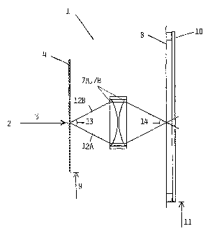
A preferred implementation of the apparatus and method
is illustrated in Fig. 2A. An ultraviolet (UV) source 2
provides a beam-3 of UV light. The beam of light falls on
otical means 4,7A,7B,9 for adapting the light beam to form
an interference pattern in a photosensitive optical
waveguide B. More specifically, the beam 3 of W light is
first transmitted through a diffractive mask 4 where the
beam is divided in mainly two diffracted beams 12A,12B,
where one beam 12A is a +1 order diffracted beam and the
other beam 12B is a.-1 order diffracted beam. The two beams
12A,12B are directed away from the diffractive mask at
CA 02452694 2003-12-29
WO 03/003079 PCT/N002/00238
8
directions differing by an angle aMask 13. The two beams
12A,12B are recombined by two cylinder lenses 7A,7B mounted
in a lens holder to create an interference pattern on the
waveguide 8. The two beams recombine at an angle O(waveguide 14
with respect to each other. The position of the waveguide 8
and the waveguide holder 10 is movable in the direction
parallel with the waveguide. When this waveguide and the
waveguide holder is moved, the waveguide is scanned through
the interference fringe pattern. The illuminated region on
the diffractive mask 4 can be varied by moving the mask
position XMask= In this description the term waveguide is
intended as a general term, including optical fibers,
waveguides in integrated structures, and other commonly
known guides for optical light.
Separate laser interferometers are used to measure the
position of the waveguide Xwaveguide and the mask XMask (relative
to the substrate onto which the lens actuator is mounted,
see below) with a precision that is significantly better
than one Bragg period.
The diffractive mask 4 comprises a non-uniformity in a
direction parallel with the longitudinal axis of the
waveguide 8. A non-uniform grating is written in the
waveguide 8 by imaging the pattern on the illuminated part
of the mask 4 onto the waveguide 8.
The diffractive mask 4 can be moved along a direction
of the non-uniformity, that is, along a direction of the
non-uniformity which is imaged onto the waveguide in a
direction parallel with the longitudinal axis of the
waveguide. The direction of the non-uniformity can be
denoted the x-direction.
The position of the fringes in the interference pattern
of the UV radiation which writes the grating in the
waveguide can be controlled by position control means 9. The
position of these fringes is typically controlled within an
accuracy better than the typical Bragg period.
In a preferable embodiment of the invention these
position control means 9 control the position of the
diffractive mask 4, preferably with an accuracy better than
a period of the interference pattern. The position control
CA 02452694 2003-12-29
WO 03/003079 PCT/N002/00238
9
means may also comprise means for controlling the position
of one or more lenses 7A-B and/or mirrors 5A-B,6A-B which
form a part of the optical means. In a further preferred
embodiment of the invention the first position control means
9 is adapted to move an optical mirror 5A,5B or a lens 7A,7B
in a direction substantially parallel with the surface of
the phase mask 4 or the longitudinal direction of the
waveguide 8. In order to control the phase of the
interference fringes within time intervals corresponding to
a waveguide movement of less than a few Bragg periods the
position of one or more of the lenses or mirrors can be
modulated with a large bandwidth.
Alternative implementations employing mirrors instead
of lenses are illustrated in Fig. 2B with a Talbot
interferometer. In this case the two diffracted beams
12A,12B coming from the diffractive mask 4 are combined by
mirrors 5A,5B in the path of each beam. In Fig. 2C a version
of the invention using a quasi Sagnac interferometer is
shown. In this case the two diffracted beams 12A,12B being
formed by the diffractive mask 4 are first transmitted
through the waveguide and the waveguide holder assembly. The.
first beam impinges first on one mirror 6A which directs the
beam onto the other mirror 6B which directs the beam back
towards the waveguide. The other beam impinges first on one
mirror 6B which directs the beam onto mirror 6A which then
directs this other beam back towards the waveguide. The two
beams are thus made to combine in the region of the
waveguide.
In these implementations the phase of the interference
fringes may also be controlled by moving or tilting one or
both mirrors 5A-B,6A-B, possibly with a piezoelectric
actuator. In all three illustrated interferometer designs it
is also possible to control the interferometer phase by
controlling (not only measuring) XWaveguide or Xmask very
accurately.
High speed resetting of the interference phase for the step
writing technique may, though, be easier to implement by
moving the lenses/mirrors which usually can have smaller
dimensions than the waveguide 8 and the mask 4. The phase
CA 02452694 2003-12-29
WO 03/003079 PCT/N002/00238
can also be adjusted by other types of modulators, like
electro-optic, thermo-optic, or stress-optic, strain-optic
devices.
A preferred embodiment of the invention comprises reset
5 means for rapidly resetting the position of one or more
lenses, mirrors or glass prisms and/or the angle of one or
more mirrors which is controlled by the position control
means 9, for example at given time intervals, in order to
limit the maximum displacement of the envelope of the
10 interference pattern to only one or a limited number of
Bragg periods between each reset operation.
High speed phase control may not be required if step
writing is implemented by pulsing of the UV source 2. In one
preferred embodiment of the invention, the light source
means 2 comprises means for reducing the intensity of or
switching off the light source, in particular for switching
the light source off during a reset operation. In such a way
a reduction in the time averaged fringe contrast due to the
varying phase during the resetting operation-is avoided.
Further, the use of such an intensity modulation in addition
relaxes the requirements on the speed of the reset
operation, thus yielding a possibility of writing with a
somewhat higher speed along the waveguide for a given
bandwidth of the modulator that is to perform the resetting
of the fringe position. Such an intensity modulator could
also be arranged in combination with a phase modulator.
In a first preferred implementation the phase mask has
a non-uniformity comprising a variation in the amplitude,
period or phase of the pattern.
The phase mask period AMask can be continuously chirped
or step-wise chirped in the x-direction. In one version the
mask can be linearly chirped. The Bragg wavelength can thus
be changed during the writing process by moving the phase
mask.
A more complex mask can be as illustrated in Figure 3
where a diffractive mask 4 having one or more sections SN,
each section characterized by its super-periodic pattern.
The super-periodic pattern of each section may consist of
repeated equal segments SPM of a periodic index variation,
CA 02452694 2003-12-29
WO 03/003079 PCT/N002/00238
11
the length of each segment corresponding to one super-
period, A. The super-period may be an arbitrarily modulated
index variation.
A spatially varying (non-uniform) diffraction pattern
is inscribed in the diffractive mask. The period AMask of the
mask pattern can be varied or chirped in the x-direction.
The period AB inscribed in the waveguide can thus be selected
simply by changing XMask= Curved lenses should preferably be
used for focusing of the beams inside the interferometer.
This ensures that the overlap of the two beams at the
waveguide remains unchanged when aMask and aWaveguide vary, as
opposed to the situation if glass prisms are used instead of
lenses. Similarly, curved focusing mirrors should preferably
be used in the interferometers of Fig. 2B and 2C. If no
curved optics is used it may be necessary to vary the
spacing between the mask and the waveguide to ensure overlap
at the waveguide of the UV beams. This could in principle be
achieved by tilting the mask slightly relative to the x-
axis. One or more of the lenses could be Fresnel-type
lenses.
Sequential writing of multiple Bragg wavelengths into
the same waveguide section can be achieved by moving the
diffractive mask 4 to a position with a different period AMask
between each writing sequence. Provided that the diffractive
grating phase distribution along the mask is known, the
relative phase of the overlaid gratings can be controlled by
measuring the exact XMask and XWaveguide and controlling the lens
position accordingly.
Continuous chirping of the Bragg period along the wave-
guide can be achieved by moving the chirped mask
continuously during the exposure. The speed of the fringe
phase modulation (for step writing) must then be increased
or decreased, depending on the speed and direction of the
mask, to compensate for the phase mask movement.
It was mentioned in the prior art section that it is
necessary to inscribe all the desired periodicities of a
multiple channel grating in one single writing operation in
order to obtain an optimum utilization of the available
refractive index change of the waveguide. In an alternative
CA 02452694 2003-12-29
WO 03/003079 PCT/N002/00238
12
preferred implementation of the present invention a
diffractive mask is used that, when illuminated by the UV
beam, creates the required periodic exposure pattern on the
waveguide. The relatively complex mask pattern required for
such a mask could in principle be created by e-beam
lithography. However, it is difficult to produce e-beam
masks which are accurate in phase over lengths that exceed
-0.5 mm, due to so-called stitching errors between different
regions on the mask and poor linearity in the relative
translation of the mask and e-beam [13]. We therefore
propose to use a relatively short mask pattern, with a
length of at least one super period np plus the UV beam
diameter at the mask. The pattern is repeatedly transferred
to the waveguide in the same way as with the traditional
step writing method described previously, with the only
difference that the waveguide is moved an exact multiple of
11P instead of AB periods in between each time the
phase/position of the fringe pattern is reset. The tracking
and resetting of the fringe pattern position relative to the
waveguide may in this case preferably be done by moving the
mask and not the lens, since nP may typically be a larger
distance than what can typically be controlled accurately by
a cheap piezoelectric transducer. Apodization and phase-
shifts that are common to all grating channels can still be
applied by manipulating the phase of the Bragg periods as a
function of the illuminated waveguide position.
It may be a problem to design super-periodic
diffractive masks that varies the fringe phase and amplitude
as required while the mean exposure stays constant along the
waveguide. A solution to this problem is to inscribe a
second "dummy" grating with the same super period AP but with
a Bragg wavelength outside the band of interest, which has a
mean exposure variation that compensates for that of the
first exposure. A relatively accurate control with the
positioning of the first and second grating exposure is
required, although not to within less than AB. This can be
achieved with the proposed grating production system if the
two diffractive mask patterns are inscribed into different
sections of the same diffractive mask.
CA 02452694 2003-12-29
WO 03/003079 PCT/N002/00238
13
It is clear from the description of the apparatus
according to the invention that a corresponding method of
fabricating an optical waveguide grating can be achieved
using the apparatus of the invention.
In all implementations of the present invention it may
be necessary to calibrate the phase of the interference
pattern created by the mask as a function of xMask= This can
be achieved by writing a test grating with exposure from
different sections of the mask, and subsequently
characterizing the spatial dependence of the complex grating
index modulation function. An example of a method for such
characterization via measurement of the complex reflection
spectrum has previously been described elsewhere for optical
fiber Bragg gratings [14].
References:
[1] C. R. Giles, "Lightwave Applications of Fiber Bragg
Gratings", J. of Lightwave Technol., Vol. 15, No. 8, pp.
1391-1404, 1997.
[2] K. 0. Hill and G. Meltz, "Fiber Bragg Grating Technology
Fundamentals and Overview", J. of Lightwave Technol., Vol.
15, No. 8, pp. 1263-1276, 1997.
[3] A. D. Kersey, M. A. Davis, H. J. Patrick, M. LeBlanc, K.
P. Koo, C. G. Askins, M. A. Putnam, and E. J. Friebele,
"Fiber Grating Sensors", J. of Lightwave Technol., Vol. 15,
No. 8, pp. 1442-1463, 1997.
[4] G. W. Yoffe, J. W. Arkwright, and B. C. Smith, "Flexible
and stable interferometer for fabricating fiber Bragg
gratings", in conference on Bragg Gratings, Photosensitivity
and Poling in Glass Waveguides, Paper ThE16, Florida, 1999.
[5] R. Kashyap, "Apparatus and method for generating an
interference pattern to be written as a grating in a sample
of a photosensitive material", PCT patent application WO
00/08500.
[6] R. I. Laming and M. Ibsen, "fabrication of optical
waveguide gratings", PCT patent application WO 99/22256.
[7] M. J. Cole, W. H. Loh, R. I. Laming, M. N. Zervas and S.
Barcelos, "Moving fibre/phase mask-scanning technique for
enhanced flexibility in producing fibre gratings with
CA 02452694 2003-12-29
WO 03/003079 PCT/N002/00238
14
uniform phase mask", Electronics Lett., Vol. 31, No. 19, pp
1488-1490, 1995.
[8] R. I. Laming and M. Cole, "Fabricating optical waveguide
gratings", PCT patent application WO 98/08120.
[9] A. Asseh, H. Storoy, B. E. Sahlgren, N. Sandgren, and R.
Stubbe, "A Writing Technique for Long Fiber Bragg Gratings
with Complex Reflectivity Profiles", J. of Lightwave
Technology, Vol. 15, No. 8, pp. 1419-1423, 1997
[10] R. I. Laming and M. Ibsen, "Optical fibre gratings",
PCT patent application WO 99/22255.
[11] S. W. Lovseth, Dr. Ing. thesis, Appendix to Chapter 8,
Norwegian Univ. of Sci. and Tech., to be published.
[12] S. W. Lovseth and D. Y. Stepanov, "Analysis of Multiple
Wavelength DFB Fiber Lasers", J. of Quantum Electronics,
Vol. 37, No. 6, pp 770-780, 2001.
[13] J. Alberts et.al., "Minimization of Phase Errors in
long Fiber Bragg Grating Phase Masks made using Electron
Beam Lithography", IEEE Photonics Tech. Letters, Vol. 8, No.
10, pp 1334-1336, 1996.
[14] D. Sandel, R. Noe, G. Heise, and B. Borchert, "Optical
Network Analysis and Longitudinal Structure Characterization
of Fiber Bragg Grating", J. of Lightwave Tech., Vol. 16, No.
12, 1998.