Note : Les descriptions sont présentées dans la langue officielle dans laquelle elles ont été soumises.
CA 02456225 2004-02-02
WO 03/017330 PCT/US02/26167
FORMING A SEMICONDUCTOR STRUCTURE USING A
COMBINATION OF PLANARIZING METHODS AND
ELECTROPOLISHING
CROSS-REFERENCE TO RELATED APPLICATIONS
This present application claims priority of an earlier filed provisional
application U.S. Serial No. 60/313,086, entitled A METHOD TO PLANARIZE
COPPER DAMASCENE STRUCTRUE USING A COMBINATION OF CMP
AND ELECTRO-POLISHING, filed on August 17, 2001, the entire content of
which is incorporated herein by reference.
BACKGROUND
1. Field
This invention relates generally to semiconductor devices, and more
particularly to a method to planarize a metal damascene structure using a
combination of planarizing methods and electropolishing.
2. Description of the Related Art
Semiconductor devices are manufactured or fabricated on semiconductor
wafers using a number of different processing steps to create transistor and
interconnection elements. To electrically connect transistor terminals
associated
with the semiconductor wafer, conductive (e.g., metal) trenches, vias, or the
like
are formed in dielectric materials as part of the semiconductor device. The
trenches and vias couple electrical signals and power between transistors,
internal
circuit of the semiconductor devices, and circuits external to the
semiconductor
device.
CA 02456225 2004-02-02
WO 03/017330 PCT/US02/26167
In forming the interconnection elements the semiconductor wafer may
undergo, for example, masking, etching, and deposition processes to form the
desired electronic circuitry of the semiconductor devices. In particular,
multiple
masking and etching steps can be performed to form a pattern of recessed areas
in
a dielectric layer on a semiconductor wafer that serve as trenches and vias
for the
interconnection lines. A deposition process may then be performed to deposit a
metal layer over the semiconductor wafer to deposit metal both in the trenches
and vias and also on the non-recessed areas of the dielectric layer. To
isolate the
pattern of recessed areas and form interconnection elements, the metal
deposited
on the non-recessed areas of the semiconductor wafer is removed.
Conventional methods of removing the metal deposited on the non-
recessed areas of the dielectric layer on the semiconductor wafer include, for
example, chemical mechanical polishing (CMP). CMP methods are widely used
in the semiconductor industry to polish and planarize the metal layer within
the
trenches and vias with the non-recessed areas of the dielectric layer to form
interconnection lines.
In a CMP process, a wafer assembly is positioned on a CMP pad located
on a platen or web. The wafer assembly includes a substrate having one or more
layers and/or features, such as interconnection elements formed in a
dielectric
layer. A force is then applied to press the wafer assembly against the CMP
pad.
The CMP pad and the substrate assembly are moved against and relative to one
another while applying the force to polish and planarize the surface of the
wafer.
A polishing solution, often referred to as polishing slurry, is dispensed on
the
CMP pad to facilitate the polishing. The polishing slurry typically contains
an
abrasive and is chemically reactive to selectively remove from the wafer the
unwanted material, for example, a metal layer, more rapidly than other
materials,
for example, a dielectric material.
CA 02456225 2004-02-02
WO 03/017330 PCT/US02/26167
Accordingly, CMP may be used to achieve global and local planarization
of a surface on the wafer. Furthermore, CMP may be used to remove a layer of
material in order to expose an underlying structure or layer. CMP methods,
however, can have several deleterious effects on the underlying semiconductor
structure because of the relatively strong mechanical forces involved. For
example, as interconnection geometries move to .13 microns and below, there
can
exist a large difference between the mechanical properties of the conductive
materials, for example copper, and the low k films used in typical damascene
processes.. For instance, the Young Modulus of a low k dielectric film may be
greater than 10 orders of magnitude lower than that of copper. Consequently,
the
relatively strong mechanical force applied on the dielectric films and copper
in a
CMP process, among other things, can cause stress related defects on the
semiconductor structure that include delamination, dishing, erosion, film
lifting,
scratching, or the like.
BRIEF SLIMMARY OF THE INVENTION
In one example, a method is provided for forming a semiconductor
structure. The method includes forming a dielectric layer with recessed areas
and
non-recessed areas on the semiconductor wafer, forming a conductive layer over
the dielectric layer to cover the recessed areas and non-recessed areas,
planarizing
the surface of the conductive layer to reduce variations in the topology of
the
surface of the conductive layer, and then electropolishing the conductive
layer to
expose the non-recessed areas.
The present invention is better understood upon consideration of the
detailed description below in conjunction with the accompanying drawings and
claims.
BRIEF DESCRIPTION OF THE DRAWINGS
CA 02456225 2004-02-02
WO 03/017330 PCT/US02/26167
Figs. 1A and 1B illustrate an exemplary electropolishing process of a
semiconductor device;
Figs. 2A through 2D illustrate an exemplary planarizing and
electropolishing process of a semiconductor device;
Fig. 3 illustrates a flow chart of an exemplary damascene process;
Figs. 4A and 4B illustrate exemplary topologies of a metal layer formed
on a semiconductor structure that may be planarized and polished;
Fig. 5 illustrates a cross-sectional view of an exemplary chemical
mechanical polishing apparatus;
Fig. 6 illustrates a cross-sectional view of an exemplary electropolishing
apparatus.
DETAILED DESCRIPTION
In order to provide a more thorough understanding of the present
invention, the following description sets forth numerous specific details,
such as
specific materials, parameters, and the like. It should be recognized,
however,
that the description is not intended as a limitation on the scope of the
present
invention, but is instead provided to enable a better description of the
exemplary
embodiments.
Chemical mechanical polishing (CMP) is a known method for planarizing
and polishing a semiconductor surface, however, CMP can cause stress related
defects to the underlying structures such as dishing, erosion, film lifting,
scratching, or the like. In contrast, electropolishing is a process to polish
metal
(e.g., copper) that provides a relatively stress free polishing method.
However, as
CA 02456225 2004-02-02
WO 03/017330 PCT/US02/26167
described below, electropolishing is an isotropic etching process, in that it
etches a
metal layer at approximately the same rate despite differences in height.
Thus, if
the profile or general shape of the topology of a metal layer is non-planar
before
being electropolished, then the non-planar profile or general shape of the
topology
of the metal layer typically remains after being electropolished.
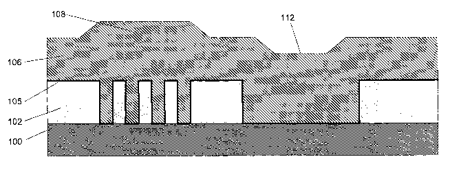
Figs. 1A and 1B illustrate an exemplary process flow of an
electropolishing method to polish a semiconductor structure that has a non-
planar
topology. Fig. 1A illustrates a dielectric layer 102 patterned with recessed
and
non-recessed areas formed over substrate 100. A barrier/seed layer 105 has
been
formed over the dielectric layer 102 and substrate 100. Finally, metal layer
106
has been deposited, for example, via electroplating over barner/seed layer 105
and covering the recessed and non-recessed areas of the dielectric layer 102.
Metal layer 106 has a non-planar topology that includes a hump 108 and a
recess
112 located over various structures in the dielectric layer. The non-planar
topology of metal layer 106 can be caused, for example, by the plating
chemistry
in an electroplating process.
With reference now to Fig. 1B, metal layer 106 is typically polished back
to the surface of the non-recessed areas such that metal layer 106 within the
recessed areas, i.e., the trenches, is isolated to form metal interconnection
lines.
In general, it is desirable to have the top surface of metal layer 106 within
the
recessed area planar with the top surface of the non-recessed area surrounding
metal layer 106 formed in the recessed area.
It should be recognized that references to planar are not intended to require
or suggest that the top surface of metal layer 106 be absolutely planar with
the top
surface of the non-recessed area; rather, it is intended to convey that the
level of
the top surface of metal layer 106 is made more even with the level of the top
surface of the recessed area. Thus, it is generally advantageous to reduce the
CA 02456225 2004-02-02
WO 03/017330 PCT/US02/26167
variation between the level of the top surface of metal layer 106 and the
level of
the top surface of the recessed area.
In this example, assume that metal layer 106 is electropolished.
Additionally, as depicted in Fig, 1A, assume that the profile or general shape
of
the topology of metal layer 106 is non-planar prior to electropolishing. As
noted
above, electropolishing is an isotropic etching process. As such, as depicted
in
Fig. 1B, the non-planar profile or general shape of the topology of metal
layer 106
can remain after electropolishing.
More particularly, in this example, as depicted in Fig. 1A, assume that the
topology of metal layer 106 includes hump 108 and concave portion 112 prior to
electropolishing. As depicted in Fig. 1B, assume that hump 108 and concave
portion 112 (Fig. 1A) remain as residue 110 and recess 114 after
electropolishing.
Residue 110 is a region of metal layer 106 at a height H above the dielectric
layer
102. Residue 110 can cause an electrical short circuit between interconnection
lines formed in the trench regions below residue 110. Recess 114 is a recess
or
trench in metal layer 106 where the surface of metal layer 106 within the
trench is
at a depth R below the surface of the dielectric layer 102. Recess 114 results
in
metal or copper loss within the trench that can cause a reduction of the
conductance of the formed interconnection lines. Thus, as noted above, it is
advantageous to reduce the variation in the height of the surface of metal
layer
106 above or below the surface of the non-recessed areas.
Accordingly, in one exemplary embodiment, a metal layer formed over a
patterned dielectric layer is planarized prior to electropolishing the metal
layer to
isolate interconnection lines. One advantage to planarizing the metal layer
prior
to electropolishing the metal layer back is that the metal interconnection
lines can
be formed in the dielectric layer with less damage to the structure underlying
the
metal layer than conventional planarizing techniques, and thus increase the
CA 02456225 2004-02-02
WO 03/017330 PCT/US02/26167
reliability of the interconnection elements since most damage to the structure
occurs when recessed metal is exposed to the CMP pad.
Figs. 2A through 2D illustrate an exemplary process flow of a method to
planarize and electropolish an exemplary semiconductor structure including a
metal layer 106 with a non-planar topology. Fig. 2A illustrates a cross-
section
view of an exemplary semiconductor structure with recessed areas 102r and non-
recessed areas 102n formed in a dielectric layer 102. The recessed areas 102r
and
non-recessed areas 102n form a pattern of interconnection lines in dielectric
layer
102. Dielectric layer 102 can be conventionally deposited and formed on
substrate layer 100 using any conventional deposition method, such as thermal
or
plasma chemical vapor deposition, spin-on, sputtering, or the like. Further,
dielectric layer 102 can be patterned through known patterning methods such as
photomasking, photolithography, microlithography, or the like. The dielectric
material may be, for example, silicon dioxide (Si02). For many applications it
is
desired to select a dielectric layer material having a low dielectric
constant, often
referred to as a low "k" value material. Low k value materials (i.e., less
than
approximately 3.0) provide better electrical isolation between interconnection
lines by reducing capacitance coupling and "cross-talk" between adjacent
lines.
Such low k value materials include flourinated silicate glass, polyimides,
fluorinated polyimides, hybrid/composites, siloxanes, organic polymers,
[alpha]-
C:F, Si-O-C, parylenes/fluorinated parylenes, polyterafluoroethylene,
nanoporous
silca, nanoporous organic, or the like.
Dielectric layer 102 is formed on substrate layer 100. Substrate layer 100
may be, for example, an underlying semiconductor wafer, previously formed
dielectric layers, or other semiconductor structures. Substrate layer 100 may
include, for example, silicon and/or other various semiconductor materials,
such
as gallium arsenide, or the like depending on the particular application.
CA 02456225 2004-02-02
WO 03/017330 PCT/US02/26167
A barner and/or seed layer 105 may also be deposited on the dielectric
layer by various methods, such as chemical vapor deposition (CVD), physical
vapor deposition (PVD), atomic layer deposition (ALD), or the like, such that
the
barner layer covers the patterned dielectric layer 102 including the walls of
dielectric layer 102 within the recessed areas 102r. A barrier layer serves to
prevent metal (e.g., copper) from diffusing into the dielectric layer 102
after the
subsequent metal layer 106 deposition (Fig. 2B). Any diffusion of copper into
the
dielectric layer 102 may adversely increase the dielectric constant of the
dielectric
layer 102. Barrier/seed layer 105 can be formed of a suitable conductive
material
that is resistant to the diffusion of copper, such as titanium, tantalum,
tungsten,
titanium-nitride, tantalum-nitride, tungsten-nitride, or other suitable
material. In
some applications, the barner layer can be omitted. For example, if the
dielectric
material is sufficiently resistant to the diffusion of the metal layer 106, or
if any
diffusion of metal layer 106 will not adversely affect the performance of the
semiconductor device, the barrier layer may be omitted.
A seed layer is typically deposited, for example, if metal layer 106 is
subsequently electroplated over dielectric layer 102. A seed layer is
typically a
thin layer of copper or other conductive material that metal layer 106 can be
electroplated onto. Further, a single layer or material of barner/seed layer 1
OS
may serve as both a barrier layer and a seed layer.
With reference now to Fig. 2B, metal layer 106 is deposited on the surface
of the barrier/seed layer 105, or on the dielectric layer 102 if the
barrier/seed layer
105 was omitted. Metal layer 106 fills the trenches or recessed areas 102r and
also covers the non-recessed areas 102n. Metal layer 106 may be deposited by
PVD, CVD, ALD, electroplating, electroless plating, or any other convenient
method. Metal layer 106 is, for example, copper or other suitable conductive
material such as aluminum, nickel, chromium, zinc, cadmium, silver, gold,
rhodium, palladium, platinum, tin, lead, iron, indium, or the like.
CA 02456225 2004-02-02
WO 03/017330 PCT/US02/26167
As shown in Fig. 2B, the topology of metal layer 106 may be non-planar
with variations in its topology. For example, the deposition of metal layer
106
can result in a hump 108 and/or concave portion 112 above various features of
dielectric layer 102. In particular, if metal layer 106 is electroplated over
the
dielectric layer 102, a hump 108 can form above a narrow and high-density
trench
region, and a concave portion 112 can form above a wide low-density trench
region of dielectric layer 102. The effects can be especially prevalent in the
case
of electroplating metal layer 106 over dielectric layer 102 because of the
plating
chemistry. It should be recognized, however, that the shape and location of
hump
108 and concave portion 112 are illustrative only and that other non-planar
topology features of metal layer 106 are possible as described below with
respect
to Figs. 4A and 4B.
With reference now to Fig. 2C, metal layer 106 is planarized to smooth or
reduce features of the topology. For example, a chemical mechanical polishing
(CMP) process is applied to the structure to polish and planarize metal layer
106.
CMP metal layer 106 reduces the topology, i.e., hump 108, recess 112, and
other
non-planar topology features of the surface of metal layer 106 to smooth metal
layer 106 prior to electropolishing metal layer 106. For example, the CMP
process is performed to polish metal layer 106 to a first height "a" above the
underlying substrate 100, where "a" is greater than a height "b," equal to the
height of dielectric layer 102. Therefore, the CMP process stops short of
removing metal layer 106 from the non-recessed areas 102n of dielectric layer
102
and possibly coming in contact with dielectric layer 102. Rather, the CMP
process polishes metal layer 106 to planarize and reduce variations in the
topology
of metal layer 106.
It should be recognized that references to planar and planarizing,
specifically in reference to metal layer 106, are not intended to require or
suggest
that the surface of metal layer 106 be absolutely planar; rather, it is
intended to
convey that the surface of metal layer 106 is made more smooth or planar.
CA 02456225 2004-02-02
WO 03/017330 PCT/US02/26167
Essentially, planarizing the surface of metal layer 106 reduces the variations
in the
topology of metal layer 106 prior to electropolishing.
The CMP process of this exemplary method can be optimized for
planarization efficiency, with less emphasis placed on preserving dielectric
layer
102 and the underlying structures because the polishing pad of the CMP
apparatus
(Fig. 5) does not directly contact the underlying structure, such as the
dielectric
layer 102. For example, the stiffness or hardness of a polishing pad may be
adjusted to preserve underlying dielectric layer 102. A stiff pad with a
diamond
tip embedded therein or the like can be used in the CMP portion of this
example
of the method. Further, slurry free or abrasive-free polishing processes can
be
used to reduce scratches in metal layer 106.
The pressure of the polishing pad can be a factor in controlling and
preventing damage to the patterned dielectric layer 102, and the interconnect
structure, particularly for integration schemes with copper and low k
dielectric
films. Typically the pressure of the polishing pad ranges from 0.1 pound-force
per square inch (PSI) to 10 PSI, for example 5 PSI. The thickness of metal
layer
106 removed during the CMP process depends, at least in part, on the
topography
of the metal layer 106 formed over dielectric layer 102 and the planarization
efficiency of the CMP process employed. Typically, the removal thickness is
greater than or equal to the difference between a high and low point of the
metal
layer topology.
It should be recognized, however, that the CMP process is described
herein for illustrative purposes only. Alternative methods of planarizing
metal
layer 106 may be used in place of, or with, the exemplary CMP process
described
above. For example, a sacrificial material may be added over metal layer 106
to
planarize the surface above metal layer 106. The sacrificial material can be
conductive or non-conductive such as spin-on-glass, photo-resist, metal alloy,
metal compound, or the like. The metal layer 106 may then be planarized, for
CA 02456225 2004-02-02
WO 03/017330 PCT/US02/26167
11
example, by etching away the sacrificial material and portions of metal layer
106.
The sacrificial material and metal layer 106 should have the same or similar
etch
rate such that an etching process removes the sacrificial layer and metal
layer 106
at similar rates. Etching the planarized metal layer 106 and the sacrificial
layer at
similar rates to remove the sacrificial layer and portions of metal layer 106
will
result in a planarized metal layer 106. An example of the process is depicted
in
Fig. 4A and described below.
The etching process can be a dry etching process or a wet etching process.
A dry etching process includes plasma etching, chemical vapor etching, and the
like. Plasma etching sources may include high-density plasma sources such as a
helicon plasma source, inductive coupled plasma source (ICP), and the like.
The
etching gas may include a halogen group such as chlorine based gases. Two
examples of the conditions for a plasma etching process are detailed in the
following tables:
Table I
EXEMPLARY PARAMETERS OF HIGH TEMPERATURE
PLASMA ETCHING PROCESS
Plasma power: 500 to 1500 W, preferably 800 W
Gas pressure: 10 to 50 mTorr, preferably 20 mTorr
Wafer temperature: 300 to 500 °C, preferably 400 °C
Etching gases: Chlorine (C12)
Table II
EXEMPLARY PARAMETERS OF LOW TEMPERATURE
PLASMA ETCHING PROCESS
Step 1:
Plasma power: 500 to 1500 W, preferably 800 W
Gas pressure: 10 to 50 mTorr, preferably 20 mTorr
Wafer temperature: 20 to 100 °C, preferably 50 °C
Etching gases: Chlorine (C12)
CA 02456225 2004-02-02
WO 03/017330 PCT/US02/26167
12
After Step 1 the top portion of copper and copper compound will
be converted to copper chloride (CuCIX).
Step 2:
Wet etch CuCIX compound by using dilute HCl solution. The
concentration of HCl may be in the range of 1 to 6 percent by weight,
preferably 3 percent.
Alternatively, a planarization technique similar to those used in the flat-
panel display industry to anneal the amorphous Si (a-Si) to poly-Si on glass
may
be employed to reflow copper after plating metal layer 106 by using a laser to
mollify metal layer 106 resulting in a planarized surface. Another alternative
method includes a high frequency and short pulse laser that can be beamed from
a
direction parallel to the substrate 100 surface to remove higher portions of
the
topology of metal layer 106 by evaporation. The short pulse of the laser is
used to
protect bulk copper and surrounding dielectrics from the effects of high
temperatures generated by the laser, i.e., reduce thermobudget. The laser can
be a
solid state laser such as a ruby laser, Nd-glass laser, Nd:YAG (yttrium
aluminum
garnet, Y3AlsOla) laser, gas laser, such as a He-Ne laser, COa laser, HF
laser, or
the like. The laser beam can be scanned over the entire surface of substrate
100 to
planarize metal layer 106. Further, a non-contact type surface topography
sensor
can be used as an end-point detector in such a process. Exemplary conditions
for
this planarization process are detailed in the following table:
Table III
EXEMPLARY PARAMETERS OF PULSED LASER
PLANARIZATION PROCESS
Average laser power: 100 to 5000 W
Pulse length: Picoseconds to microseconds
Wafer temperature: - 100 to 20 °C
CA 02456225 2004-02-02
WO 03/017330 PCT/US02/26167
13
With reference now to Fig. 2D, after metal layer 106 has been planarized,
metal layer 106 is electropolished. Specifically, metal layer 106 is
electropolished
from the non-recessed areas 102n of dielectric layer 102 such that metal layer
106
is isolated within recessed areas 102r, or trenches, to form interconnection
lines.
Metal layer 106 can be polished to the same height as the non-recessed areas.
Alternatively, metal layer 106 can be polished to a height below the non-
recessed
areas. Metal layer 106 can be electropolished by an electropolishing apparatus
(Fig. 6) that directs a stream of electrolyte fluid (not shown) to metal layer
106.
The electrolyte fluid is, for example, any convenient electropolishing fluid,
such
as phosphoric acid, orthophosphoric acid (H3P04), or the like.
Further, barrier/seed layer 105 is removed from the exposed regions of
non-recessed areas 102n of dielectric layer 102. If layer 105 is, or includes,
a seed
layer, the electropolishing process that polishes metal layer 106 may remove
it,
for example. If layer 105 is, or includes, a barrier layer, plasma dry
etching, wet
etching, or the like may remove it, for example. Additionally, if the metal
layer
106 was electropolished to a height less than the non-recessed areas, the non-
recessed areas can also be etched at this time to planarize the surface. The
following table; Table IV, provides an exemplary range of parameters that can
be
employed in a plasma dry etch process to remove the barrier layer:
Table IV
EXEMPLARY PARAMETERS OF PLASMA DRY ETCH
PROCESS
Plasma Power: 500 to 2000 W
Vacuum: 30 to 100 mTorr
Temperature of Wafer: approximately 20° C
Gas and flow rate: SF6 = 50 sccm (or CF4 = 50
sccm, or Oz =10 scan)
Gas pressure: 0.1 to 50 mTorr
Removal rate of TaN: 250 nm/min
CA 02456225 2004-02-02
WO 03/017330 PCT/US02/26167
14
Removal rate of TiN: 300 nm/min
Removal rate of Si02: 20 nm/min
These parameters result in a removal rate of TaN and TiN, two possible
barrier layer 105 materials, greater than that of Si02, a possible dielectric
layer
102 material. The selectivity can be selected in this manner to reduce etching
or
damaging the underlying dielectric layer 102 during the removal of the barrier
layer 105. It should be noted, however, that other selectivities can be
obtained by
varying the parameters.
Fig. 3 is a flow chart illustrating an exemplary damascene process 300
including a planarizing process and an electroplating process. A wafer having
recessed and non-recessed areas is provided in block 302. A patterned
dielectric
layer provided on the wafer may define the recessed and non-recessed areas.
The
patterned dielectric layer may be formed on underlying semiconductor
structures,
including other previously formed dielectric layers, a wafer, or the like.
Further,
the wafer may be divided up into individual dice that include recessed and non-
recessed areas that will be separated at a later state of the processing into
individual semiconductor devices. A metal layer is then deposited in block
304,
such that the metal layer fills the recessed areas within the dielectric layer
as well
as covers the non-recessed areas of the dielectric layer. The metal layer is
then
planarized in block 306. For example, the metal layer undergoes a CMP process
to planarize and smooth the topography of the metal layer. The planarized
metal
layer is then electropolished in block 308 to expose the non-recessed areas of
the
dielectric layer and isolate the metal layer within the recessed areas to form
metal
interconnection lines.
It should be recognized that numerous modifications can be made to the
exemplary process 300 depicted in the flow chart. For example, a barrier/seed
layer can be optionally added prior to the deposition of the metal layer in
block
304, in which case, after non-recessed areas are exposed, the barrier/seed
layer is
CA 02456225 2004-02-02
WO 03/017330 PCT/US02/26167
etched from the dielectric layer. Additionally, each block in Fig. 3 can
include
many processes not explicitly described herein, such as masking and etching
the
wafer to form the recessed areas, or cleansing the metal layer before and/or
after
planarizing the surface. Further, the exemplary damascene process 300 is
applicable to both single and dual inlaid applications.
Figs. 4A and 4B illustrate additional exemplary topologies of metal layer
106 that may be planarized and then electropolished to form interconnection
structures. With regard to Fig. 4A, metal layer 106 has a topology that
roughly
corresponds to the shape of the underlying dielectric layer 102. Such a
topology
could be created, for example, by sputtering metal layer 106 over dielectric
layer
102. Metal layer 106 is then planarized, for example, by adding a sacrificial
material 107 and then etching back the sacrificial material 107 and a portion
of
metal layer 106 such that metal layer 106 is plana~ized to dotted line "P." As
described above, sacrificial material 107 can be a metal, metal composites
with
solvent, such as copper with a solvent, spin-on glass, photo-resist, or the
like.
Sacrificial material 107 can be any material that has a similar etching rate
as the
underlying metal layer 106, and the etching process can be a conventional dry
or
wet etch with no selectivity between sacrificial material 107 and metal layer
106.
The location of line "P" is for illustrative purposes only, and can be
adjusted up or down depending on the application and method of planarization.
After the topology features of metal layer 106 have been planarized, similar
to
Fig. 2C, metal layer 106 is then electropolished as described above with
regard to
Fig. 2D.
Fig. 4B illustrates another exemplary metal layer 106 having an irregular
surface topology. The irregular surface topology of metal layer 106 may be due
to any number of causes ranging from the deposition method to the underlying
structure. Metal layer 106 is polished similar to Fig. 4A by first planarizing
the
surface to line "P," by CMP polishing, adding a sacrificial material and
etching
CA 02456225 2004-02-02
WO 03/017330 PCT/US02/26167
16
back, momentarily heating metal layer 106 with a laser or the like. Metal
layer
106 is then electropolished. It should be recognized from Figs. 4A and 4B that
numerous metal layer topologies can be planarized and electropolished by this
method without undue damage to the underlying dielectric layer 102.
With reference now to Fig. 5, an exemplary CMP apparatus 400 and
process are described. CMP apparatus 400 may be used to planarize metal layer
106. An exemplary CMP process proceeds by pressing and rotating the surface of
a wafer against a wetted polishing surface. The process is controlled through
the
chemical, pressure, and temperature conditions of CMP apparatus 400.
Exemplary CMP apparatus 400 includes a rotatable polishing platen 411 and a
polishing pad 412 mounted on polishing platen 411. CMP apparatus 400 also
includes a rotatable wafer carrier 413 that positions and applies a force to a
wafer
401 in the direction indicated by arrow 414. A chemical slurry is supplied to
CMP apparatus 400 through nozzle 417 and dispensed onto the polishing pad 412.
The chemical slurry is, for example, supplied from a temperature-controlled
reservoir (not shown) through nozzle 417. Further, the chemical slurry
contains a
polishing agent, such as alumina, silica, or the like that is used as an
abrasive
agent along with other selected chemicals to polish the surface of wafer 401.
The primary parameters that affect the polishing rate are the down
pressure 414 on the wafer 401 against polishing pad 412, the rotational speeds
of
the polishing platen 411 and wafer Garner 413, the composition and temperature
of the chemical slurry, and the composition of polishing pad 412. Adjushnents
of
these parameters permit control of the polishing rate and the planarization
efficiency of CMP apparatus 400.
CMP apparatus 400 and the process described with reference to Fig. 5, are
for illustrative purposes only. It should be recognized that other CMP
apparatus
configurations and set-ups may be employed. For example, rotatable polishing
platen 41 l and polishing pad 412 can be replaced with a belt that moves
polishing
CA 02456225 2004-02-02
WO 03/017330 PCT/US02/26167
17
pad 412 with respect to wafer carrier 413. Also, as will be recognized, the
movement of wafer 401 with respect to polishing pad 412 can be achieved in
numerous manners. Therefore, the CMP apparatus 400 depicted in Fig. 5 is not
intended to be limiting of the CMP apparatus or method that may be used.
Fig. 6 illustrates an exemplary cross-sectional view of an electropolishing
apparatus 500 that can be used to electropolish metal layer 506 formed on
semiconductor wafer 501. Semiconductor wafer 501 may further include, for
example, substrate layer 100, dielectric layer 102, and barrier/seed layer 105
(Figs
2A through 2D). Further, the topology of metal layer 506 will have been
planarized prior to the electropolishing, for example, by CMP apparatus 400
(Fig.
5).
A nozzle 540 of the electropolishing apparatus 500 directs a stream of
electrolyte fluid 520 to the surface of metal layer 506. In other examples,
wafer
501 can be completely or partially immersed in electrolyte fluid 502.
Electrolyte
fluid 520 includes any convenient electropolishing fluid, such as phosphoric
acid,
orthophosphoric acid (H3P04), or the like. For example, in one example the
electrolyte fluid is orthophosphoric acid having a concentration between about
60
percent by weight and about 85 percent by weight. Additionally, electrolyte
fluid
106 can include, for example, glycol at 10 to 40 percent (against weight of
the
acid). It should be recognized, however, that the concentration and
composition
of the electrolyte fluid can vary depending on the particular application.
As electropolishing apparatus 500 directs a stream of electrolyte fluid 520
to metal layer 506, a power supply 550 supplies opposing charges to an
electrode
530 (the cathode) positioned in nozzle 540 and an electrode (the anode)
coupled
to metal layer 506. Power supply 550 can, for example, operate at a constant
current or constant voltage mode. With power supply 550 configured to
positively charge the electrolyte fluid 520 relative to metal layer 506, metal
ions
of metal layer 506 are removed from the surface. In this manner the stream of
CA 02456225 2004-02-02
WO 03/017330 PCT/US02/26167
18
electrolyte fluid 520 electropolishes the portion of metal layer 506 in
contact with
the stream of electrolyte fluid 520.
Further, as depicted in Fig. 6, wafer 501 is rotated and translated along
axis X to position the entire surface of metal layer 506 in the stream of
electrolyte
fluid 520 and uniformly electropolish the surface. For example, the
electrolyte
fluid 520 can make a spiral path along the surface of metal layer 506 by
rotating
wafer 501 while simultaneously translating wafer 501 in the X direction.
Alternatively, wafer 501 can be held stationary while nozzle 540 is moved to
apply the stream of electrolyte 520 to desired portions of metal layer 506.
Further, both wafer 501 and nozzle 540 can move to apply the stream of
electrolyte 520 to desired portions of metal layer 506. Exemplary descriptions
of
electropolishing methods and apparatus may be found in U.S. Patent Application
No. 09/497,894, entitled METHODS AND APPARATUS FOR
ELECTROPOLISHING METAL INTERCONNECTIONS ON
SEMICONDUCTOR DEVICES, filed on February 4, 2000, and related U.S.
Patent No. 6,395,152, entitled METHODS AND APPARATUS FOR
ELECTROPOLISHING METAL INTERCONNECTIONS ON
SEMICONDUCTOR DEVICES, filed on July, 2, 1999, both of which are
incorporated herein by reference in their entirety.
Additionally, it should be recognized that other electropolishing methods
and apparatus can be employed to electropolish metal layer 106. For example,
wafer 501, including metal layer 506, may be partially or fully immersed
within a
bath of electrolyte fluid.
The above detailed description is provided to illustrate exemplary
embodiments and is not intended to be limiting. It will be apparent to those
skilled in the art that numerous modification and variations within the scope
of the
present invention are possible. For example, numerous interconnect structures,
such as combinations of dielectric layers, conductive layers, barner layers,
seed
CA 02456225 2004-02-02
WO 03/017330 PCT/US02/26167
19
layers, and mask layers, formed in single or dual inlaid damascene
implementations, can be planarized and electropolished with the methods
described. Further, numerous methods of planarizing and electropolishing can
be
combined to planarize and electropolish the surface of the interconnection
structures. It should also be apparent to those skilled in the art that metal
layers
with non-planar topologies, created for reasons other than those described
herein,
can be advantageously planarized and electropolished in accordance with the
methods and apparatus described. Accordingly, the present invention is defined
by the appended claims and should not be limited by the description herein.