Note : Les descriptions sont présentées dans la langue officielle dans laquelle elles ont été soumises.
403027-A-11-CA (Norte)
CA 02457252 2004-02-09
Ultra-High-Frequency Notch Filter
Technical Field
This invention relates to suppression of electromagnetic
interference (EMI).
Background of the Invention
Use of high-bandwidth transmission lines to implement local
area networks (LANs) is becoming increasingly common. An example
thereof is the Gigabit Ethernet LAN. The high-frequency transmission
affected by such transmission lines make suppression of their radiated
1o emissions a significant challenge, on account of the fact that radiated
emissions, and the crosstalk to other signal lines caused thereby,
increase as transmission frequency increases.
A notch filter is designed to reject a band of frequencies while
passing through all other frequencies. Although the use of notch filters
to filter out EMI is known (see, e.g., U.S. patent no. 6,539,253), a
technical challenge in developing a notch filter for EMI suppression is
how to effectively deal with parasitic inductance and capacitance,
which can deleteriously affect the intended performance of the filter. At
ultra-high transmission frequencies, even small parasitic effects can
2o cause significant problems and therefore must be accounted for in the
notch filter design.
Summary of the Invention
This invention is directed to solving these and other problems
and disadvantages of the prior art. According to one aspect of the
invention, an apparatus comprises a capacitor having a body and a
pair of terminals attached to the body, and a conductor defined on the
body and connecting the terminals, the conductor having an inductance
defining together with a capacitance of the capacitor a parallel LC
circuit. The circuit is tuned by varying the width of the traces. The
3o apparatus is illustratively suited for use as a notch filter. According to
another aspect of the invention, a notch filter having a notch center
frequency comprises a capacitor that has a body and a pair of
1 of 12
403027-A-11-CA (Norte)
CA 02457252 2004-02-09
terminals attached to the body and that has a resonant frequency equal
to or greater than the notch center frequency, and further comprises a
conductive trace that has an inductance and that extends along the
body and connects the terminals. Illustratively, when mounted on a
printed circuit board (PCB) in a signal line proximate to a ground plane,
the notch filter and the ground plane form a virtual conductive loop the
product of whose inductance and capacitance is the notch center
frequency. According to yet another aspect of the invention, a PCB
comprises a signal conductor comprising a pair of discrete conductor
~o segments defined by the PCB, a ground plane defined by the PCB, a
capacitor having a body and a pair of terminals on the body that
connect the capacitor between the segments, and a conductor defined
on the body and connecting the pair of terminals. The conductor has
an inductance and forms with the capacitor a notch filter for the signal
conductor such that the product of the inductance and the capacitance
of a virtual conductive loop formed by the notch filter and the ground
plane equals a center frequency of the notch of the notch filter.
Advantages of the invention include a notch filter that is effective
at ultra-high frequencies, that is easy to construct, that is tuneable, that
2o minimizes the number of parts used in its construction, that is compact
so that it takes up little real estate on a printed circuit board, and that is
compatible with surface-mount circuit-assembly techniques.
Brief Description of the Drawing
These and other features and advantages of the invention will
25 become more apparent from the following description of an illustrative
embodiment of the invention considered together with the drawing in
which:
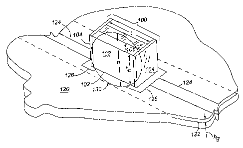
Fig. 1 is a perspective diagram of a printed-circuit-board-
mounted notch filter that includes an illustrative embodiment of the
3o invention;
Fig. 2 is a graph of load lines of capacitors illustratively used to
implement a 1 GHz notch filter;
2of12
403027-A-11-CA (Norte)
CA 02457252 2004-02-09
Fig. 3 is a graph of load lines of capacitors illustratively used to
implement a 4.8 GHz notch filter; and
Fig. 4 is a graph of load lines of capacitors illustratively used to
implement a 6.25 GHz notch filter.
s Detailed Description
Fig. 1 shows an illustrative embodiment of a notch filter 100
mounted on a printed-circuit board (PCB) 120. Notch filter 100 spans
two segments 124a and 124b of a printed-circuit conductor 124
carrying signals that are to be filtered for EMI. Each segment of
~o conductor 124 terminates in a solder pad 126 to which notch filter 100
is electrically connected, e.g., by a component surface-mounting
process.
Notch filter 100 consists of a capacitor 102, preferably a surface-
mount capacitor, and a conductive trace 106 of width w and length I
15 defined by (e.g., plated or printed on) and extending the length of body
103 of capacitor 102. Capacitor 102 is electrically connected to solder
pads 126 by conductive terminals 104 that extend from opposite ends
of body 103 of capacitor 102. Trace 106 is electrically connected to
terminals 104, and acts as an inductor there between. Capacitor 102
2o and trace 106 together form a parallel inductive-capacitive (LC) circuit
between the segments of conductor 124. PCB 120 has a ground plane
122 as one of its layers, which serves as a return path for signals
conducted by conductor 124. Ground plane 122, capacitor 102, and
trace 106 together form a virtual conductive loop 130 at the resonant
25 frequency of the structure that is formed by them. Loop 130 has a
height h, which is the distance between trace 106 and ground plane
122. hi consists of the height h~ of capacitor 102 and depth hg at which
ground plane 122 is buried in PCB 120. A standard thickness of PCB
120 is 62 mils; consequently, h9 is normally anywhere between 1 mil
3o and 61 mils. The product of the capacitance (C) and inductance (L) of
loop 130 define the center frequency f~ of the notch implemented by
filter 100 that will be filtered out of the signals on conductor 124.
3 of 12
4'03027-A-11-CA (Norte)
CA 02457252 2004-02-09
As is known, capacitors have an individual resonant frequency f~
below which they behave capacitively and above which they behave
inductively. Typically, the smaller is the capacitance of a capacitor, the
smaller is its physical package, and the higher is its resonant frequency
f~. For ease of design, it is desirable that f~ of capacitor 102 equal or
exceed f~. At this f~, the capacitance C of loop 130 is effectively the
capacitance of capacitor 102. Consequently, the required inductance L
of loop 130 is L = 1/(4~2fC). Inductance L is provided by loop 130.
Inductance L is related to loop height h, as follows: L = 5(10'3) In (~h' )
d
io I, where L is measured in NH, h, is measured in mils, I is the length of
trace 106 in inches, and d is the diameter in mils of an equivalent
circular cross-section having a circumference ~d equal to twice the
sum of the width w and thickness t of trace 106. L is tuned by varying
the width w of trace 106. It is assumed that the thickness t of trace 106
is is a standard and unvarying approximately 1 mil (.-.7 to ~1.4 mil) of
copper, aluminum, or other conductor; i.e., the standard thickness of a
printed circuit trace. Given the dimensions of conventional surface-
mountable capacitors, values of L that are reasonably achievable by
varying the width w of trace 106 are between about .2 nH and about
20 1.5 nH.
In this illustrative example, it is assumed that conductor 124
suffers from EMI or crosstalk from a Gigabit Ethernet, i.e., f~=1 GHz.
Given f~ and the reasonably-achievable values of L, an available
suitable capacitor 102 is selected. In this example, an illustrative
25 commercially-available capacitor is a surface-mountable 0603-type
capacitor (length of 60 mils, width and height of 30 mils) of 27 pF. The
selection of capacitor 102 determines height h, of loop 130 (h9 being
fixed by PCB 120) and length I of trace 106. The inductance L of loop
130 therefore must be tuned to produce the desired value of f~ by
so varying the width w of trace 106.
The proper width w of trace 106 is determined from the following
formulas.
4of12
CA 02457252 2004-02-09
403027-A-11-CA (Nome)
2(h, + h.K )Tc
L(hx , w, t, l) = 5.0(10-6 ) ~ l ~ In , where
(w+r)
L = inductance (in pH) of loop 130
h9 = vemical distance from bottom surface of capacitor 102 to the
return reference plane 122 (in mils)
h, = height of capacitor 102 (in mils)
w = width of trace 106 (in mils)
t = thickness (height) of trace 106 (in mils)
I = length of trace 106 (in mils)
f"(h~,w,t,l,C)= ~ , where
2~ L(hg,y,t,l)~C
f" = center frequency of the notch filter, and
C = capacitance (in farads) of loop 130
The procedure for determining w, and h9 for fixed t, I, and C
i5 values is as follows:
(1) Plot f"(hg,w,t,I,C) for 1<h9<hP~b (total thickness of PCB 120 in mils)
and Sl <_ w <_ h, in mils as a surface plot, with h9 as the x-axis and
w as the y-axis. The vertical z-axis is then the resonant frequency
2o for a given (h9, w) pair.
(2) Superimpose a "reference" surface plot on top of the surface plot
generated from step (i) that represents the desired resonant
frequency f". This surface plot will necessarily be a planar surface
and should cover the entire (hg, w) range of values as stated in step
25 (1).
(3) The intersection of the surface plot from (t) and the planar surface
plot from (2) represents the full range of (h9, w) pairs that will
produce the desired resonant frequency. This intersecting contour
will be a line, referred to as a load line. Implement the solution by
3o fabricating an electroplated copper trace t06 of length I (mils), and
width w (mils).
5 of 12
403027-A-11-CA (Norte)
CA 02457252 2004-02-09
(4) If no intersection results from step (3), alter the value of the
capacitance C until an intersecting contour is generated from the
two surface plots. Make sure to select C such that This capacitor
behaves capacitively slightly beyond the desired resonant
frequency. In other words, the selected capacitor must have a
resonant frequency f~ that exceeds the desired resonant frequency
f" of the notch filter.
(5) If the variable h9 is known a-priori, then select the (h9, w) pair that
lies on the load line determined from step (3). Implement the
~ o solution by fabricating trace 106 of length I, and width w. Usually
h9 is known a-priori, since the layer stackup of printed circuit board
120 is known before designing the notch filter.
Fig. 2 shows a load line 204 that defines the value of w as a
15 function of h9 at f~=1 GHz for a 27 pF 0603-type capacitor. As
described above load line 204 is derived by superimposing two surface
plots, with their intersection being the load line for a given notch filter
center frequency fn.One of the surface plots is a plot of the achievable
resonant frequencies as a function of the width w of trace 106 and the
2o depth h9 of the reference return path. This surface plot is for a given
fixed capacitance of 27 pF in this example. Also, in this example, h, _
(30 + h9) mils. Next, a reference plane is superimposed onto the
aforementioned first surface plot. This reference plane is the desired
notch filter resonant frequency f" of 1 GHz in this example. The
25 intersection of these two surfaces is line 204 that highlights the needed
width of trace 106 as a function of the depth h9 of ground plane 122
within printed circuit board 120. The 27 pF 0603-type capacitor is
currently believed to be the only capacitor that will provide a 1 GHz
notch filter for any depth of ground plane 122 within a conventional 62
3o mil thick printed circuit board 120. There are other capacitor values
that can provide a 1 GHz notch filter; however, these other values will
prevent the depth h9 of ground plane 122 from covering the entire 62
mil thickness of PCB 120. In these cases, the depth hg of ground plane
122 must be greater than some minimal depth, or will only work within
6of12
403027-A-11-CA (Norte)
CA 02457252 2004-02-09
some subset of the entire 62 mil PCB thickenss. These constraints are
restrictive and limit the practicality of using anything but an 0603-type
27 pF capacitor.
Computer simulations indicate that notch filter 100 constructed
as described above produces an attenuation better than 7 dB of the 1
GHz EMI.
Instead of using one capacitor 102 and trace 106 to implement
notch filter 100, a plurality of capacitors can be connected in parallel to
form capacitor 102, and one or more of those capacitors can carry
1o traces that together, in parallel, form trace 106. If capacitors of
slightly-
different values are used in parallel, the result is a plurality of slightly-
different notch filters - or, equivalently, a notch filter having a wider
notch - resuting in improved EMI attenuation. One of the advantages
of a notch filter 100 constructed in the illustrative manner is that it
i5 occupies a very small amount of PCB real estate. To preserve this
advantage in the case of a notch filter costructed from a plurality of
capacitors, the capacitors may be vertically stacked, illustratively as
described in U.S. patent aplication serial no. 10/292,670, filed on
November 12, 2002, and assigned to the same assignee as this
2o application. In this illustrative example of a 1 GHz notch filter, a 23 pF
0603-type capacitor may be used in parallel with the 27 pF capacitor.
The load line for the parallel combination of the 23 pF and 27 pF
capacitors is shown as load line 202 in Fig. 2.
Of course, the invention may be used to implement notch filters
25 at frequencies other than 1 GHz. Illustatively, Fig. 3 shows a load line
304 for a surface-mountable 0402-type capacitor (length of 40 mils,
width and height of 20 mils) of 1.7 pF used to implement a 4.8 GHz
notch filter. Correspondingly to the example Fig. 2, the 1.7 pF
capacitor may advantageously be used in parallel with a 0402-type
so capacitor of 1.508 pF to implement the 4.8 GHz notch filter. The load
line for the parallel combination of the two capacitors is shown as toad
line 302 in Fig. 3. Also illustratively, Fig. 4 shows load line 404 for a
surface-mountable 0402-type capacitor of 1.023 pF used to implement
a 6.1 GHz notch filter. Again, this capacitor may advantageously be
7 of 12
4'03027-A-11-CA (Norte)
CA 02457252 2004-02-09
used in parallel with an 0402-type capacitor of 0.9 pF to implement the
6.1 GHz notch filter. The load line for the parallel combination of the
two capacitors is shown as load line 402 in Fig. 4.
Of course, various changes and modifications to the illustrative
embodiment described above will be apparent to those skilled in the
art. These changes and modifications can be made without departing
from the spirit and the scope of the invention and without diminishing
its attendant advantages. It is therefore intended that such changes
and modifications be covered by the following claims except insofar as
limited by the prior art.
8 of 12