Note : Les descriptions sont présentées dans la langue officielle dans laquelle elles ont été soumises.
CA 02458438 2004-02-18
ELECTRONIC PACKAGE WITH STRENGTHENED CONDUCTIVE PAD
The present invention relates, in general, to electronics packages, one
example being a
chip carrier having a circuitized substrate for interconnecting a
semiconductor chip to a printed
circuit board. In particular, the invention relates to such circuitized
substrates packages and the
like for use in information handling systems (e.g., computers).
Circuitized substrates, such as those used in electronic packages, have been
and continue
1o to be developed for many applications. Such a circuitized substrate usually
includes a surface for
redistributing electrical signals from the chip mounted on the circuitized
substrate onto a larger
circuitized area so that the circuitized substrate can properly interface with
the hosting printed
circuit board having said larger area.
15 With semiconductor chip input/output (I/O) counts increasing beyond the
capability of
peripheral lead devices and as the need for both semiconductor chip and
printed circuit board
miniaturization increases, area array interconnects will be the preferred
method for making a
large number of connections between an electronic package such as a chip
Garner and a printed
circuit board. For circuitized organic substrates, including chip Garners and
printed circuit
2o boards, it is known that the materials making up these substrates have some
structural flexibility.
All flexible materials have some limitations on the amount of mechanical
strain which can be
tolerated until the material fractures and fails. A measure of this is
commonly known as
ductility. During manufacture of an electronic package and its assembly to a
printed circuit
board, many sources of package substrate (laminate) and printed circuit board
flexure or bending
25 exist. Sources include manual handling through assembly, placing the
printed circuit board into
tooling fixtures, assembling other components onto the printed circuit board,
assembly of cables
and hardware to the printed circuit board and use of pressure-probes for
electrical testing.
Furthermore, if the coefficient of thermal expansion (CTE) of the
semiconductor chip, the
package's laminate substrate, and the printed circuit board are substantially
different from one
3o another, temperature changes during operation of the electronic package can
cause flexure or
bending of the organic structures by different amounts. As a result, industry
standard ball grid
CA 02458438 2004-02-18
array (BGA) interconnections between the package and printed circuit board may
be subject to
high stress. These high stresses can be transmitted into the package and can
potentially cause
high strain on the package's materials beyond the limits of the material
ductility, and cause
package damage. Significant yield loss concerns during manufacturing, and
reliability concerns
during thermal cycling field operation may become manifest by failure
(cracking or
delamination) of dielectrics and circuitry on or within the chip carrier or
even failure of the
integrity of the semiconductor chip (chip cracking) caused by high stress
during manufacturing
and field operation. These concerns significantly inhibit design flexibility.
For example,
semiconductor chip sizes may be limited or interconnect sizes, shapes and
spacing may have to
1o be customized outside or beyond industry standards to reduce these
stresses. These limitations
may limit the electrical performance advantages of the electronic package
and/or add significant
cost to the electronic package.
One particular yield and reliability concern is that of the circuitized
substrate's external
~ 5 conductive layer, which is used to electrically bond the package to the
printed circuit board, with
the aforementioned solder ball grid array. This layer may be susceptible to
stresses transmitted
from the printed circuit through the BGA solder ball interconnections from
handling or thermal
cycling of the electronic package. If the layer (and an accompanying solder
mask layer if
utilized) cannot accommodate the stresses, then it is susceptible to
deterioration, such as cracking
20 or partial separation, which can cause failure of the formed connection
(and the electronic
package). Even worse, such failure may also cause failure of the information
handling system
utilizing the package. By the term information handling system as used herein
is meant an
instrumentality or aggregate of instrumentalities primarily designed to
computer, classify,
process, transmit, receive, retrieve, originate, switch, store, display,
manifest, measure, detect,
25 record, reproduce, handling or utilize any form of information,
intelligence or data for business,
scientific, control or other purposes. Examples include personal computers and
larger
processors such as servers, mainframes, etc.
High stresses transmitted to the upper layers) of such a package substrate
will typically
30 occur at the edges of the BGA interconnection pads and will be highest at
the edges of the BGA
interconnection pads under the rows of BGA solder ball interconnections at or
near a corner of
CA 02458438 2004-02-18
the package's usually rectangular substrate. To a lesser extent, high stresses
transmitted to this
layer can also occur at the edges of the BGA interconnection pads under the
rows of BGA solder
ball interconnections at or near the non corner edges of the chip Garner.
Cracks in or separation
of the conductive layer caused by the flexure, described above, generally
initiate in these areas of
highest stress. Solutions to this problem which limit or reduce the amount of
printed circuit
board flexure can be impractical and overly restrictive.
Thus, it is desirable to have an electronic package with a laminate,
circuitized substrate
that substantially inhibits or prevents separation and/or cracking of the
external circuit pattern
1o during flexure of the package caused by assembly, handling or operation.
The package (and
system) defined herein will have improved yield and increased field life
operation, and thus
represent an advancement in the art.
Accordingly, it is the object of this invention to enhance the art of
electronic packaging
15 and of information handling systems utilizing same.
It is another object of the invention to provide an electronic package that
includes a
circuitized substrate that can be manufactured in such a manner that
substantially inhibits or
prevents cracking or separation of a circuit pattern (e.g., pad) positioned on
the surface of the
2o package's circuitized substrate, has increased yields, and can be produced
at relatively
competitive costs compared to many current products.
It is still another object of the invention to provide an information handling
system
utilizing such an electronic package mounted on a suitable substrate such as a
printed circuit
25 board which in turn is positioned in the system.
According to one aspect of the invention, there is provided an electronic
package
comprising a substrate having an external surface, an electrically conductive
pad positioned on
the external surface, and at least one electrically conductive layer
positioned within the substrate
and physically coupled to the electrically conductive pad, the at least one
electrically conductive
30 layer of a size sufficiently large enough to substantially prevent removal
of the electrically
CA 02458438 2004-02-18
conductive pad when the pad is subjected to a tensile pressure of at least
about 1.4 grams per
square mil.
According to another aspect of the invention, there is provided an information
handling system comprising at least one printed circuit board including at
least one
electrically conductive receptor thereon, an electronic package including a
substrate having an
external surface, an electrically conductive pad positioned on the external
surface, and at least
one electrically conductive layer positioned within the substrate and
physically coupled to the
electrically conductive pad. The at least one electrically conductive layer is
of a size
to sufficiently large enough to substantially prevent removal of the
electrically conductive pad
when the pad is subjected to a tensile pressure of at least about 1.4 grams
per square mil. The
system further includes an electrically conductive member secured to the
electrically
conductive pad and electrically coupled to the at least one electrically
conductive receptor to
connect the electronic package to the at least one printed circuit board.
The above objects, advantages and features ofthe present invention will become
more
readily appaxent from the following detailed description of the presently
preferred
embodiments as illustrated in the accompanying drawings.
2o FIGS. 1 and lA represent partial top and side elevational views of an
electronic
package substrate, respectively, showing the substrate's conductive pad
coupled to an
underlying conductive layer;
FIGS. 2 and 2A illustrate partial top and side elevational views of an
electronic
package substrate, respectively, according to one embodiment of the invention;
FIGS. 3 and 3A illustrate, respectively, partial top and side elevational
views of
another embodiment of a substrate for use with the invention;
CA 02458438 2004-02-18
FIGS. 4 and 4A illustrate partial top and side elevational views,
respectively, of still
another embodiment of a substrate for use with the invention;
FIGS. 5-8 illustrate various embodiments of electrically conductive pins
usable in the
present invention;
FIG. 9 illustrates a side elevational view of an electronic package according
to one
embodiment of the invention, the package being electrically coupled to a hose
substrate such as a
printed circuit board;
FIG. 10 is a side elevational view, on a reduced scale over that of FIG. 9,
showing an
electronic package and circuit board assembly, further including additional
components (i.e.,
heat sink); and
FIG. 11 is a perspective view of an information handling system according to
one
embodiment of the invention, the system including a package-board subassembly
of the type
depicted in FIG. 10.
For a better understanding of the present invention, together with other and
further
objects, advantages and capabilities thereof, reference is made to the
following disclosure and
appended claims in connection with the above-described drawings. It is
understood that like
numerals will be used to indicate like elements from FIG. to FIG.
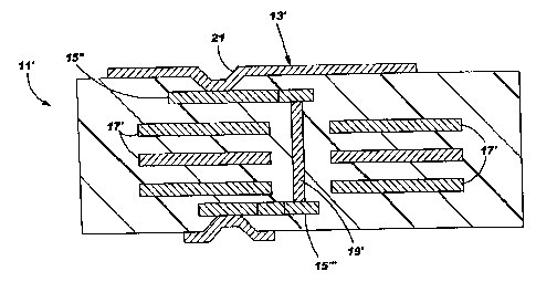
In FIGS. 1 and lA, there is shown the circuitized substrate 11 of the
electronic package
described in parent application S.N. 10/392,617, filed 03/20/03 under attorney
docket number
END920020058US1. FIG. 1 is a partial overhead plan view showing the
electrically conductive
pad 13 but not the underlying substrate on which this pad is positioned. Pad
13 is physically
coupled to an internal conductive layer 15 as shown, which internal conductive
layer may also be
connected to additional conductive layers 17 and/or a vertically oriented
conductive via (or
3o through) hole 19 to be connected to these other conductive layers. In the
example in FIG. lA,
layer 15 is connected using the conductive via 19 to a similar layer 15'
located on the opposite
5
CA 02458438 2004-02-18
surface of substrate 11. It is also possible for layer 15 to be connected to
selected ones of layers
17 using the conductive via 19 by merely extending the respective conductive
layers to
physically connect to via 19. As seen in the overhead view of FIG. 1,
conductive pad 13 of S.N.
10/392.617 includes an indented via portion 21 in addition to a substantially
planar portion 23
located on the substrate's upper surface. The indented via portion extends
through at least one
layer of dielectric material which forms part of the multilayered substrate 11
to form the
physical connection with underlying conductive layer 15. As specifically see
in FIG. 1, the
underlying conductive layer 15 (shown hidden in FIG. 1) includes an annular
portion 25 of
substantially the same outer diameter as indented via 21, a relatively narrow
connection portion
27 and a second annular portion 29 which forms the electrical connection to
the via 19. This
structure for underlying layer 15 is referred to as a "dog-bone"
configuration, as also explained in
S.N. 10/392,617.
It is understood that substrate 11 comprises a plurality of conductive layers
as shown in a
~5 corresponding plurality of individual dielectric layers, a preferred
material for such dielectric
layers being polyimide, fiberglass-reinforced epoxy resin (a/k/a FR4), glass-
filled PTFE, or the
like material. Such materials are known in the substrate art and further
description is not
believed necessary. It is understood that several individual dielectric layers
are utilized and that
the resulting substrate is formed using lamination of these layers along with
the respective
2o conductive layers. Such materials have a modulus, or stiffness, which can
be effectively much
lower than that of the metallic conductive layers (10-20 Mpsi) but still of
sufficient stiffness (>
10 ksi) to couple the metallic layers together following a lamination, curing,
or joining process.
In the embodiment of FIG. lA, the illustrated conductive layers are preferably
of copper or
copper alloy material, but other conductive materials are acceptable.
The substrate 11, being formed of polyimide or the described epoxy resin or
like material is thus
also referred to as an organic laminate.
In FIGS. 2 and 2A, there is shown a circuitized substrate 11' and
corresponding pad 13'
3o according to one embodiment of the invention. Again, only pad 13' is shown
in FIG. 2. In
comparison to the structure in FIGS. 1 and lA, however, substrate 11'
represents a substantial
6
CA 02458438 2004-02-18
improvement thereover by the provision of an underlying electrically
conductive layer 15" which
is of a size sufficiently large enough to substantially prevent removal of pad
13' (or partial
separation thereof) when the pad is subjected to a tensile pressure of at
least about 1.4 grams per
square mil (a mil being 0.001 inch). For example, a pad 13' of 25 mil diameter
would have 491
mile area. Applying a load of 700 grams (a significant load, considering
today's applications)
over this area would result in such a pressure. Such a load and the stresses
associated therewith
are possible during operation of the electronic packages (described below)
utilizing this substrate
when the pad includes an appropriate conductor (in S.N.10/392,617), this is
defined as a solder
ball) thereon. That is, during package operation, stresses on the ball and pad
and other parts of
1o the package may cause the ball to separate or pull away from the substrate,
causing cracking or
partial (or even complete) separation of the pad. Such cracking or even
partial separation can in
turn result in an uncoupling of the indented portion 21 from the underlying
layer 15, in turn
resulting in the package becoming inoperable. The substrate in FIG. 2A
includes remaining
similar elements (i.e., internal conductive layers 17', a conductive via 19'
and a corresponding
opposite internal layer 15"', in addition to the aforementioned dielectric
layers).
As stated, the conductive layer 15" in FIGS. 2 and 2A is sufficiently large to
prevent the
aforedefined pad 13' removal and/or damage. FIG. 2 illustrates an example of
the relative size
and corresponding shape according to one embodiment of the invention. For
example, the
2o strength of a pad 13 (FIG. 1) having a diameter of 25 mils and an annular
region 25 (FIG. 1)
having a diameter of 10 mils and an area of about 80 square mils can be
improved using portion
25' which has an area at least two times larger, in this case exceeding 25% of
the total area of pad
13, a preferred ratio for the present invention. Layer 15" in FIG. 2 is shown
tin include a
relatively large, bulbous portion 25' directly coupled or forming a part of
the corresponding
annular portion 29' which couples to via 19'. Reinforced physical coupling
between 1 S" and 13'
results from stiffness of dielectric material and co-adhesion between the pad,
conductive layer
and interim dielectric layer. The respective indented portion 21, as seen also
in FIG. 2A, remains
of substantially the same configuration as shown in FIGS. 1 and lA. This
relatively large
configuration for layer 15" substantially prevents pad removal, or even
partial separation, when
3o subjected to the stresses mentioned above. As will be defined in the
following description, this
configuration represents only one embodiment of the invention which is capable
of doing so.
CA 02458438 2004-02-18
Significantly, this embodiment also enables the use of an electrically
conductive pin (defined
below) in place of the solder balls described in S.N. 10/392,617, in addition
to the use of such a
solder ball if desired. Thus, the unique configurations depicted herein are
able to provide
alternative means of connecting the external pad to another electronic
component (e.g., a
semiconductor chip or corresponding pad on a printed circuit board) while
overcoming stresses
associated with such connections, especially during operation of the resulting
assembly, in
addition to handling thereof (e.g., during shipment or manufacture).
In the embodiments defined herein, the dielectric layer immediately under the
pad may
to comprise a solder mask material instead of one of the aforementioned other
dielectric materials
described above. Examples of a commercially available solder mask material
than can be used
in this invention include PSR-4000 (a registered trademark of Taiyo America,
Inc., Carson City,
Nevada) or PC5103, an allylated polyphenylene ether (APPE), manufactured by
Asahi Chemical
Company of Japan. Use of a solder mask is also possible for the opposite
external dielectric
15 layer should substrate 11' include a similar conductive pad on the opposite
surface thereof. Such
a pad is not shown herein but it is well understood that this could be readily
applied on the
substrate's opposite surface to provide the unique advantages taught herein
for pads on both
opposing surfaces.
2o Of significance, it is noted that the underlying conductive layer 15" in
FIGS. 2 and 2A is
located substantially completely beneath the larger conductor pad 13' within
substrate 11'.
However, this is not a requirement for the present invention as illustrated in
FIGS. 3, 3A, 4 and
4A.
25 In FIGS. 3 and 3A, there is shown a circuitized substrate in accordance
with an
alternative embodiment of the invention. As seen, the upper conductive pad 13"
includes three
indented via portions 21' spaced located therein in a substantially annular
orientation wherein the
indented via portions are substantially uniformly spaced about the annular
pattern. The
underlying conductive via 19" is shown hidden in FIG. 3, as is the underlying
electrically
3o conductive layer I SA. Layer 15A is shown as being substantially annular
(circular) in shape
and, significantly, having a larger surface area than the overlying conductive
pad 13". The
CA 02458438 2004-02-18
substantially increased size for layer 15A, in combination with the use of
multiple indented
portions 21', adds further strength to the substrate 11" than in the version
defined above. It is
within the scope of the invention to add even more indented portions 21' than
those shown for
even further strength. The remaining opposing layer 15"' may be of the same
configuration as
that shown in FIG. 2A (and FIG. lA) and the opposite indented via coupled
thereto may be of
the configuration of the top conductor pad 13' in FIG. 2A or similar to the
conductor pad 13" in
FIG. 3A. As also seen in FIG. 3, layer 15A can include an opening 16
substantially centrally
located therein (and under pad 13") with a portion of the layer 15A coupled to
via 19".
FIGS. 4 and 4A represent yet another embodiment of a circuitized substrate
which can be
utilized in the present invention. Substrate 11 "', as shown in FIG. 4A,
includes a plurality of
dielectric and conductive layers therein, similar to those in the aforedefined
substrates except for
the immediately underlying conductive layer 15B (shown hidden in FIG. 4). Pad
13"' includes
two indented portions 21' spacedly positioned within the pad but also,
significantly, relative to
the oblong shape of the underlying layer 15B. Specifically, these indented
portions lie
substantially along the axis B-B of oblong layer 1 SB and also along the
coaxial, horizontal
central axis of circular pad 13"'. The protrusion of underlying layer 15B
beyond the side
peripheral walls of the overlying pad 13"' as see in FIG. 4 provides the
necessary added
protection against pad separation or cracking, particularly at these side
portions of the pad. It is
also noted that the opposite underlying layer 15"' can be replaced by the
above layer 1 S% or the
underlying layers 15" and 15A as shown in FIGS. 2A and 3A above, respectively,
should
additional strength be needed on the opposite surface of substrate 11 "'. The
indented via coupled
thereto can also be of a configuration similar to conductors 13', 13" or 13"'.
In FIG. 4A, the substrate is shown to include an electrically conductive
member 31 (in
phantom) which, in one embodiment, comprises a solder ball 33. As seen, ball
33 substantially
covers the entire external surface of the conductive pad 13"', including the
external surfaces of
the indented portions 21'. Ball 33, if used, electrically couples substrate 11
"' to a hosting printed
circuit board.
9
CA 02458438 2004-02-18
In FIGS. 5-8, there are shown alternative embodiments of an electrically
conductive
member that may be used with the present invention, as a replacement for the
aforedefined solder
ball 33. Each of these embodiments comprises an electrically conductive pin
which is soldered
to the underlying conductive pad (which is shown in a much smaller scale in
FIG. 5 for
illustration purposes). It is understood that the conductive pad 13'
(represented by the numeral
13 in FIGS. 5-8) may be of any of the configurations depicted in FIGS. 2A-4A
for all of the
pinned embodiments defined herein. Substrate 11', including the desired
underlying conductive
layer (represented by 15" in FIGS. 5-8) is also shown. Although the numeral
15" is used, it is
understood that the underlying conductive layer may assume any of the
configurations described
1o hereinabove and shown in FIGS. 2A-4A. Only part of this underlying layer is
shown, for ease of
illustration.
In FIG. 5, pin 35 is of substantially cylindrical configuration and includes
an engaging
portion 37 for aligning with and being electrically coupled to conductive pad
13'. In FIG. 5, this
engaging portion includes a substantially planar end surface 39 which, as
shown, lies
substantially parallel to the upper, planar portion of pad 13'. The solder
used to couple pin 35 is
represented by the numeral 41. In addition to lying between surface 39 and the
upper surface of
pad 13', solder 41 also wicks up the side of pin 35 to provide added strength
at this jointure.
2o In FIG. 6, pin 35' includes the aforementioned engaging portion 37' but
further includes
an indented portion 41 located at a spaced distance from engaging portion 37'.
This recessed
portion 43 is designed for having the solder 41 which wicks up along the pin
to extend within the
recessed portion to thus add even further strength to this coupling. In the
embodiment of FIG. 6,
the engaging portion 37' of pin 35 includes a tapered surface 39' which tapers
to a point that is
substantially centrally oriented above the indented via portion of conductor
13'. That is, the
central axis of pin 35' extends through this point and also substantially
through the center of the
bottom of the annular surface of the indented portion (represented by the
numeral 21'). (This is
also true for the axis of cylindrical pin 35 in FIG. 5.) The axes of the pins
shown herein are
represented by the line P-P.
10
CA 02458438 2004-02-18
In FIG. 7, pin 35" includes a cylindrical portion and a forward engaging
portion 37"
having a tapered surface 39" substantially similar to that in FIG. 6. In FIG.
7, however, there is
no recessed portion similar to portion 43 in FIG. 6 due to the continual
extension of the
cylindrical body of the pin. The projecting ends of portion 37", however,
serve to capture
wicking solder 41 thereabove and thus provide the additional needed strength
for this connection.
In FIG. 8, pin 35"' includes the elongated cylindrical body as in FIG. 7 and
terminates in
an engaging portion 37"' having a substantially tapered end surface 39"'.
Additionally, however,
this end surface includes a projection portion 47 which, in one embodiment, is
substantially
cylindrical and centrally located along the pin's axis P-P. Projection portion
47 also is seen to
1o extend within the recess defined by the indented via 21'.
In FIG. 9, there is shown an electrically assembly 51 which includes an
electronic
package having a substrate 11' and a plurality of pins 35"' secured thereto in
accordance with the
teachings of the invention. Pins 35"' are meant to be similar to those in FIG.
8 with the exception
that the projection portion 47 of each is not shown for ease of illustration.
Additionally, the
conductive pads 13' are only shown as planar pads and without the necessary
indented vias
therein, again for ease of illustration. It is understood that such vias are
required in each pad,
whether a singular one only or a plurality thereof such as depicted in FIGS.
3A and 4A. It is also
understood that any of the pins depicted herein may be utilized in place of
pins 35". Pins 35"
2o are, as described, soldered to the respective pads 13'. Each pin in turn is
inserted within a
conductive receptor 61 of a printed circuit board 63 or similar conductive
substrate. The desired
receptive portions 61 are preferably plated through holes as are known in the
art and further
description is not believed necessary. Understandably, each pin is
electrically coupled to the
conductive plating of such a through hole and in turn coupled to respective
internal layers within
the usually multilayered printed circuit board. The assembly of FIG. 9 further
includes a
semiconductor chip 65 positioned on an opposite side of substrate 11 (and thus
electrically
coupled to opposing conductors on the substrate's opposite surface, on example
being shown as
the lower conductor in FIGS. 2A, 3A and 4A). These conductors are not shown in
FIG. 9 for
ease of illustration. The semiconductor chip 65 is coupled to these respective
conductors by a
3o plurality of solder balls 71 in a manner known in the art. Such a
connection is referred to the
industry as a flip-chip connection wherein the conductive sites (not shown) of
the chip are
11
CA 02458438 2004-02-18
directly coupled to corresponding conductive elements on a receiving substrate
(such as the
organic laminate substrate 11' of the invention) to thus avoid the use of
wirebonding or the like
which requires additional substrate real estate.
In the embodiment of FIG. 9, it is also possible to substitute solder balls
for pins 35" and
use these to couple the respective pads 13' to corresponding pads (receptors)
on the board's
facing surface. Such a solder ball is shown in FIG. 4A and would clearly be
electrically coupled
to a corresponding pad (not shown) on the upper surface, the pad typically of
planar
configuration and well-known in the art.
to
In FIG. 10, there is shown an electronic package and receiving printed circuit
board
assembly according to one embodiment of the invention. The package includes
the substrate 11'
as described above, chip 65 coupled thereto with solder balls 71, a
reinforcing member 81' which
is positioned on the upper surface of substrate 11', and a heat sink 83 which
is bonded to chip 65
15 and the reinforcing member 81' to serve as a means for heat escape from
chip 65 during package
operation. Substrate 11' is pinned to circuit board 63 similarly to the
embodiment shown in FIG.
9.
In FIG. 11, there is shown an information handling system 91 according to one
aspect of
2o the invention. System 91 may include a computer, server, mainframe or other
large information
processing structure and, as shown in FIG. 11, includes at least one.circuit
board and electronic
package of the present invention therein. More than one such assembly may be
utilized in an
information handling system of this type and the invention is not limited to
use of only one, as
shown.
Thus there has been shown and described an electronic package and associated
information handling system wherein a unique aspect of the package is the
utilization of either
solder balls or pins to couple the package's substrate to a corresponding
receiving substrate to
form a large assembly. Significantly, this feature is attainable by the use of
an underlying,
3o internal electrically conductive layer which couples to the substrate's
external pads) to reinforce
adhesion of the pad and prevent cracking or separation thereof during the
stresses encountered
12
CA 02458438 2004-02-18
during package operation, or other handling (including during transportation
or manufacturing).
This represents a significant advancement in the art.
While there have been shown and described what are at present the preferred
embodiments of the invention, it will be obvious to those skilled in the art
that various changes
and modifications may be made therein without departing from the scope of the
invention as
defined by the appended claims.
13