Note : Les descriptions sont présentées dans la langue officielle dans laquelle elles ont été soumises.
CA 02458954 2004-02-27
WO 03/021194 PCT/US02/25446
REFERENCE POINT TALBOT ENCODER
REFERENCE TO RELATED APPLICATIONS
This application is related to copending U.S. Patent Application Serial No.
60/316,121, entitled HARMONIC SUPPRESSING PHOTODETECTOR ARRAY
[Attorney Docket No. MCE-018 (111390-140)] which is assigned to the assignee
of the
present invention and was filed contemporaneously with the present
application. That
application is incorporated herein in its entirety by reference.
BACKGROUND OF THE INVENTION
The present invention relates to optical encoders. More specifically, the
present
invention relates to an improved reference point optical encoder.
Diffractive optical encoders are well known in the field of position
displacement
sensing systems. Such devices are commercially available from the assignee of
the
present invention as well as from several other vendors. U.S. Pat. Nos.
5,559,600 and
5,646,730 describe examples of known optical encoders.
A recent trend has been to develop diffraction based encoders of reduced size.
U.S. Pat. Nos. 5,995,229; 5,671,052; 5,909,283; and 5,991,249 disclose
examples of such
reduced size encoders. Generally, such reduced size encoders are characterized
by their
use of a solid-state source of quasi-monochromatic (or nearly monochromatic)
illumination, a binary grating, one or more detecting elements, and a reduced
number of
additional optical components.
One problem with the known reduced size encoders is that the size reduction
has
generally had a negative impact on their accuracy. Accordingly, there is a
need for
reduced size diffractive optical encoders characterized by improved accuracy.
SUMMARY OF THE INVENTION
These and other objects are provided by an improved diffractive optical
encoder.
The encoder may include an index detector for providing a reference position
measurement. The index detector may be implemented using a tri-cell
configuration.
The invention also provides algorithms for processing signals generated by the
index
CA 02458954 2004-02-27
WO 03/021194 PCT/US02/25446
detector. The invention also provides other features for improving the
accuracy of a
diffractive optical encoder.
Still other objects and advantages of the present invention will become
readily
apparent to those skilled in the art from the following detailed description
wherein several
embodiments are shown and described, simply by way of illustration of the best
mode of
the invention. As will be realized, the invention is capable of other and
different
embodiments, and its several details are capable of modifications in various
respects, all
without departing from the invention. Accordingly, the drawings and
description are to
be regarded as illustrative in nature, and not in a restrictive or limiting
sense, with the
scope of the application being indicated in the claims.
BRIEF DESCRIPTION OF THE FIGURES
For a fuller understanding of the nature and objects of the present invention,
reference should be made to the following detailed description taken in
connection with
the accompanying drawings in which the same reference numerals are used to
indicate the
same or similar parts wherein:
Figure 1 shows a perspective view of a diffractive optical encoder constructed
according to the invention.
Figure 2A shows a side view of a diffractive optical encoder constructed
according to the invention.
Figure 2B shows a top view of the sensor head taken in the direction of line
2B-
2B as shown in Figure 2A.
Figure 2C shows a view of the scale taken in the direction of the line 2C-2C
as
shown in Figure 2A.
Figure 2D shows a end view of the encoder taken in the direction of the line
2D-
2D as shown in Figure 2A.
Figure 3A shows a view of a scale that may be used in a diffractive optical
encoder constructed according to the invention.
-2-
BOSTON 1477263v1
CA 02458954 2004-02-27
WO 03/021194 PCT/US02/25446
Figures 3B and 3C show magnified views of a portion of the scale shown in
Figure 3A showing two different ways of fabricating scales that may be used
with
diffractive optical encoders constructed according to the invention.
Figure 4 shows a side view of a diffractive optical encoder showing some of
the
beams diffracted from the scale towards the sensor head.
Figure 5 illustrates the interference fringe pattern at different distances
away from
the scale.
Figure 6 shows a more detailed view of the top of a sensor head constructed
according to the invention.
Figure 7 shows graphs of raw signals generated by the index detector of
encoders
constructed according to the invention and graphs of signals generated
according to the
invention in response to those raw signals.
Figure 8 illustrates an alternative embodiment of an index detector
constructed
according to the invention.
Figure 9 shows an end view of a diffractive optical encoder constructed
according
to the invention in which the sensor head is tilted with respect to the scale.
Figures l0A-lOD illustrate different strategies for equalizing the optical
path
length between the light source and the scale and the optical path length
between the scale
and the detector array according to the invention.
Figure 11A shows some of the beams diffracted from the scale to the sensor
head
in an optical encoder constructed according to the invention.
Figure 1 l B shows a diffractive optical encoder constructed according to the
invention that includes a mask for preventing some higher order beams from
reaching the
detector array.
DETAILED DESCRIPTION OF THE PREFERRED EMBODIMENTS
-3-
BOSTON t477263v1
CA 02458954 2004-02-27
WO 03/021194 PCT/US02/25446
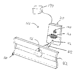
Figure 1 shows a perspective view of a diffractive optical encoder 100
constructed
according to the invention. As shown, encoder 100 includes three basic
components: an
opto-electronic assembly, or sensor head, 110, a scale 160, and a signal
processor 190.
Figure 2A shows a side view of encoder 100. Figure 2B shows a view of the
sensor head 110 taken in the direction of line 2B-2B as shown in Figure 2A.
Figure 2C
shows a view of the scale 160 taken in the direction of line 2C-2C as shown in
Figure 2A.
Figure 2D shows an end view of encoder 100 taken in the direction of line 2D-
2D as
shown in Figure 2A. For convenience of illustration, signal processor 190 is
not shown in
Figures 2A-2D.
With reference to Figures 1 and 2A-2D, the sensor head 110 includes a light
source 112, a primary detector array 120, and an index, or reference point,
detector 140.
As shown, the source 112 and the detectors 120, 140 are all mounted on a
common
substrate 111. Primary detector array 120 and index detector 140 are
preferably
implemented on a single piece of silicon. The scale 160 includes a substrate
161 upon
which is disposed a diffractive grating 162 and two diffractive optical
elements (DOES)
166. The scale 160 is generally disposed opposite the sensor head 110 so that
they are
separated by a fixed distance d (as shown in Figure 2D), and so that the scale
160 and the
sensor head 110 may move relative to one another in the direction indicated by
the arrow
A-A shown in Figure 2A. In operation, the encoder 100 monitors movement of the
scale
160 relative to the sensor head 110 (in the direction of arrow A-A), and
generates a signal
representative of the position of scale 160 relative to sensor head 110.
In operation, light source 112 emits an expanding, or diverging, cone of light
102.
Source 112 is preferably a source of quasi-monochromatic light (or nearly
monochromatic light) and may be implemented using a vertical cavity surface
emitting
laser (VCSEL). As shown in Figure 1, the sensor head 110 and scale 160 are
preferably
disposed so that when the light cone 102 reaches scale 160, the light cone 102
is wide
enough to be incident on a portion of the grating 162 as well as one of the
DOEs 166.
Some of the light in cone 102 propagates through, and is diffracted by, scale
160, and this
light preferably does not return towards the sensor head 110. Also, some of
the light in
cone 102 is reflected and diffracted back towards sensor head 110. The sensor
head 110
-4-
BOSTON 1477263v1
CA 02458954 2004-02-27
WO 03/021194 PCT/US02/25446
and the scale 160 are preferably configured so that (1) light diffracted from
grating 162
back towards the sensor head 110 is incident primarily on detector array 120
and (2) light
diffracted from the DOE 166 back towards the sensor head 110 is incident
primarily on
the index detector 140. As will be discussed in greater detail below, light
incident on
detector array 120 allows encoder 100 to provide a relative measurement of the
position
of sensor head 110 relative to scale 160, whereas light incident on index
detector 140
allows encoder 100 to provide an index point measurement, or reference point
measurement, of the position of sensor head 110 relative to scale 160.
Figures 3A, 3B, and 3C show the scale 160 in more detail. Specifically,
Figures
3B and 3C show expanded versions of the region 310 shown in Figure 3A. The
scale 160
is preferably formed on a glass-like substrate 161. The grating 162 may be
composed of
alternating optically reflecting stripes 164 and optically transmitting
stripes 163 as shown
in Figure 3B. The reflecting stripes 164 are preferably formed by coating
regions of
substrate 161 with a highly reflecting material. In this embodiment, the
transmitting
stripes 163 are formed simply by leaving the substrate 161 uncoated.
Alternatively,
optically absorbing stripes could be used in place of the transmitting
stripes. As shown in
Figure 3C, in another embodiment, the stripes could all be reflecting and
alternating
stripes could be disposed at different depths. A grating 162 of the type shown
in Figure
3B is known as an "amplitude grating". A grating 162 of the type shown in
Figure 3C is
known as a "phase grating".
Regardless of whether the grating 162 is implemented as shown in Figure 3B or
3C, each stripe is preferably a thin rectangle oriented with its short
dimension parallel to
the displacement direction of the scale (i.e., parallel to the arrow A-A shown
in Figure 1).
The center-to-center spacing of the stripes (or left edge to left edge spacing
of the stripes,
as is shown in Figures 3B and 3C) defines the period P of the grating 162.
Preferably, the
stripes are equally spaced and the short dimension of each stripe is
substantially equal to
one-half of the grating's 162 period P. Depending on the desired system
performance, the
period P typically is between 5 and 40 microns, with 20 microns being a
preferred value.
Ideally, the scale is anti-reflection coated on the exposed glass regions on
both sides of
the scale.
-5-
BOSTON 1477263v1
CA 02458954 2004-02-27
WO 03/021194 PCT/US02/25446
Returning to Figure 1, grating 162 diffracts light from cone 102 into multiple
cones of light that are directed towards the sensor head 110. Figure 4, which
is a view of
encoder 100 in the same orientation as shown in Figure 2A, illustrates some of
the cones
of light 103 diffracted by grating 162 towards the sensor head. The cones 103
of
diffracted light optically interfere with one another and generate complex
fringe-like
patterns in the space between the scale 160 and the sensor head 110.
Figure S schematically illustrates the intensity of the fringe patterns formed
by
interference between diffracted light cones 103 at different distances away
from the
grating 162. As shown, at distances d2 and d4 away from the grating 162, the
optical
fringe pattern generated by interference between light cones 103 is a
relatively high
contrast periodic pattern. Conversely, at distances dl and d3 away from the
grating 162,
the optical fringe pattern is relatively low contrast. The planes at distances
d2 and d4
away from the grating 162 may be referred to as self-imaging planes, or
"Talbot (or
talbot) imaging planes". At these talbot imaging planes, the diverging cones
of diffracted
light combine with the same relative phases they had at the grating and
essentially form
an image of the grating 162 itself. As is discussed generally in U.S. Pat. No.
5,991,249,
these high contrast imaging planes regularly occur and the distance between
the grating
and any of these imaging planes may be calculated according to the following
Equation
(1).
zozl _ NP2 (1)
(zo+zl)
In Equation (1), zo equals the distance between light source 112 and grating
162,
z~ equals the distance between grating 162 and the talbot self imaging planes,
N is an
integer, P is the period of the grating, and ~. is the wavelength of light
emitted by source
112.
As shown in Figure 5, the first talbot plane (at distance d2 away from the
scale) is
one hundred eighty degrees out of phase with the second talbot plane (at
distance d4 away
from the scale). In general, adjacent talbot planes are one hundred eighty
degrees out of
phase with each other. The reason for this one hundred eighty degree phase
shift between
-6-
BOSTON 1477263v1
CA 02458954 2004-02-27
WO 03/021194 PCT/US02/25446
adjacent talbot planes is that at even planes (i.e., talbot planes for which N
is equal to an
even number), all orders of diffracted light combine with the same relative
phases they
had at the grating, whereas at odd planes (i.e., talbot planes for which N is
equal to an odd
number), the zeroth order is one hundred eighty degrees out of phase and all
other orders
combine with the same relative phases they had at the grating.
It should be noted that the patterns illustrated in Figure 5 are
characteristic of the
fringe patterns generated when the wroth order beam contributes to the pattern
(e.g.,
when the fringe pattern is formed by interaction between the zeroth order,
plus first order,
minus first order, as well has other higher order diffracted beams). If the
zeroth order
beam were eliminated, then the fringe patterns would look significantly
different from
those illustrated in Figure 5. Specifically, in the case of a phase grating
with'/2-
wavelength delays, the planes of low contrast are the Talbot imaging planes
and the
planes of high contrast are between the Talbot imaging planes. In the regions
of high
contrast, the fringe patterns do not appear as images of the original grating,
as is the case
with an amplitude grating. Rather, the fringe patterns for the phase grating
are generally
a complicated combination of harmonic components, usually dominated by a
component
with a period generally one half that of the period illustrated in the talbot
planes of Figure
5. As with the amplitude grating, the period of the fringe pattern from a
phase grating
increases in proportion to the distance from the scale. In general, it is
difficult to predict
the planes in which the fringe pattern from a phase grating will exhibit the
least harmonic
distortion and/or noise.
Accordingly, elimination of the wroth order beam may be regarded as causing
degradation of the periodic signal that is monitored by the encoder. However,
it may still
be advantageous to construct encoders in which the wroth order beam is
eliminated for at
least the following reason; as a practical matter, in an encoder of the design
of the present
invention, the higher diffracted orders are quickly filtered out by
propagation and the
resulting fringe patterns often approach pure sinusoidal forms.
Notwithstanding the above benefit of phase gratings, the preferred grating for
this
invention is an amplitude grating. Amplitude gratings (as shown in Figure 3B)
are much
BOSTON 1477263v1
CA 02458954 2004-02-27
WO 03/021194 PCT/US02/25446
more widely available commercially than phase gratings (as shown in Figure
3C).
Therefore, designing an encoder that uses an amplitude grating is advantageous
because it
is less expensive and generally easier to acquire the scale. However, use of
an amplitude
grating does imply the presence of the zeroth order beam. The design of
encoders in
which the zeroth order beam is present will now be discussed.
In encoders constructed according to the invention, the sensor head 110 and
scale
160 are preferably disposed so that detector array 120 lies in one of the
talbot imaging
planes (i.e., so that the distance between the scale and the sensing surface
of the detector
array is equal to z1 as calculated according to the above Equation (1)). As is
apparent
from Figures 2A and 2D, in encoders constructed according to the invention,
the upper
light emitting surface of source 112 is preferably substantially coplanar with
the upper, or
sensing, surface of detector array 120. So, in encoders constructed according
to the
invention, the distance zo is substantially equal to the distance z1. In the
case where zo
equals z1, the above Equation (1) reduces to the following Equation (2).
.:o -~ 2 ~Pi -
(2),
So, to insure that the detector array 120 is disposed in one of the talbot
imaging
planes, in encoders constructed according to the invention, the distance d (as
shown in
Figure 2D) between the sensor head 110 and the scale 160 is preferably
adjusted so the
separation between the scale 160 and the detector array 120 is substantially
equal to zo as
calculated by Equation (2) for some integer value of N. However, since it is
almost
impossible to insure that the actual distance between the scale 160 and the
detector array
120 is exactly equal to zo, this distance is preferably selected so that the
sensing surface of
the detector array 120 lies in a region near one of the talbot planes. The
desired size of
this region will now be discussed.
As shown in Figure 5, the distance between the scale and the first talbot
plane is
d2. In addition, the distance between the scale and the nth talbot plane is
nd2 (i.e., n times
d2). If it is desired to locate the detector array at the nth talbot plane,
then the distance
between the scale and the detector array is preferably equal to nd2 plus or
minus O.Sd2.
So, for example, if it is desired to locate the detector array at the third
talbot plane, then
_g_
BOSTON 1477263v1
CA 02458954 2004-02-27
WO 03/021194 PCT/US02/25446
the detector array should be placed within the region extending from 2.Sdz
away from the
scale to 3.Sdz away from the scale. Continuing this example, if the space
between the
scale and the detector array is equal to 3.Odz, then the detector array will
lie exactly in the
third talbot plane. If this distance is slightly greater or less than 3.Odz,
then the contrast of
the fringe pattern will be slightly less than optimal and accuracy of the
encoder will
correspondingly be slightly decreased. As the detector array is moved further
from the
desired location of 3.Odz, contrast of the fringe pattern will continue to
decrease until the
contrast reaches a minimal value at the distance 2.Sdz or 3.Sdz (i.e., the
contrast will be at
minimal value at these locations because the talbot planes are separated by
evenly spaced
planes characterized by minimal contrast). Since the talbot planes are
separated by
evenly spaced planes of minimum contrast, ndz plus or minus O.Sdz denotes the
maximum
size of the range within which the detector array should be located.
Performance of an
encoder will increase if the detector array is located ndz plus or minus 0.2dz
away from
the scale, and performance of the encoder will increase still further if the
detector array is
located ndz plus or minus 0.1 dz away from the scale. More generally, the
detector array
120 preferably lies in a region bounded by two planes, where the first plane
is separated
from the scale by ndz plus xdz, and the second plane is separated from the
scale by ndz
minus xdz, where x is less than or equal to one half. One preferred value for
x is 0.2, and
a more preferred value for x is 0.1.
As noted above, if the zeroth order beam is eliminated, then a high contrast
fringe
pattern may be incident on the detector array regardless of the spacing
between the
detector array and the scale. Accordingly, it may be advantageous to alleviate
the above-
discussed restrictions on spacing between the detector array and scale by
using a scale
160 that has a phase grating (as shown in Figure 3C) that substantially
eliminates the
zeroth order beam. In such an embodiment, the distance between the upper
stripes and
the lower stripes (or the depth of the lower stripes) is preferably
substantially equal to N
quarter-wavelengths of the light produced by light source 112, where N is an
odd integer.
Another advantage of using such a phase grating is that it reduces the period
of the optical
fringe pattern by a factor of two and thereby potentially increases the
resolution of the
encoder by a factor of two. Alternatively, if it is desired to produce an
encoder using a
-9-
BOSTON 1477263v1
CA 02458954 2004-02-27
WO 03/021194 PCT/US02/25446
phase grating in which the zeroth order beam is present, then the distance
between the
upper stripes and the lower stripes is preferably substantially equal to (N+x)
times one
quarter of the wavelength of the light produced by light source 112, where N
is an odd
integer, and where x is a small number that is less than one half.
As shown in Figure 5, the interference fringes are periodic and are
characterized
by a period T. Since the grating 162 is illuminated by an expanding cone of
light, the
period T of the fringes is in general a function of the distance away from the
grating as
shown in the following Equation (3).
T-(zo+zl)*P-(2zo+e)*P-KP (3)
zo zo
In Equation 3, zo is the optical path length between the light source 112 and
the
scale 160, z, is the optical path length between the scale and the detector
array 120, P is
the period of the grating, a is the offset between the light source 112 and
the detector
array 120 (i.e., or the difference between zo and z1), and K is the scale
factor.
As may be seen from Equation (3), in the special case in which the distance
between the light source and the grating (zo) is equal to the distance between
the detector
array and the grating (z1) (viz., a is zero), the scale factor K is 2 so the
period T of the
interference fringes is always equal to a constant value which is twice as
large as the
period of the grating P (i.e., T=2P). Since, as discussed above, the upper
light emitting
surface of source 112 is preferably substantially coplanar with detector array
120, in
encoders constructed according to the invention, the distance between the
light source and
the grating (z0) is substantially equal to the distance between the grating
and the detector
array (z1). Accordingly, in encoder 100, the period T of the fringes incident
on detector
array 120 is always substantially equal to the constant 2P.
In operation, movement of the scale 160 relative to the sensor head 110 in the
direction of arrow A-A as shown in Figure 2A causes the fringe pattern
incident on
detector array 120 to move across the detector array 120 in the direction of
arrow A-A.
Movement of the incident fringe pattern across the detector array is
equivalent to a
change in the phase angle between the incident fringe pattern and the detector
array.
- L0 -
BOSTON 1477263v1
CA 02458954 2004-02-27
WO 03/021194 PCT/US02/25446
Detector array 120 and the associated signal processor 190 monitor this phase
angle and
thereby monitor the position of the sensor head 110 relative to the scale 160.
Detector array 120 is preferably constructed as an array of photodetectors
configured to facilitate measurement of the phase angle between the detector
array and
the fringe pattern incident on the detector array. Copending U.S. Patent
Application
Serial No. 60/316,121, entitled HARMONIC SUPPRESSING PHOTODETECTOR
ARRAY [Attorney Docket No. MCE-018 (111390-140)], which was incorporated by
reference above, discloses several detector arrays which may be used to
implement
detector array 120. However, any detector array that permits measurement of
the phase
angle between the array and the incident fringe pattern may be used to
implement array
120. The output signals generated by detector array 120 are applied to signal
processor
190. Signal processor 190 preferably generates an output signal representative
of the
phase angle between the array 120 and the fringe pattern incident on array
120.
Figure 6 shows a view of the top of sensor head 110 similar to the view shown
in
Figure 2B, however, Figure 6 shows additional detail. As shown, detector array
120
includes a plurality of rectangular photodetectors, each of which has a long
axis extending
in the direction of the line L-L (i.e., along the length of the photodetector)
and a short axis
extending in the direction of the line W-W (i.e., along the width of the
photodetector).
Detector array 120 is preferably configured for use with the 4-bin algorithm
and
photodetectors in the array are accordingly, preferably electrically connected
to four
bonding pads 121. Processing circuitry 190 (not shown) is electrically
connected to
bonding pads 121 to permit monitoring of array 120. Light source 112 is
preferably
electrically connected to, and controlled by electrical signals applied to,
two bonding pads
113. The aperture 114 of VCSEL 112, through which all light emitted by the
VCSEL
passes is also shown in Figure 6.
As is also shown in Figure 6, index detector 140 is preferably implemented in
a
tri-cell configuration that includes a central photodetector 142 and two end
photodetectors
144 disposed on either side of the central photodetector 142. The central
photodetector
142 is electrically connected to a bonding pad 143. Each of the end
photodetectors 144 is
electrically connected to a bonding pad 145. Processing circuitry 190 (not
shown in
-11-
BOSTON 1477263v1
CA 02458954 2004-02-27
WO 03/021194 PCT/US02/25446
Figure 6) is electrically connected to bonding pads 143, 145 to permit
monitoring of
index detector 140. The central detector 142 is preferably aligned with light
source 112
so that a line extending from aperture 114 parallel to the line L-L will
bisect the central
detector 1.42.
Referring to Figure 1, the diverging light cone 102 emitted by light source
112 is
shown as illuminating DOE 166. It will be appreciated that DOE 166 will move
into and
out of light cone 102 as the scale 160 and sensor head 110 are moved with
respect to one
another in the direction of the arrow A-A as shown in Figure 2A. When DOE 166
is
illuminated by light cone 102, the DOE 166 diffracts light from cone 102
towards index
detector 140. DOE 166 is preferably implemented using an anamorphic zone plate
lens.
When it is illuminated by light cone 102, DOE 166 preferably generates a "line
image" of
the light source 112. That is, DOE 166 preferably diffracts a "line of light"
back towards
index detector 140. The line image generated by DOE 166 and incident on sensor
head
110 is preferably substantially parallel to the line L-L as shown in Figure 6.
For clarity, only one DOE 166 is shown in the scale 160 in Figure 1. However,
as
shown in Figures 2C and 3A, scale 160 may include two DOEs 166 disposed on
either
side of the grating 162. The cone of light 102 that reaches scale 160 is
preferably large
enough to illuminate a portion of the grating 162 and only one of the DOES
166.
However, if two DOEs 166 are included on scale 160, the scale 160 and the
sensor head
110 may be assembled without regard to orientation when forming encoder 100.
That is,
if scale 160 includes two DOEs 166, regardless of whether the scale 160 is
installed right
side up or up side down, one of the DOEs 166 will be illuminated by the light
cone 102.
It will of course be appreciated that scale 160 can also be built using only
one DOE 166.
Also, scale 160 can include two DOES 166 that are not disposed symmetrically
(e.g., one
DOE may be disposed near the center of the scale and another DOE may be
disposed near
an end of the scale).
In operation, as scale 160 and sensor head 110 are moved with respect to one
another (in the direction of line A-A as shown in Figure 2A), the line image
generated by
DOE 166 will sweep across the index detector 140. Movement of the scale 160
relative
to the sensor head 110 in the direction of line A-A by a distance D causes the
line image
- 12-
BOSTON 1477263v1
CA 02458954 2004-02-27
WO 03/021194 PCT/US02/25446
generated by DOE 166 to move across sensor head 110 by a distance equal to KD,
where
K is the scale factor from equation 3. So, for the case in which a is zero
(i.e., where zo
equals z1, as described in Equation (3)), as the scale 160 is displaced
relative to the sensor
head 110, the line image generated by DOE 166 moves across the sensor head 110
at
twice the rate of movement of the scale. The line image generated by DOE 166
will be
centered on the central photodetector 142 of index detector 140 only when the
DOE 166
is directly over the light source 112 (i.e., when the encoder is configured as
shown in
Figure 1). Processing circuitry 190 generates an output signal representative
of the light
incident on index detector 140. This output signal may be called an index
signal.
Preferably, the index signal is characterized by a pulse every time the line
image
generated by DOE 160 sweeps across the index detector 140. It will be
appreciated that
such a pulse provides an index point, or reference point, measurement of the
relative
orientations of scale 160 and sensor head 110. The measurement of distance, or
displacement, between scale 160 and sensor head 110 generated by detector
array 120 is a
relative measurement because the fringe pattern incident on array 120 is a
periodic signal.
However, the line image generated by DOE 160 will only be incident on index
detector
140 when the light source 112, the DOE 160, and the index detector 140 are all
in a
particular orientation, and that is why the index signal provides a reference
measurement.
Processing circuitry 190 may use a variety of algorithms for generating the
index
signal. Preferably, processing circuitry 190 uses an algorithm that is
insensitive to
variations in the output signals generated by index detector 140 that may be
caused by
light source intensity variations, stray light, and misalignments of the
sensor head 110 and
the scale 160. The index signal is preferably characterized by a pulse
whenever the line
image diffracted by DOE 166 sweeps across the index detector 140 and the width
of that
pulse is preferably substantially equal to the period P of grating 162. Such a
pulse width
allows the pulse to uniquely identify, or correspond with, a single fringe of
the pattern
generated by grating 162. In one preferred embodiment, the width of the
central
photodetector 142 (as measured in the direction of the line W-W as shown in
Figure 6) is
substantially equal to twice the period P of the grating 162. In this
embodiment, the index
-13-
BOSTON 1477263v1
CA 02458954 2004-02-27
WO 03/021194 PCT/US02/25446
signal is preferably high whenever the center of the line image generated by
DOE 166 is
incident on the central photodetector 142 and is preferably low at all other
times.
Figure 7 illustrates the general shape of the output signals generated by
index
detector 140 when a line image 700 moves across the array in a left to right
direction as
indicated by arrow 702. The curve A shows the shape of the output signal
generated by
the left end photodetector 144 as line image 700 moves over the photodetector.
The
curve B shows the shape of the output signal generated by the central
photodetector 142
as line image 700 moves over the photodetector. Finally, the curve C shows the
shape of
the output signal generated by the right end photodetector 144 as line image
700 moves
over the photodetector. One preferred method of generating the index signal
from the
raw output signals A, B, and C is for processing circuitry 190 to generate the
two signals
S1 and S2 according to the following Equation (4).
S1 =-A+2B-C (4)
S2 = A-2B+C
Figure 7 also shows the signals S1 and S2 generated according to Equation (4)
from the raw signals A, B, and C shown in Figure 7. It will be apparent from
Equation
(4) that both signals S1 and S2 are independent of stray light because any
light that is
incident on all three photodetectors of index detector 140 will be subtracted
out, or will
not contribute to S1 and S2.
As shown, the signal S1 generally contains a positive peak when the center of
line
image 700 is incident on the central photodetector 142. In addition, signal S1
contains a
number of sidelobes, or ringing, traceable to the inherent diffraction effects
in the line
image. Similarly, the signal SZ generally contains a negative peak when the
center of line
image 700 is incident on the central photodetector 142, and a number of
sidelobes from
the diffraction effects in the line image. One preferred method of generating
the index
signal from the signals S1 and SZ is shown in the following Equation (5).
index signal - 1 when Sl > (S2 + O) (5)
0 otherwise
-14-
BOSTON 1477263v1
CA 02458954 2004-02-27
WO 03/021194 PCT/US02/25446
In Equation (5), O is a constant offset that is preferably greater than the
expected
sidelobe peaks in S, and S2 and is also preferably less than the smallest
expected
maximum value of S~.
Figure 7 also shows an index signal generated according to Equation (5). As
shown, this index signal has the desired characteristic of being equal to a
one, or a high
value, whenever the center of the line image generated by DOE 166 is incident
on the
central photodetector 142 and is equal to zero, or a low value, at all other
times. Such an
index signal will be characterized by a pulse whenever the line image
generated by DOE
166 sweeps across the index detector 140.
While use of Equation (5) is a preferred method of generating the index
signal, it
will be appreciated that other approaches could be used as well. For example,
the index
signal could simply be set to a high value whenever the signal S1 is greater
than a selected
constant value.
The widths of the end photodetectors 144 are preferably equal to the width of
the
central photodetector 142. This insures that stray light will not contribute
to the signals
S1 and S2. However, it will be appreciated that in other embodiments, the
width of the
end photodetectors 144 could be different than the width of the central
photodetector 142.
One advantage to using end photodetectors 144 that are of different widths
than the
central photodetector 142 is that such a configuration can reduce the
sidelobes of the
signals S1 and S2 by effectively averaging out the diffraction effects in the
line image.
Also, adjusting the detector widths and/or spacings can allow the ringing in
the signals
from the end photodetectors to cancel out the ringing in the signal from the
central
photodetector. If such an approach is used, the weighting of the raw signals
in Equation
(4) is preferably altered so that the signals S1 and S2 are still insensitive
to stray light. In
yet other embodiments, the index detector 140 could be constructed by using
only the
central detector 142 and by eliminating the end detectors 144. However, such
an
approach is not preferred because the resulting index signal becomes too
sensitive to
noise and misalignments.
Figure 8 shows yet another embodiment of index detector 140. In this
embodiment, detector 140 includes two bi-cell detectors 140A and 140B. Bi-cell
140A
-15-
BOSTON 1477263v1
CA 02458954 2004-02-27
WO 03/021194 PCT/US02/25446
includes a center detector 142 and a left end detector 144. Bi-cell 140B
includes a center
detector 142 and a right end detector 144. The two bi-cells are preferably
positioned so
that a line extending from light source 112 in the direction of the line L-L,
as shown in
Figure 6, would bisect the center detectors 142 of both bi-cells 140A and
140B. It will be
appreciated that the signals S1 and S2 may easily be generated according to
the above
Equation (4) using bi-cell detectors 140A, 140B. For example, the signal Sl
may be
generated simply by adding the output signals generated by the two central
detectors 142
together and subtracting from that sum the output signals generated by the two
end
detectors 144.
Figure 9 shows an end view of a preferred embodiment of a diffractive optical
encoder 100 constructed according to the invention. Figure 9 shows a view of
the
encoder 100 taken in the direction of line 2D-2D as shown in Figure 2A. The
principal
difference between Figure 2D and Figure 9 is that in Figure 9 the sensor head
1 L0 is
shown tilted with respect to (instead of substantially parallel to) grating
160. More
specifically, the sensor head 110 is tilted about an axis that is
substantially parallel to the
direction of travel of the scale 160 (i.e., parallel to the line A-A as shown
in Figure 2A).
Preferred embodiments of encoder 100 include a tilt as shown in Figure 9.
Tilting the
sensor head 110 with respect to the grating 160 as shown in Figure 9 provides
at least two
advantages. First, it reduces the amount of light that reflects from the scale
160 back into
the light source 112. Second, it increases and balances the amount of light
that reaches
detector array 120 and index detector 140.
Generally, it is undesirable for light reflected from the scale to enter the
light
source 112. First, even the preferred VCSEL light sources are detrimentally
affected by
reflected light that re-enters the lasing medium. Second, since the emitting
surface of a
laser is somewhat reflective, any light that reaches this surface will be
reflected back
towards the scale 160. This multiply reflected and/or diffracted stray light,
if not properly
controlled, can cause extraneous components in the detected signals. In the
present
invention, the intentional tilt between the optoelectronics plane and the
scale has been
selected to direct these extraneous beams away from the detectors. Tilting the
sensor
head 110 relative to the scale as shown in Figure 9 effectively (I ) prevents
light reflected
-16-
BOSTON 1477263v1
CA 02458954 2004-02-27
WO 03/021194 PCT/US02/25446
from the scale from re-entering the light source 112, or significantly reduces
the amount
of such light and (2) insures that light reflected off of the light source
does not reach the
detectors, or significantly reduces the amount of such light.
The second function of introducing a tilt between the sensor head 110 and the
scale 160 is to increase and balance the light levels reaching the detectors.
The sensor
head 110 is preferably tilted so as to place the peak intensity of the
specularly reflected
cone of light nearly half way between detector array 120 and index detector
140. This
maximizes the amount of light that is incident on the two detector regions
120, 140, while
minimizing the fall-off of light intensity on both regions.
As discussed above, it is advantageous to construct encoder 100 so that the
optical
path length between light source 112 and scale 160 is substantially equal to
the optical
path length between scale 160 and the detector array 120. Doing so insures
that the
period of the fringe pattern incident on detector array 120 is independent of
the distance
between the sensor head 110 and the scale 160. When light source 112 is
implemented as
a VCSEL that emits light in a direction perpendicular to the plane of sensor
head 110 (as
illustrated in Figure 1), equalizing these optical path lengths can be
achieved by making
the top surface of detector array 120 coplanar with the emitting surface of
light source
112. However, since light sources and photodetectors are each typically
characterized by
a particular thickness, it can be difficult in practice to make these surfaces
coplanar.
Figure 10A shows one technique for making these surfaces coplanar. As shown in
Figure 10A, a trench 900 has been etched into the substrate 111 of sensor head
110.
Either the photodetectors of detector array 120 or the light source 112 may be
disposed
inside trench 900 as indicated by the box 910. It will be appreciated that
using such a
trench can compensate for differences in the thickness of the detector array
120 and the
light source 112. A trench such as trench 900 may be provided either by
machining
substrate l l l or by using photolithographic techniques.
Figure lOB shows another technique for making these surfaces coplanar. As
shown in Figure l OB, a spacer 912 has been disposed on the upper surface of
substrate
111 of sensor head 112. As indicated by the box 910, either the photodetectors
of
detector array 120 or the light source 112 may be disposed on such a spacer.
Spacers
-17-
BOSTON 1477263v1
CA 02458954 2004-02-27
WO 03/021194 PCT/US02/25446
such as spacer 112 of desired thickness may be formed on substrate 111 for
example by
material deposition or by adhering a previously formed spacer to the top of
substrate 11 l..
Figures lOC and lOD illustrate how the light source 112 can be implemented
using an edge emitting laser diode instead of a VCSEL and also illustrate
other strategies
for equalizing the optical path length between the light source 112 and the
scale 160 and
the optical path length between the scale 160 and the detector array 120. In
Figure IOC,
the light source 112 is implemented using an edge emitting laser diode that
emits light in
a direction basically parallel to the upper surface of sensor head 110. In
this embodiment,
sensor head 110 also includes a reflecting mirror 920 disposed in the optical
path of
source 112. Mirror 920 reflects the cone of light emitted by source 112 up
towards the
scale (not shown). In Figure IOD, the light source 112 is again implemented
using an
edge emitting laser diode. In this embodiment, the light source is disposed in
a trench
900 that has been provided in the substrate 111 of sensor head 110. One edge
930 of
trench 900 has been made reflecting so that edge 930 reflects the cone of
light emitted by
source 112 up towards the scale (not shown). It will be appreciated that
mirror 920 or
reflective edge 930 may be implemented using reflective prisms or etched fold
mirrors as
described in U.S. Patent No. 6,188,062. The arrangements illustrated in
Figures lOC and
lOD each affect the optical path length between the light source 112 and the
scale. It will
be appreciated that such arrangements can be used to equalize the optical path
length
between the source 112 and the scale and the optical path length between the
scale and
the detector array 120.
Alternatively, to avoid the cost of using trenches or spacers as suggested in
Figures l0A-lOD to equalize the optical path between the light source 112 and
the scale
160 (zo) and the optical path between the scale 160 and the detector array 120
(z1), the
notion of having equal optical path lengths, and a fringe period that is
independent of the
distance between the scale and the detector array, can be abandoned. In such a
case, the
period T of the fringes incident on detector array 120 are proportional to the
period P of
the grating and are given by the above Equation (3). When designing such an
encoder, it
is desirable to calibrate the scale factor between the scale and the detector
array and to
optimize the encoder accordingly.
-18-
BOSTON 1477263v1
CA 02458954 2004-02-27
WO 03/021194 PCT/US02/25446
In the ideal case, where z0 equals z~, and there are no other misalignments,
the
encoder scale factor is substantially equal to two (i.e., because the period T
of the fringes
incident on the detector array are substantially equal to two times the period
P of the
grating). However, in practice the actual scale factor associated with optical
encoders
constructed according to the invention tends to be close, but not exactly
equal, to two.
One principal reason that the scale factor is generally not exactly equal to
two is that is it
difficult to measure components accurately enough and to fabricate
spacers/trenches
precisely enough to make zo exactly equal to z1. Also, other factors, such as
misalignments, contribute to perturbing the scale factor from the ideal value
of two.
Finally, the preferred scale factor for an optical encoder is the one which
provides the
highest accuracy performance, without direct regard to the actual value of the
fringe or
detector periods.
Given this criterion (best accuracy), a preferred method for determining the
scale
factor of an optical encoder constructed according to the invention and then
calibrating
that encoder in view of the measured scale factor will now be discussed.
Preferably, a
calibration sensor head and a calibration scale are produced. The calibration
scale has a
calibration grating similar to grating 162, however, rather than being
characterized by a
substantially uniform period (as grating 162 preferably is), the calibration
grating includes
several different sections, each section being characterized by a unique
period. One
section is fabricated with the design period P (e.g., P equal to 20 microns).
Other sections
are characterized by periods that deviate slightly from P. Preferably, the
various sections
of calibration grating span a range of periods around P in incremental steps
of
approximately 0.5% of P. That is, the various sections have periods that are
approximately P, 0.995P, 1.OOSP, 0.990P, etc. The inventors have observed that
a range
of periods of +/- 3% typically includes the optimum period. Of course, as will
be obvious
to one skilled in the art, should the best performance be observed at an end
point of the
range, then a new calibration grating should be produced with a wider range.
The various
sections of the calibration should be distributed spatially on a common
substrate and be
separated enough for easy identification and selection. For ease of use and
alignment, the
axes of the various sections should all be parallel. The calibration sensor
head includes a
- 19-
BOSTON 1477263v1
CA 02458954 2004-02-27
WO 03/021194 PCT/US02/25446
calibration detector array that is preferably configured (e.g., using one of
the methods
described in the above-identified U.S. Patent Application Serial No.
60/316,121, entitled
HARMONIC SUPPRESSING PHOTODETECTOR ARRAY [Attorney Docket No.
MCE-018 (111390-140)]) to measure the phase angle of a fringe pattern incident
on the
array that has a period T substantially equal to the design point, 2P. The
calibration
sensor head and the calibration scale are then configured to form a
calibration encoder
(e.g., as shown in Figures 2A-2D).
If the encoder scale factor of the calibration encoder were exactly equal to
two
(and there were no other perturbing effects), then the calibration encoder
would provide
the most accurate results when the calibration detector array were used with
the section of
the calibration grating characterized by a period of P. However, normally, the
most
accurate results will actually be provided when the calibration detector array
is used with
some other section of the calibration grating. The calibration encoder is
preferably tested
using each of the sections of the calibration grating to determine which
section of the
calibration grating provides the most accurate results. Typically, the
accuracy of each test
is judged by the rms difference between the encoder output and a displacement
truth
sensor that has made simultaneous measurements of the grating motion. A laser
interferometer has been used successfully as the truth sensor.
Since the calibration encoder was designed to operate with a grating with a
period P, but the most accurate results are generally obtained from the
calibration grating
section having a period FP, accordingly, it can be assumed that the measured
calibration
factor, F, should be used during the manufacture of the operational encoder.
Specifically,
the operational encoder should either use a grating with a period FP or the
detector array
period T should be modified to be T/F.
At this point, encoders can be manufactured in large numbers according to the
invention by using scales 160 in place of the calibration scale and by using
sensor heads
1 L0 in place of the calibration sensor head. One method of constructing
encoders
according to the invention is to use (1) scales having gratings 162
characterized by a
period of FP and (2) sensor heads having detector arrays 120 configured for
measuring
-20-
BOSTON 1477263v1
CA 02458954 2004-02-27
WO 03/021194 PCT/US02/25446
the phase angle of an incident fringe pattern characterized by a period T
substantially
equal to 2P. One problem with this approach is that the resulting period FP of
the grating
162 is unlikely to be an integer number of standard length units (viz.,
microns or mils).
Thus, for example, the grating period of such a grating might be 20.2 microns
instead of a
more typical 20 microns. Accordingly, a preferred approach for constructing
encoders
according to the invention is to use (1) gratings 162 characterized by a
period of P and (2)
sensor heads having detector arrays 120 configured for measuring the phase
angle of an
incident fringe pattern having a period substantially equal to 2P divided by
the scale
factor F. This latter approach is preferred because it allows any generation
of sensor
heads constructed according to the invention to be used interchangeably with
industry
standard scales.
If an index detector 140 is included in the encoder, it will be appreciated
that it
may also be desirable to adjust the width of the index detector elements
according to the
calibration scale factor. For example, it may be advantageous to make the
width of the
central photodetector of index detector 140 substantially equal to the period
P of the
grating 162 divided by the scale factor F.
Figures 11A and 11B illustrate an additional feature that may be incorporated
into
encoders constructed according to the invention. Figures 11A and 11B each show
a side
view of a diffractive optical encoder 100 taken from the same perspective as
Figure 2A.
Figure 1 1A shows the diverging cone of light 102 extending from the sensor
head 110 up
towards the scale 160. Figure 1 1A also illustrates three beams of light that
have been
diffracted by grating 162 of scale 160 down towards detector array 120.
Specifically,
Figure 11A shows the zeroth order beam, the left and right boundaries of which
are
indicated by reference characters 1000; the minus first order beam, the left
and right
boundaries of which are indicated by reference characters 1001; and the minus
third order
beam, the left and right boundaries of which are indicated by reference
characters 1003.
As shown, the wroth, minus first, and minus third order beams are all incident
on detector
array 120. It will be appreciated that other beams (e.g., the positive first
and third, as well
as the positive and negative fifth order beams) are also incident on detector
array 120,
however, for convenience of illustration, these beams are not shown in Figure
10A. One
-21-
BOSTON 1477263v1
CA 02458954 2004-02-27
WO 03/021194 PCT/US02/25446
problem with the encoder shown in Figure 11A is that a large number of
diffracted beams
are all incident on detector array 120 and the presence of these beams can
degrade the
quality of the resulting interference pattern that is incident on the detector
array 120.
The encoder 100 shown in Figure 11B is similar to the one shown in Figure 11
A,
however, the Figure 11B encoder additionally includes a mask 1010. As shown,
the mask
1010 is disposed close to scale 160, between sensor head 110 and scale 160.
Mask 1010
also defines a central aperture 1012. Mask 1010 prevents most of the light in
cone 102
from reaching scale 160. That is, only light passing through aperture 1012
reaches scale
160. Mask 1010 is preferably fabricated from an absorbing material so that
light incident
on mask 1010 is simply absorbed and is not reflected back towards the sensor
head 110.
Mask 1010 advantageously restricts the angular extent of the beams that are
diffracted by
scale 160 back towards the sensor head 110. In the encoder illustrated in
Figure 11B, the
zeroth and minus first order beams are incident on detector array 120,
however, the minus
third order beam is not incident on the detector array 120. It will be
appreciated that if
the third order beams are not incident on detector array 120, then all higher
order beams
will also not be incident on the detector array (i.e., the higher order beams
will be
displaced even more to the left or right of the detector array 120 than is the
illustrated
minus third order beam). Mask 1010 accordingly advantageously improves the
quality of
the interference pattern incident on detector array 120 by removing unwanted
higher
order beams. In operation, mask 1010 and sensor head 110 preferably remain
fixed
relative to one another, and the scale 160 is moved (to the left and right in
the
configuration illustrated in Figure 11B) with respect to the sensor head 110.
As is discussed in the above-identified U.S. Patent Application Serial No.
60/316,121, entitled HARMONIC SUPPRESSING PHOTODETECTOR ARRAY
[Attorney Docket No. MCE-018 (111390-140)], the preferred detector array is
insensitive
to the third order harmonic. Also, using a grating characterized by a 50-50
duty cycle
prevents all even order beams from reaching the detector array 120.
Accordingly, the
aperture 1012 need not be so small as to insure that the third or fourth order
beams do not
reach the detector array. Preferably, the aperture 1012 is rectangular and the
width of the
aperture is just small enough to prevent the fifth order diffracted beams from
reaching the
-22-
BOSTON 1477263vt
CA 02458954 2004-02-27
WO 03/021194 PCT/US02/25446
detector array 120. The height of the aperture 1012 is preferably selected so
that light
from cone 102 can illuminate both the grating 162 and a DOE 166.
In one preferred embodiment of an encoder constructed according to the
invention, the distance d between the sensor head 110 and the scale 160 is
substantially
equal to 4.7 mm, the light source 112 is implemented using a VCSEL, the cone
angle of
which is equal to about 17 degrees, the wavelength of light emitted by the
VCSEL is
substantially equal to 850 nm, the angle of tilt between the sensor head 110
and the scale
160 is substantially equal to 8 degrees, the period P of the grating 162 is
substantially
equal to 20 microns, and the detector array 120 is configured for monitoring
an incident
fringe pattern having a period substantially equal to 40 microns. In other
preferred
embodiments, a mask 1010 defining a rectangular aperture 1012 characterized by
a width
substantially equal to 0.4 millimeters and a height substantially equal to 1.2
millimeters is
disposed between the sensor head 110 and the scale 160, and the mask 1010 is
separated
from the scale 160 by a distance substantially equal~to 250 microns.
Several methods of constructing improved diffractive optical encoders have
been
disclosed. It will be appreciated that encoders may be constructed according
to the
invention by incorporating one or more of these methods. For example, an
encoder may
be constructed according to the invention that includes an index detector and
does not
include a mask (e.g., as shown in Figures 11A and 11B). Similarly, an encoder
may be
constructed according to the invention that includes a mask and does not
include an index
detector. Also, an encoder may be constructed according to the invention that
includes
both a mask and an index detector.
Since certain changes may be made in the above apparatus without departing
from
the scope of the invention herein involved, it is intended that all matter
contained in the
above description or shown in the accompanying drawing shall be interpreted in
an
illustrative and not a limiting sense.
-23-
BOSTON 1477263v1