Note : Les descriptions sont présentées dans la langue officielle dans laquelle elles ont été soumises.
CA 02460315 2006-11-30
TURBO DECODING APPARATUS AND METHOD
BACKGROUND OF THE INVENTION
1. Field of the Invention
The present invention relates generally to a decoding apparatus and method in
a communication system, and in particular, to an apparatus and method for
performing
turbo decoding.
2. Description of the Related Art
In digital communication systems, forward error correction (FEC) codes are
generally used to effectively correct an error which may occur on a channel
during
data transmission. This increases the reliability of data transmission.
Forward error
correction codes include a turbo code. Since the turbo code, compared with a
convolutional code, has superior error correction capability during high-speed
data
transmission, it has been adopted in both a synchronous Code Division Multiple
Access 2000 (CDMA2000) system and an asynchronous Universal Mobile
Telecommunications System (UMTS) both of which are attracting public attention
as
a third generation mobile communication system.
FIG 1 is a block diagram illustrating an example of a receiver in a third
generation mobile communication system. FIG 1 shows a structure of a receiver
in,
for example, a Evolution Data and Voice (lx EV-DV) system which enables high-
speed packet data communication.
In FIG 1, a received signal is subjected to Radio Frequency (RF), Intermediate
CA 02460315 2006-11-30
2
Frequency (IF) and baseband processing by a reception signal processor 10. A
signal
processed by the reception signal processor 10 is separated according to
channels. A
receiver 30 processes a forward fundamental channel (F-FCH) signal, a forward
supplemental channel (F-SCH) signal, and a forward dedicated control channel
(F-
DCCH) signal. A receiver 40 processes a forward packet data channel (F-PDCH)
signal. A receiver 50 processes a forward packet data control channel (F-
PDCCH).
The receiver 40 includes blocks 42, 44, 46 and 48. The block 42 has a function
of
minimizing a loss which may occur on a channel, and includes a finger and a
combiner (both of which are not shown). The block 44 has a function of
converting a
signal so as to enable channel decoding, and includes a demodulation buffer, a
Walsh
decover, a symbol demapper and a descrambler (all of which are not shown). The
block 48 has a function of performing decoding and providing the decoding
result to
an Ll layer 70 for its reference, and includes a turbo decoder and an output
buffer
(both of which are not shown). The block 46 has a function of delivering a
demodulation symbol to the block 48, for decoding, and includes a combiner, a
deshuffler, a deinterleaver, and a memory buffer (all of which are not shown).
A searcher 20 is an element for searching a received signal, and a (HARQ)
Hybrid Automatic Repeat Request (HARQ) controller 60 is an element for
requesting
retransmission of a reception-failed symbol.
FIG 2 is a block diagram illustrating an example of a conventional turbo
decoder apparatus, and in particular, illustrates an example of a detailed
structure of
the turbo decoder block 48 shown in FIG 1. In the drawing, the turbo decoder
is
constructed with, for example, a Soft-In Soft-Out (SISO) scheme. The turbo
decoder
can also be implemented using a(MAP) Maximum A Posteriori (MAP)scheme or a
Register Exchange Soft Output Viterbi Algorithm (RESOVA) scheme instead of the
SISO scheme. The SISO scheme is a scheme for calculating probability with
reliability for a symbol, and the RESOVA scheme is a scheme for calculating
probability for a codeword by considering a path over which a symbol passes as
a
long codeword.
Referring to FIG 2, symbols (data bits) stored in a memory buffer 46-1 of the
CA 02460315 2006-11-30
3
block 46 illustrated in FIG 1 are provided to an input terminal of the block
48. In the
memory buffer 46-1, a systematic code, which is a systematic code of
interleaved bits,
and a parity code #1 and a parity code #2, which are non-systematic codes of
the
interleaved bits, are separately stored. Bits of the systematic code and bits
of the parity
codes are simultaneously provided from the memory buffer 46-1 to the block 48.
For
example, in a lx EV-DV system, the memory buffer 46-1 is a Quasi-Complementary
Turbo Code (QCTC) memory buffer for storing symbols received from a
transmitter
after being encoded with a QCTC code. Since one code output from the memory
buffer 46-1 is comprised of M bits and three codes of systematic code and
parity codes
Parity#1 and Parity#2 are all output from the memory buffer 46-1, a 3xM-bit
bus is
formed between the memory buffer 46-1 and the block 48, and codes output from
the
memory buffer 46-1 are provided to a multiplexer (MUX) 48-1 of the block 48.
The turbo decoder block 48 includes the multiplexer 48-1, a SISO decoder (or
a decoder for the SISO scheme) 48-2, an interleaver 48-3, a deinterleaver 48-
4, an
output buffer 48-5, and a Cyclic Redundancy Code (CRC) checker 48-6. The
multiplexer 48-1 multiplexes bits from the memory buffer 46-1, an output of
the
interleaver 48-3 and an output of the deinterleaver 48-4. The SISO decoder 48-
2
SISO-decodes an output of the miiltiplexer 48-1, using the construction
illustrated in
FIG. 3. The interleaver 48-3 interleaves an output of the SISO decoder 48-2,
and the
deinterleaver 48-4 deinterleaves an output of the SISO decoder 48-2. The
output
buffer 48-5 stores the deinterleaving result of the deinterleaver 48-4 so that
the L1
layer processor 70 can refer to the deinterleaving result. The CRC checker 48-
6
performs CRC check on the deinterleaving result by the deinterleaver 48-4, and
provides the CRC check result to the L1 layer processor 70.
FIG. 3 is a block diagrarn illustrating an example of a conventional SISO
decoder. The drawing shows an e)~:ample in which a SISO decoder is released
with a
sliding window mode scheme, and it is assumed herein that the number of
windows is
2. The SISO decoder is identical to the MAP decoder (or a decoder for the MAP
scheme) in basic structure and different from the MAP decoder in only output
value.
Referring to FIG. 3, the SISO decoder calculates several metrics in its
CA 02460315 2006-11-30
4
decoding process. That is, during a decoding operation of the SISO decoder, a
delta
metric, an alpha (a) metric, a beta (0) metric, and log likelihood ratio (LLR)
values
are calculated. A demultiplexer (DEMUX) 205 accesses data bits stored in the
memory buffer 46-1 at a predetermined rate, i.e., a rate three times higher
than a clock
(or operating frequency) of the turbo decoder, and provides a first output
(1), a second
output (2) and a third output (3). A delta metric calculation section 210
includes three
calculators 211 to 213, which calculate delta metrics for the first to third
outputs (1) to
(3), respectively. An alpha metric calculator 220 receives the delta metric
calculated
by the delta metric calculator 211 and calculates an alpha metric
corresponding
thereto. A beta metric calculation section 230 is comprised of two calculators
231 and
232, and a multiplexer 233. That irs, the beta metric calculation section 230
includes
the calculator 231 for calculating a first beta ((31) metric, the calculator
232 for
calculating a second beta ((32) metric, and the multiplexer 233 for
multiplexing the
calculation results by the calculators 231 and 232. An LLR calculation section
240 is
comprised of three calculators 241 to 243, and receives the alpha metric
calculated by
the alpha metric calculator 220 and the multiplexing result by the multiplexer
233 and
calculates LLR values corresponding thereto. A subtraction section 250 is
comprised
of three subtracters 251 to 253, which subtract the first output (1) of the
demultiplexer
205 from the LLR values calculated by the LLR calculators 241 to 243, and
provide
the subtraction result to the interleaver 48-3 and the deinterleaver 48-4
illustrated in
FIG. 2, for interleaving/deinterleaving.
As described above, the conventional SISO decoder is comprised of the delta
metric calculation section, the alpha metric calculation section and the beta
metric
calculation section, for metric calculation, and the LLR calculation section
for
decoding the metrics based on probability. Here, the beta metric calculation
section is
comprised of two calculators according to the number of the windows.
The delta metric, also known as "state metric," represents transition
probability
from one state to another state of an encoder. The a metric, also known as
"forward
state metric," represents the sum of a metric of a probability value to be
transitioned
from a previous state to the next state and a metric of a probability value to
become a
previous state. The a metric refers to accumulation probability over a period
of a
CA 02460315 2006-11-30
signal calculated from a first received signal, and is sequentially
calculated. The (3
metric, also known as "backward state metric," represents accumulation
probability
from a current state to a previous state. If the a metric and the (3 metric
are both
calculated, then a value of LLR is calculated. LLR represents probability for
a symbol,
5 and expresses a ratio of probability of "1" to probability of "0" in a log
scale. The
LLR calculators 241 to 243 for calculating LLR each calculate probability for
a
symbol based on transition probability for a forward state and a reverse
state. Here, an
LLR value with a positive number represents a symbol "l," while an LLR value
with
a negative number represents a symbol "0." In order to decode a signal
received in this
way, the SISO decoder calculates both an a metric value and a(3 metric value.
Here,
since the (3 metric value must be calculated in opposite order of a received
signal
stored in the memory buffer 46-1, an LLR value cannot be cannot be calculated
until
calculation of the (3 metric is completely ended.
FIGs. 4A and 4B are block diagrams illustrating examples of metric
calculation order by the conventional SISO decoder of FIG 3. Specifically,
FIG. 4A
shows a process of calculating an a metric, while FIG 4B shows a process of
calculating a(3 metric. Referring to FIGs. 4A and 4B, it is noted that the
process of
calculating an a metric is different from the process of calculating a(3
metric. An a
metric ak is calculated from a(k-1)'h a metric, which is a previous value,
while a(3
metric (3k is calculated from a(k+l) i (3 metric, which is a next value. In
order to
calculate a(3 metric in this way, a received signal must be referred to in the
opposite
order in which it was received, causing an initial delay by the entire length
of the
received signal.
FIGs. 5A and 5B are block diagrams illustrating an example of the calculation
order in a frame mode and a window mode by the conventional SISO decoder of
FIG.
3. Specifically, FIG. 5A shows the order of calculating metrics in a frame
mode by the
S1SO decoder 48-2, while FIG 5B shows the order of calculating metrics in a
window
mode shown in FIG 3 by the SISO decoder 48-2.
Referring to FIG 5A, since an a metric and an LLR value k are calculated
after a(3 metric is completely calculated, an initial delay occurs in a frame
period. A
CA 02460315 2006-11-30
6
SISO decoder with such a frame mode scheme calculates an LLR value k by
calculating an a metric after calculating a(3 metric. Therefore, a delay time
occurs
during calculation of a(3 metric. In order to reduce such an initial delay, a
sliding
window mode scheme has been proposed.
Referring to FIG 5B, a SISO decoder 48-2 in a window mode divides a
received signal in a predetermined length in order to calculate a(3 metric. If
a(3 metric
is calculated with a received signal divided in a predetermined length,
initially
calculated values have incorrect probability, but more correct values are
calculated as
time goes by. Actually, when LLR is calculated, a value calculated from a
period
where a correct value is calculated can be used. Here, for the convenience of
calculation, lengths of an incorrect period and a reliable period are set to
the same
length. While one window calculates correct values, another window calculates
incorrect values thus to alternate the correct values and the incorrect
values. An
example of calculating a(3 metric using two windows is the beta metric
calculation
section 230 shown in FIG. 3. Therefore, a SISO decoder 48-2 in a window mode
calculates three values of a a metric, a(31 metric and a(32 metric. A delta
metric must
be calculated before the three metrics are calculated.
Referring to FIG. 3, the delta metric calculators 211 to 213 receive data bits
of
a received signal stored in different addresses of the memory buffer 46-1, and
calculate corresponding delta metrics. That is, the delta metric calculators
211 to 213,
as illustrated in FIG. 7, read signals in different positions from the memory
buffer 46-1
for a 1-clock time of an operating frequency for the turbo decoder.
FIG. 6 is a block diagram illustrating an example of a processing flow of a
data
bit input and a metric output by the SISO decoder shown in FIG 3. Referring to
FIG.
6, it is noted that data bits of a received signal stored in different
addresses of the
memory buffer 46-1 are applied to the delta metric calculators 211 to 213 of
the SISO
decoder 48-2. A horizontal line indicates a time axis, and it can be noted
that different
data bits are provided to the delta. metric calculators 211 to 213 with the
passage of
time. For such an operation, the memory buffer 46-1 must be accessed three
times
CA 02460315 2006-11-30
7
faster than an operating frequency of the turbo decoder. That is, a clock
three times
faster than a turbo decoder clock must be used as a clock of the memory buffer
46-1.
FIG. 7 is a timing diagram illustrating an example of timing for a memory
buffer access operation by the SISO decoder shown in FIG 3. Referring to FICi
7, the
SISO decoder reads data bits datal, data2 and data3 stored in different
addresses
addrl, addr2 and addr3 of the memory buffer 46-1, and calculates a delta
metric for an
a metric, a delta metric for a(31 metric and a delta metric for a(32 metric.
For that
purpose, a read operation of the memory buffer 46-1 is performed at a rate
three times
faster than a turbo decoder clock.
A memory buffer access operation and a data processing operation illustrated
in FIGs. 6 and 7 are performed on the assumption that a window size (or
length) W is
W=4 which is much shorter than an actually applied length. When actually
applied to
a high-speed (or high-rate) turbo decoder, the window size will be set to 24
to 48
(W=24-28), and it can be set to a larger value according to circumstances.
Although
the window size W is changed, a structure of the buffer is not changed and the
entire
shape of a data flow diagram is also not changed, but increased in a ratio of
a length.
Referring to FIG. 6, an alphabet written in each box of a delta block input
represents data bits stored in different addresses of the memory buffer 46-1,
and
means a value applied to the delta metric calculator 210. When a(3 metric is
first
calculated as compared with an a metric, two (3 metric calculators 231 and 232
alternately operate (see FIG 6 with reference to the TI period and T2 period).
An a
metric is simultaneously calculated from a time when a reliable (31 metric is
calculated
(see T2 period). When a(3 metric is calculated, incorrect probability values
are output
for the beginning W period, but a metric value with reliable probability is
output for
the following W period. In an a output, a(31 output and a(32 output, an
alphabet in
each box means order of a metric. Since outputs of the delta metric
calculators 212
and 213 for (31 and (32 alternate with each other, R metrics calculated by the
beta
metric calculators 231 and 232 are continuous. In FIG. 6, a circle shown by a
dotted
line indicates that data bits necessary at that time are received signals in
different
CA 02460315 2006-11-30
8
positions, or different addresses d, n and f of the memory buffer 46-1.
Meanwhile, if it is assumecl that the SISO decoder shown in FIG 3 is used for
a lx EV-DV system that requires a high data rate, a turbo decoder operating at
a
frequency of about 30 to 60MHz is required. Therefore, an operating frequency
of the
memory buffer 46-1 must be determined within a 90 to 180MHz range, which
amounts to three times the operating frequency of a turbo decoder. Such an
operating
frequency of the turbo decoder is not appropriate for a mobile communication
terminal that requires low power consumption.
As described above, the 1 x EV-DV system, a typical 3'-d generation mobile
communication system, enables high-speed packet data communication. In such a
communication system, a high-speed turbo decoder is required for high
performance.
For high-speed decoding, data bits (or symbols) stored in the memory buffer
connected to a previous stage of the turbo decoder must be applied to the
turbo
decoder in an appropriate methocl. Compared with the SISO decoder with a frame
mode scheme, the SISO decoder with a sliding window mode scheme can reduce an
initial delay. Therefore, it is preferable to use the SISO decoder with a
sliding window
mode scheme as a turbo decoder. The SISO decoder with a sliding window mode
scheme performs a decoding ope:ration after reading data bits corresponding to
the
number of windows from the memory buffer. For example, if the number of
windows
is 2, the SISO decoder calculates metrics for decoding after reading data bits
three
times from the memory buffer. Such an operation raises no problem when the
turbo
decoder operates at a low rate, but it may raise a problem when the turbo
decoder
operates at a high rate. This is because when the memory buffer must operate
three
times faster than the turbo decoder and an operating frequency of the turbo
decoder is
low, using a memory buffer having a rate three times higher than the operating
frequency is reasonable to a mobile communication terminal, but when an
operating
frequency of the turbo decoder is high, using a memory buffer having a rate
three
times higher than the operating frequency will be considerably unreasonable to
the
mobile communication terminal. 1For example, a turbo decoder for a CDMA2000 or
UMTS system aimed at providing a high-speed data service must operate at a
high
rate in order to reach its full capability. In addition, if even an operating
frequency of
CA 02460315 2006-11-30
9
the memory buffer is increased, power consumed in the mobile communication
terminal will be dramatically increased. The drastic increase in power
consumption is
not appropriate for the mobile communication terminal that requires low power
design.
SUMMARY OF THE INVENTION
It is, therefore, an object of the present invention to provide a turbo
decoding
apparatus and method for use in a communication system that services high-
speed
packet data, such as a lx EV-DV system.
It is another object of the present invention to provide an apparatus and
method for matching the operatirig frequency of a turbo decoder to the
operating
frequency of a memory buffer that applies data bits to the turbo decoder in a
mobile
communication terminal operating at a high rate.
It is further another object of the present invention to provide an apparatus
and
method that enables a mobile communication terminal to consume less power by
removing the requirement to increase an operating frequency of a memory buffer
that
stores received data bits for decoding in a mobile communication tenninal
operating at
a high rate.
To achieve the above and other objects, the invention arranges a high-rate
memory buffer operating at the same frequency as a turbo decoder, between a
memory
buffer of a receiver and the turbo decoder, and provides a decoding apparatus
for
reading data bits stored in the memory buffer of the receiver via the high-
rate memory
buffer, delaying the read data bits for a time required in the turbo decoder,
and then
applying the delayed data bits to a Soft-In Soft-Out (SISO) decoder of the
turbo
decoder. The memory buffer of the receiver outputs data bits at an operating
frequency (or clock) of the turbo decoder. The invention removes a requirement
to
increase an operating frequency of the memory buffer of the receiver even when
a rate
of data that must be processed in the turbo decoder is increased. Thus, the
invention
enables a circuit for a mobile comrnunication environment to consume less
power.
CA 02460315 2006-11-30
In accordance with a first embodiment of the present invention, a turbo
decoding apparatus in a communication system comprises a memory buffer and a
SISO decoder. The memory buffer is comprised of a unidirectional shift
register, and
5 one or more bidirectional shift registers. The SISO decoder is comprised of
a first
metric calculation section to fourth metric calculation section, and a
subtraction
section.
The unidirectional shift register has an input terminal for data input and an
10 output terminal for data output. The unidirectional shift register forms
bit streams of a
first length by sequentially receiving and shifting input data bits via the
input terminal
and then sequentially outputs the formed bit streams of the first length via
the output
terminal.
The bidirectional shift registers each have a first terminal and a second
terminal for data input/output, and the input data bits are divided into
groups each
comprised of bits of a second lengtli which is 1/2 of the first length. The
bidirectional
shift register forms bit streams of the second length by sequentially
receiving and
shifting bits of odd-numbered groups among the divided groups via the first
terminal
and then sequentially outputs the formed bit streams via the first terminal;
and forms
bit streams of the second length by sequentially receiving and shifting bits
of even-
numbered groups among the divided groups via the second terminal and then
sequentially outputs the formed bit streams via the second terminal.
The first metric calculation section receives output bits of the respective
shift
registers, and calculates corresponding delta metrics. The second metric
calculation
section receives a delta metric from the first metric calculation section
corresponding
to the unidirectional shift register, and calculates an alpha metric. The
third metric
calculation section receives delta metrics from the first metric calculation
section
corresponding to the bidirectional shift registers, and calculates beta
metrics. The
fourth metric calculation section receives the alpha metric, also receives a
multiplexing result of the beta metrics, and calculates LLR values
corresponding to
the respective shift registers. The subtraction section subtracts an output of
the
CA 02460315 2006-11-30
11
unidirectional shift register from the respective LLR values, and outputs the
subtraction result for interleaving/deinterleaving.
Preferably, the memory buffer further comprises a control logic for
determining whether the input data bits are bits of odd-numbered groups or
bits of
even-numbered groups among the divided groups, and provides the bidirectional
shift
registers with select signals for applying the input data bits to the first
terminal or the
second terminal according to the determination result.
Preferably, the memory buffer further comprises a demultiplexer and a
multiplexer corresponding to each of the bidirectional shift registers. The
demultiplexer has an input terminal for receiving the input data bits and a
first output
terminal and a second output terminal connected to the first terminal and the
second
terminal, respectively, applies bits of the odd-numbered groups to the first
terminal via
the first output terminal in response to a corresponding select signal
provided from the
control logic, and applies bits of the even-numbered groups to the second
terminal via
the second output terminal. The multiplexer multiplexes bit streams output via
the first
terminal and bit streams output via the second terminal in response to a
corresponding
select signal provided from the coritrol logic, and outputs the multiplexed
bit streams
to the first metric calculation section.
Preferably, the select signals are control signals for applying the input data
bits
to the bidirectional shift registers a't different times.
Preferably, the bits of the odd-numbered groups are sequentially output via
the
first terminal and, at the same time, the bits of the even-numbered groups are
sequentially received and shifted via the second terminal.
Preferably, the number of the bidirectional shift registers is determined by
the
number of windows.
Preferably, the first length and the second length are determined by a size of
windows and the number of windows.
CA 02460315 2006-11-30
12
Preferably, the second lengt:h is determined by multiplying the size of
windows
by the number of windows.
Preferably, the input data bilts are received at a clock rate of a turbo
decoder.
In accordance with a second embodiment of the present invention, a turbo
decoding apparatus in a communiication system comprises a memory buffer and a
SISO decoder. The memory buffer is comprised of first stage's bidirectional
shift
registers and a second stage's bidirectional shift register. The SISO decoder
is
comprised of first to fourth metric calculation sections and a subtraction
section.
The first stage's bidirectional shift registers each have a first terminal and
a
second terminal for data input/output, and input data bits are divided into
groups each
comprised of bits of a predetermined length. The first stage's bidirectional
shift
registers forms bit streams of the length by sequentially receiving and
shifting bits of
odd-numbered groups among the: divided groups via the first terminal and then
sequentially outputs the formed 'bit streams via the first terminal; and forms
bit
streams of the length by sequentially receiving and shifting bits of even-
numbered
groups among the divided groups via the second terminal and then sequentially
outputs the fonned bit streams via the second terminal.
The second stage's bidirectional shift register has a third terminal and a
fourth
terminal for data input/output, and the second stage's bidirectional shift
register forms
bit streams of the length by sequentially receiving and shifting bits
sequentially output
via the first terminal, via the third tenninal, and then sequentially outputs
the formed
bit streams via the third terminal; and forms bit streams of the length by
sequentially
receiving and shifting bits sequentially output via the second terminal, via
the fourth terminal, and then sequentially outputs the formed bit streams via
the fourth terminal;
The first metric calculatior.i section receives output bits of the respective
shift
registers, and calculating corresponding delta metrics. The second metric
calculation
section receives a delta metric froin the first metric calculation section
corresponding
CA 02460315 2006-11-30
13
to the unidirectional shift register, and calculates an alpha metric. The
third metric
calculation section receives delta metrics from the first metric calculation
section
corresponding to the bidirectional shift registers, and calculates beta
metrics. The
fourth metric calculation section receives the alpha metric, also receives a
multiplexing result of the beta metrics, and calculates LLR values
corresponding to
the respective shift registers. The subtraction section subtracts an output of
the
unidirectional shift register from the respective LLR values, and outputs the
subtraction result for interleaving/deinterleaving.
Preferably, the memory buffer further comprises a control logic for
determining whether the input data bits are bits of odd-numbered groups or
bits of
even-numbered groups among the divided groups, and providing the first stage's
bidirectional shift registers with select signals for applying the input data
bits to the
first terminal or the second terminal according to the determination result.
Preferably, the memory buffer further comprises a demultiplexer and a
multiplexer corresponding to each of the first stage's bidirectional shift
registers. The
demultiplexer has an input terminal for receiving the input data bits and a
first output
terminal and a second output terminal connected to the first terminal and the
second
terminal, respectively, applies bits of the odd-numbered groups to the first
terminal via
the first output terminal in response to a corresponding select signal
provided from the
control logic, and applies bits of the even-numbered groups to the second
terminal via
the second output terminal. The multiplexer multiplexes bits output via the
first
terminal and bits output via the second terminal in response to a
corresponding select
signal provided from the control logic, and outputs the multiplexed bits to
the first
metric calculation section.
Preferably, the memory buffer further comprises a multiplexer corresponding
to the second stage's bidirectional shift register, and the multiplexer
multiplexes bits
output via the third terminal and bits output via the fourth terminal in
response to a
corresponding select signal provided from the control logic, and outputs the
multiplexed bits to the first metric calculation section.
CA 02460315 2006-11-30
14
Preferably, the select signals are control signals for applying the input data
bits
to the bidirectional shift registers at different times.
Preferably, the bits of the odd-numbered groups are sequentially output via
the
first terminal and, at the same time, the bits of the even-numbered groups are
sequentially received and shifted via the second terminal.
Preferably, the number of the first stage's shift registers is determined by
the
number of windows.
Preferably, the first length and the second length are determined by a size of
windows and the number of windows.
Preferably, the second length is determined by multiplying the size of windows
by the number of windows.
Preferably, the input data bits are received at a clock rate of a turbo
decoder.
According to an aspect of the present invention there is provided a memory
buffer for receiving a frame comprised of sequential input symbols and
providing the
input symbols to an N-window imode Soft-In Soft-Out (SISO) decoder having a
window size of W symbols, compriising:
a first shift register having an input terminal, an output terminal and a
clock
input terminal, for sequentially shifting and storing 2NW serial symbols from
the
input terminal in a predetermined direction, and sequentially outputting the
shifted
symbols via the output terminal; anid
N second shift registers, wherein each of the second shift registers includes
a
clock input terminal, first and second input terminals, first and second
output
terminals, and select terminals, the second shift registers are sequentially
activated or
initialized at intervals of W symbols from serial symbols received at the
input terminal
of the first shift register, each of the second shift registers receives first
NW symbols
among the serial symbols after its activation, and shifts and stores the
received
symbols in the predetermined direction, thereafter, each of the second shift
registers
CA 02460315 2007-06-07
receives second NW symbols via its second input terminal, shifts and stores
the
received symbols in the opposite direction of the predetermined direction, and
at the
same time, serially outputs the stored first NW symbols via its first output
terminal,
thereafter, each of the second shift registers receives third NW symbols via
the first
5 input terminal, shifts and stores the received symbols in the predetermined
direction,
and at the same time, serially outputs the stored second NW symbols via its
first
output terminal.
According to another aspect of the present invention there is provided a turbo
decoding apparatus in a communication system, comprising:
10 a unidirectional shift register having an input terminal for data input and
an
output terminal for data output, the unidirectional shift register forming bit
streams of
a first length by sequentially receiving and shifting input data bits via the
input
terminal and then sequentially outputting the formed bit streams of the first
length via
the output terminal;
15 a memory buffer including one or more bidirectional shift registers having
a
first terminal and a second terminal for data input/output, the input data
bits being
divided into groups each comprised of bits of a second length which is 1/2 of
the first
length, the bidirectional shift register forming bit streams of the second
length by
sequentially receiving and shifting bits of odd-numbered groups among the
divided
groups via the first terminal and then sequentially outputting the formed bit
streams
via the first terminal; and forming. bit streams of the second length by
sequentially
receiving and shifting bits of even-numbered groups among the divided groups
via the
second terminal and then sequentially outputting the formed bit streams via
the second
terminal;
a first metric calculation section for receiving output bits of the respective
shift
registers, and calculating corresponding delta metrics;
a second metric calculation section for receiving a delta metric from the
first
metric calculation section corresponding to an unidirectional shift register,
and
calculating an alpha metric;
a third metric calculation section for receiving delta metrics from the first
metric calculation section corresponding to the bidirectional shift registers,
and
calculating beta metrics;
a fourth metric calculation section for receiving the alpha metric, also
CA 02460315 2006-11-30
16
receiving a multiplexing result of the beta metrics, and calculating Log
Likelihood
Ratio (LLR) values corresponding to the respective shift registers; and
a Soft-In Soft-Out (SISO) decoder including a subtraction section for
subtracting an output of the unidirectional shift register from the respective
LLR
values, and outputting the subtraction result for interleaving/deinterleaving.
According to a further aspect of the present invention there is provided a
turbo
decoding apparatus in a communication system, comprising:
one or more first stage's bidirectional shift registers having a first
terminal and
a second terminal for data input/output, input data bits being divided into
groups each
comprised of bits of a predetermined length, the first stage's bidirectional
shift
registers forming bit streams of the length by sequentially receiving and
shifting bits
of odd-numbered groups among the divided groups via the first terminal and
then
sequentially outputting the formed bit streams via the first terminal; and
forming bit
streams of the length by sequentially receiving and shifting bits of even-
numbered
groups among the divided groups via the second terminal and then sequentially
outputting the formed bit streams via the second terminal;
a memory buffer including a second stage's bidirectional shift register having
a
third terminal and a fourth terminal for data input/output, the second stage's
bidirectional shift register forming bit streams of the length by sequentially
receiving
and shifting bits sequentially output via the first terminal, via the third
terminal, and
then sequentially outputting the formed bit streams via the third terminal;
and forming
bit streams of the length by sequentially receiving and shifting bits
sequentially output
via the second terminal, via the fourth terminal, and then sequentially
outputting the
formed bit streams via the fourth terminal;
a first metric calculation section for receiving output bits of the respective
shift
registers, and calculating corresponding delta metrics;
a second metric calculation section for receiving a delta metric from the
first
metric calculation section corresponding to the unidirectional shift register,
and
calculating an alpha metric;
a third metric calculation section for receiving delta metrics from the first
metric calculation section corresponding to the bidirectional shift registers,
and
calculating beta metrics;
a fourth metric calculation section for receiving the alpha metric, also
CA 02460315 2007-06-07
17
receiving a multiplexing result of the beta metrics, and calculating Log
Likelihood
Ratio (LLR) values corresponding to the respective shift registers; and
a Soft-In Soft-Out (SISO) decoder including a subtraction section for
subtracting an output of a unidirectional shift register from the respective
LLR values,
and outputting the subtraction result for interleaving/deinterleaving.
According to a further aspect of the present invention there is provided a
method of providing a memory buffer for receiving a frame comprised of
sequential
input symbols and providing the input symbols to an N-window mode Soft-In Soft-
Out (SISO) decoder having a window size of W symbols, the method comprising
the
steps of:
sequentially shifting and storing 2NW serial symbols from an input terminal
of a first shift register in a predetermined direction;
sequentially outputting the shifted symbols via an output terminal of the
first
shift register; sequentially activating or initializing N second shift
registers at intervals
of W symbols from serial symbols received at the input terminal of the first
shift
register, wherein each of the second shift registers includes a clock input
terminal, first
and second input terminals, first and second output terminals, and select
terminals;
receiving at each of the second shift registers first NW symbols among the
serial symbols after its activation;
shifting and storing the received symbols in the predetermined direction,
thereafter, each of the second shift registers receiving second NW symbols via
its
second input terminal; and
shifting and storing the received symbols in the opposite direction of the
predetermined direction, and simultaneously, serially outputting the stored
first NW
symbols via its first output terminal, thereafter, each of the second shift
registers
receiving third NW symbols via the first input terminal, shifting and storing
the
received symbols in the predetermined direction, and simultaneously, serially
outputting the stored second NW symbols via its first output terminal.
According to a further aspect of the present invention there is provided a
method of providing a turbo decoding in a communication system, the method
comprising:
forming at a unidirectional shift register having an input terminal for data
input
and an output terminal for data output, bit streams of a first length by
sequentially
CA 02460315 2006-11-30
18
receiving and shifting input data bits via the input terminal and then
sequentially
outputting the formed bit streams of the first length via the output terminal;
dividing input data into groups the input data each comprised of bits of a
second length which is 1/2 of the first length, at a memory buffer including
one or
more bidirectional shift registers having a first terminal and a second
terminal for data
input/output, the bidirectional shift register forming bit streams of the
second length
by sequentially receiving and shifting bits of odd-numbered groups among the
divided
groups via the first terminal and then sequentially outputting the formed bit
streams
via the first terminal; and forming bit streams of the second length by
sequentially
receiving and shifting bits of even-numbered groups among the divided groups
via the
second terminal and then sequentially outputting the formed bit streams via
the second
terminal;
receiving output bits of the respective shift registers, and calculating
corresponding delta metrics at a first metric calculation section;
receiving a delta metric from the first metric calculation section
corresponding
to the unidirectional shift register, and calculating an alpha metric at a
second metric
calculation section;
receiving delta metrics frorn the first metric calculation section
corresponding
to the bidirectional shift registers, and calculating beta metrics at a third
metric
calculation section;
receiving the alpha metric, also receiving a multiplexing result of the beta
metrics, and calculating Log Likelihood Ratio (LLR) values corresponding to
the
respective shift registers at a fourth metric calculation section; and
subtracting an output of the unidirectional shift register from the respective
LLR values, and outputting the subtraction result for
interleaving/deinterleaving at a
Soft-In Soft-Out (SISO) decoder including a subtraction section.
According to a further aspect of the present invention there is provided a
method of providing turbo decoding in a communication system, comprising:
dividing input data bits into groups each comprised of bits of a predetermined
length, via one or more first stage''s bidirectional shift registers having a
first terminal
and a second terminal for data input/output, the first stage's bidirectional
shift
registers forming bit streams of the length by sequentially receiving and
shifting bits
of odd-numbered groups among the divided groups via the first terminal and
then
CA 02460315 2007-06-07
19
sequentially outputting the formed bit streams via the first terminal; and
forming bit
streams of the length by sequentially receiving and shifting bits of even-
numbered
groups among the divided groups via the second terminal and then sequentially
outputting the formed bit streams via the second terminal;
fonning at a second stage's bidirectional shift register having a third
terminal
and a fourth terminal for data input/output, bit streams of the length by
sequentially
receiving and shifting bits sequentially output via the first terminal, via
the third
terminal, and then sequentially outputting the formed bit streams via the
third
tenninal; and forming bit streams of the length by sequentially receiving and
shifting
bits sequentially output via the second terminal, via the fourth terminal, and
then
sequentially outputting the formed bit streams via the fourth terminal;
receiving output bits of the respective shift registers, and calculating
corresponding delta metrics at a first metric calculation section;
receiving a delta metric from the first metric calculation section
corresponding
to an unidirectional shift register, and calculating an alpha metric at a
second metric
calculation section;
receiving delta metrics from the first metric calculation section
corresponding
to the bidirectional shift registers, and calculating beta metrics at a third
metric
calculation section;
receiving the alpha metric, also receiving a multiplexing result of the beta
metrics, and calculating Log Likelihood Ratio (LLR) values corresponding to
the
respective shift registers at a fourth metric calculation section; and
subtracting an output of a unidirectional shift register from the respective
LLR
values, and outputting the subtraction result for interleaving/deinterleaving
at a Soft-In
Soft-Out (SISO) decoder including a subtraction section.
BRIEF DESCRIPTION OF THE DRAWINGS
The above and other objects, features and advantages of the present invention
will become more apparent from the following detailed description when taken
in
conjunction with the accompanying drawings in which:
FIG. I is a block diagram illustrating an example of a receiver in a mobile
communication system;
CA 02460315 2006-11-30
FIG. 2 is a block diagram illustrating an example of a conventional turbo
decoder apparatus;
FIG 3 is a block diagram illustrating an example of a conventional SISO
decoder;
5 FIGs. 4A and 4B are block diagrams illustrating an example of a metric
calculation order performed by the conventional SISO decoder;
FIGs. 5A and 5B are block diagrams illustrating an example of a calculation
order in a frame mode and a wiridow mode performed by the conventional SISO
decoder;
10 FIG. 6 is a block diagram illustrating an example of a processing flow of a
data
bit input and a metric output performed by the SISO decoder shown in FIG. 3;
FIG 7 is a timing diagram illustrating an example of a memory buffer access
operation timing performed by the SISO decoder shown in FIG. 3;
FIG 8 is a block diagram illustrating an example of a SISO decoder according
15 to an embodiment of the present invention;
FIG. 9 is a block diagram illustrating an example of the high-rate memory
buffer shown in FIG. 8 according to an embodiment of the present invention;
FIG 10 is a flow chart illustrating an example of a control operation
performed
by the control logic shown in FIG 9 according to an embodiment of the present
20 invention;
FICi 11 is a timing diagram illustrating an example of a memory buffer access
operation timing performed by the high-rate memory buffer shown in FIG. 9
according
to an embodiment of the present invention;
FIG 12 is a block diagram illustrating another example of a structure of the
high-rate memory buffer shown in FIG. 8 according to an embodiment of the
present
invention;
FIG 13 is a flow chart illustrating an example of a control operation
performed
by the control logic shown in FIG. 12 according to an embodiment of the
present
invention;
FIG. 14 is a block diagrarri illustrating an example of a data processing flow
performed the shift register for an alpha metric, shown in FIG. 12 according
to an
embodiment of the present invention;
FIG. 15 is a block diagram illustrating an example of a data processing flow
CA 02460315 2006-11-30
21
performed the shift register for a beta metric, shown in FIG 12 according to
an
embodiment of the present invention;
FIG. 16 is a block diagram illustrating an example of a memory buffer access
operation timing performed by the high-rate memory buffer shown in FIG 12
according to an embodiment of the present invention;
FIG. 17 is a block diagram illustrating another example of the high-rate
memory buffer shown in FIG 8 according to an embodiment of the present
invention;
FIG. 18 is a flow chart illustrating an example of a control operation
performed
by the control logic of FIG. 17 according to an embodiment of the present
invention;
FIG. 19 is a block diagram illustrating an example of a data processing flow
performed by the shift register for an alpha metric, shown in FIG. 17
according to an
embodiment of the present invention; and
FIG. 20 is a block diagram illustrating an example of a memory buffer access
operation timing performed by the high-rate memory buffer of FIG. 17 according
to an
embodiment of the present invention.
DETAILED DESCRIPTION OF THE PREFERRED EMBODIMENTS
Several embodiments of the present invention will now be described in detail
with reference to the accompanying drawings. In the drawings, the same or
similar
elements are denoted by the same reference numerals. A detailed description of
known
functions and configurations incorporated herein has been omitted for
conciseness.
FIG. 8 is a block diagram illustrating an example of SISO decoder according
to an embodiment of the present invention. The drawing shows only a SISO
decoder
constituting the turbo decoder shown in FIG. 2 and a memory buffer connected
to a
previous stage of the SISO decoder.
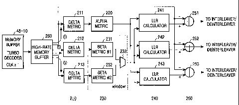
Referring to FIG. 8, the decoding apparatus according to an embodiment of the
present invention includes a SISO decoder comprised of a delta metric
calculation
section 210, an alpha metric calculation section 220, a beta metric
calculation section
230, an LLR calculation section 240, and a subtraction section 250. The
decoding
apparatus is characterized by further including a high-rate memory buffer 260
between
CA 02460315 2006-11-30
22
the SISO decoder and a memory buffer 46-10 that stores received symbols (or
data
bits) as described in FIG. 3. In addition, the memory buffer 46-10 of the
decoding
apparatus is featured by operating at a rate of { 1 xclock of turbo decoder}
rather than
at a rate of {3xclock of turbo deco(ter} of the memory buffer 46-1 in the
conventional
decoding apparatus (see FIGs. 7 and 11). That is, the proposed decoding
apparatus is
characterized by additionally arranging the high-rate memory buffer 260 after
the
memory buffer 46-10 to access received data bits stored in different positions
of the
memory buffer 46-10 for 1 clock of the turbo decoder and provide the accessed
data
bits to respective calculators 211 to 213 of the delta metric calculation
section 210 so
that a delta metric calculation operation by the delta metric calculation
section 210 is
performed for I clock of the turbo clecoder.
The proposed decoding apparatus, though used in a communication system
providing a high-speed packet data service such as a 1 x EV-DV system, is not
required to increase an operating frequency of the memory buffer. Thus, the
decoding
apparatus is suitable to enable a mobile communication terminal to consume
less
power. For reference, in the converitional decoding apparatus of FIG. 3, since
received
data bits are directly connected to the turbo decoder via the demultiplexer
205
connected to the memory buffer 46-1 of the receiver, a data reading operation
from the
memory buffer 46-1 of the receiver is performed three times as illustrated in
FIG. 6.
However, the decoding apparatus proposed in the invention is featured by
additionally
arranging the memory buffer 260 instead of the demultiplexer in an input stage
of the
decoder, thereby enabling a nonnal operation of the SISO decoder through one
reading operation for one clock. 'That is, the proposed decoding apparatus
requires
only one memory reading operation in calculating three delta metrics, and this
operation is identical to an operating clock of the turbo decoder. Such an
operation is
possible because the high-rate mernory buffer 260 previously stores a received
signal
therein and then rearranges the received signal to be matched with an input
desired by
the delta metric calculators 211 to 213.
Since the structure of the SISO decoder has been described before, a detailed
description thereof will be omitted, and a description of invention will now
be focused
on a structure and operation of the high-rate memory buffer 260 in relation to
the
CA 02460315 2006-11-30
23
invention.
The high-rate memory buffer 260 of the proposed decoding apparatus can be
constructed as illustrated in FIGs. 9, 12 and 17. FIG. 9 shows an embodiment
in which
the high-rate memory buffer 260 is comprised of one unidirectional shift
register 310
and as many bidirectional shift i-egisters 321, 322 and 323 as the number N of
windows. FIG. 12 shows an embocliment in which the high-rate memory buffer 260
is
comprised of one unidirectional shift register 410 and as many bidirectional
shift
registers 421 and 422 as the number 2 of windows. The structures shown in
FIGs. 9
and 12 are identical in principle, but different in the number of windows.
FIG. 17
shows an embodiment in which the high-rate memory buffer 260 is comprised of
one
bidirectional shift register 510 and as many bidirectional shift registers 521
and 522 as
the number 2 of windows. The structure shown in FIG. 17 is different in
principle
from the structures shown in FIGs. 9 and 12. In the structures shown in FIGs.
9 and
12, data bits from the memory buffer 46-10 are simultaneously applied to the
unidirectional shift register and the bidirectional shift registers. On the
contrary, in the
structure shown in FIG. 17, data bits from the memory buffer 46-10 are applied
to the
bidirectional shift registers 521 and 522, and data bits output from the
bidirectional
shift registers 521 and 522 are applied to the bidirectional shift register
510
corresponding to the unidirectional shift registers 310 and 410 in first and
second
embodiments.
The first, second and third embodiments of FIGS. 9, 12, and 17, respectively,
are disclosed in more detail below.
First Embodiment
FIG. 9 is a block diagram illustrating an example of a structure of the high-
rate
memory buffer 260 shown in FIG. 8 according to a first embodiment of the
present
invention. Referring to FIG. 9, the high-rate memory buffer 260 is comprised
of one
unidirectional shift register 310, N bidirectional shift registers 321 to 323,
a control
logic 330, dem.ultiplexers (DEMUX) 341 to 343, and multiplexers (MUX) 351 to
353.
The unidirectional shift register 310 has 2NW storage areas (length), and
includes an input terminal for data input and an output terminal for data
output. Here,
CA 02460315 2006-11-30
24
N is the number of windows and W is a size of the windows. The size W of the
windows can be changed. However, even though the size W of the windows is
changed, a ratio (e.g., 2W and 4W) of shift registers is not changed. For
W=24, the
unidirectional shift register 310 for a has a size of 96, and shift registers
321 to 323
for (31 and (32 have a size of 48. When W is changed, a length of the shift
registers is
changed accordingly, and a data processing flow will also be changed. However,
even
though W is changed, a structure of the shift registers is not changed. The
unidirectional shift register 310 sequentially receives input data bits from
the memory
buffer 46-10 through the input terminal according to a predetermined clock of
the
turbo decoder, and shifts the received input data bits from the left (side A)
to the right
(side B). When data bit streams of a first length (2NW) are formed, the
unidirectional
shift register 310 sequentially outputs the formed data bit streams of the
first length
through the output terminal. Data bits output from the unidirectional shift
register 310
are applied to the delta metric calculator 211 connected to a front end of the
alpha
metric calculation section 220.
The bidirectional shift registers 321 to 323 each have NW storage areas, and
include a first terminal and a second terminal for data input/output. The
first terminal
represents a terminal arranged in the left of each of the bidirectional shift
registers 321
to 323, while the second terminal represents a terminal arranged in the right
of each of
the bidirectional shift registers 321 to 323. The first terminal and the
second terminal
can support data output as well as data input. The number of the bidirectional
shift
registers 321 to 323 is determined by the number of windows. If the number of
windows is N, the number of the bidirectional shift registers 321 to 323 is
determined
as N, and if the number of windows is 2, the number of the bidirectional shift
registers
321 to 323 is determined as 2. Input data bits from the memory buffer 46-10
are
divided into groups each comprised of bits of a second length (NW) which is
1/2 of
the first length. The bidirectional shift registers 321 to 323 each
sequentially receive
and shift bits of odd-numbered groups among the divided groups through the
first
terminal from the left (side A) to the right (side B), and if bit streams of
the second
length are formed, the bidirectional shift registers 321 to 323 each
sequentially output
the formed bit streams through the first terminal from the right to the left,
which is the
reverse order of the input order. The bidirectional shift registers 321 to 323
each
CA 02460315 2006-11-30
sequentially receive and shift bits of even-numbered groups among the divided
groups
through the second terminal from the right to the left, and if bit streams of
the second
length are formed, the bidirectiona;l shift registers 321 to 323 each
sequentially output
the formed bit streams through the second terminal from the left to the right,
which is
5 the reverse order of the input order.
The demultiplexers 341 to :343 are provided between an output terminal of the
memory buffer 46-10 and the shift registers 321 to 323, and the multiplexers
351 to
353 are provided between the shift registers 321 to 323 and the delta metric
10 calculation section 210. Input terminals of the demultiplexers 341 to 343
are
connected to the output terminal of the memory buffer 46-10, first output
terminals of
the demultiplexers 341 to 343 are connected to second terminals of the shift
registers
321 to 323, and second output terminals of the demultiplexers 341 to 343 are
connected to first terminals of the shift registers 321 to 323. First input
terminals of
15 the multiplexers 351 to 353 are connected to second terminals of the shift
registers
321 to 323, second input terminals of the multiplexers 351 to 353 are
connected to
first terminals of the shift registers 321 to 323, and output terminals of the
multiplexers 351 to 353 are connected to the delta metric calculators 211 to
213.
20 The control logic 330 provides select signals selectl to selectN for
controlling
operations of the shift registers 321 to 323, the demultiplexers 341 to 343
and the
multiplexers 351 to 353. The select signals can be designated as signals for
controlling
input data bits from the memory buffer 46-10 so that the input data bits are
applied to
the shift registers 321 to 323 at different times. The control logic 330
determines
25 whether the input data bits from the memory buffer 46-10 are bits of odd-
numbered
groups or bits of even-numbered groups among the divided groups, and applies
the
input data bits from the memory buffer 46-10 to the first terminals or the
second
terminals of the shift registers 321 to 323 according to the determination
result.
For example, the control logic 330 outputs select signals of "0" or "logic
low"
level when the input data bits are bits of the odd-numbered groups, and the
control
logic 330 outputs select signals of "1" or "logic high" level when the input
data bits
are bits of the even-numbered groups. When select signals of "0" level are
output, the
CA 02460315 2006-11-30
26
demultiplexers 341 to 343 apply the input data bits from the memory buffer 46-
10 to
the first terminals of the shift registers 321 to 323. Then the shift
registers 321 to 323
sequentially shift the data bits received through their first terminals from
the left to the
right (in the right direction). At the same time, the shift registers 321 to
323
sequentially shift again NW data bits previously received through their second
terminals and then stored, from the left to the right, and output the shifted
data bits
through their second terminals.
When select signals of "1" level are output, the demultiplexers 341 to 343
apply the input data bits from the memory buffer 46-10 to the second terminals
of the
shift registers 321 to 323. Then the shift registers 321 to 323 sequentially
shift the data
bits received tllrough their seconcl terminals from the right to the left (in
the left
direction). At the same time, the shift registers 321 to 323 sequentially
shift again NW
data bits previously received through their first terminals and then stored,
from the
right to the left, and output the shifted data bits through their first
terminals.
Data bits output through the first terminals of the shift registers 321 to 323
are
applied to the second input terminals of the multiplexers 351 to 353, and data
bits
output through the second terminals of the shift registers 321 to 323 are
applied to the
first input tern7inals of the multiplexers 351 to 353. The multiplexers 351 to
353
multiplex data bits applied through their first input terminals and second
input
terminals, and output the multiplexed data bits to corresponding delta metric
calculators 211 to 213.
As described above, the proposed decoding apparatus applies data bits stored
in different positions of the memot-y buffer 46-10 to the SISO decoder using
the high-
rate memory buffer 260 having the structure illustrated in FIG. 9. That is,
the high-rate
memory buffer 260 rearranges the order of previously sequentially received
data bits
in the order requested by a SISO decoder with a sliding window mode scheme,
through the shift registers 310 and 321 to 323.
Referring to FIG. 9, M bits from the memory buffer 46-10 are applied to the
shift registers 310 and 321 to 323 having 2NW or NW storage areas. Here, N
indicates
CA 02460315 2006-11-30
27
the number of windows, W indicates a size of the windows, and M indicates the
number of data bits received from the memory buffer 46-10 for one clock of the
turbo
decoder. When the memory buffer 46-10 is a QCTC memory buffer, M is the sum of
a
bit width of systematic code and a bit width of parity codes. That is, an M-
bit signal is
a signal created by summing up M/3 bits of a systematic code, M/3 bits of a
first
parity code, and M/3 bits of a second parity code. For the M-bit signal input,
the shift
registers 310 and 321 to 323, the demultiplexers 341 to 343, and the
multiplexers 351
to 353 are all constructed to have an M-bit width. An output of the M-bit
signal, i.e.,
values output from the shift regisl:ers 310 and 321 to 323 are provided to the
delta
metric calculators 211 to 213. The delta metric calculators 211 to 213 receive
three
M/3-bit signals, the sum of which is M bits.
FIG. 10 illustrates a control operation by the control logic 330 shown in FIG.
9. Specifically, the drawing shows a control flow in which the control logic
330
controls the shift registers 321 to 323 for (3 metrics, the demultiplexers 341
to 343
connected to front ends and rear ends of the shift registers 321 to 323, and
the
multiplexers 351 to 353.
In FIG. 10, an operation in steps 1011 to 1017 represents a process flow of an
operation of controlling the shift register 321, the demultiplexer 341 and the
multiplexer 351. An operation in steps 1021 to 1027 represents a process flow
of an
operation of controlling the shift register 322, the demultiplexer 342 and the
multiplexer 352. An operation in steps 1031 to 1037 represents a process flow
of an
operation of controlling the shift register 323, the demultiplexer 343 and the
multiplexer 353. Since the respective process flows are identical in their
operations
except their start times and names of the signals used, only the process flow
in steps
1011 to 1017 will be described herein for simplicity. For such a control
operation,
counters corresponding to the shift registers 321 to 323 are included in the
control
logic 330. The counters are initialized at different times with a
predetermined offset of
W to perform a counting operationi. A counterl corresponding to the shift
register 321
is initialized at a time T=O, a counter2 corresponding to the shift register
322 is
initialized at a time T=Wt, and a counter #N corresponding to the shift
register 323 is
initialized at a time T=(N-1)Wt. Here, t represents a time, i.e., a unit
clock.
CA 02460315 2006-11-30
28
Referring to FIG. 10, in step 1011, the control logic 330 initializes the
shift
register 321. During the initialization operation, a count value of the
counterl is
initialized to countl=0, and a select signal selectl is initialized to
selectl=0. In
addition, a left (side A) terminal of the shift register 321 is designated as
an input
terminal, while a right (side B) terminal of the shift register 321 is
designated as an
output terminal. In step 1012, the control logic 330 reads data bits by
accessing the
memory buffer 46-10 of FIG. 8. In step 1013, the control logic 330 examines
whether
the count value is countl=NW in order to determine whether the shift register
321 is
full. If the count value is countl==NW, the control logic 330 sets the count
value
countl to 0 in step 1014. If the coiunt value is not countl=NW, the control
logic 330
increase the count value countl by 1 in step 1015. After the step 1014, the
control
logic 330 inverts the signal selectl in step 1016. That is, the control logic
330 converts
a signal selectl of "1" into a signal selectl of "0" and a signal selectl of
"0" into a
signal selectl of "1" by inverting the signal selectl. By the operation of
step 1016, an
input/output direction and a shift direction of data bits are changed. After
the step
1016 or after the step 1015, the control logic 330 writes data bits received
from the
memory buffer 46-10 in the shift i-egister 321, in step 1017. After the step
1017, the
control logic 330 returns to step 1012 to repeatedly perform the above
operation.
FIG. 11 is a timing diagram illustrating an example of a memory buffer access
operation timing perfonned by the high-rate memory buffer 260 shown in FIG. 9
according to an embodiment of the present invention. Referring to FIG. 11,
data bits
stored in different position of the memory buffer 46-10 are accessed by the
high-rate
memory buffer 260. In this example, the high-rate memory buffer 260 accesses
data
bits datal, data2 and data3 storeci in three addresses of the memory buffer 46-
10.
When the three kinds of data bits datal, data2 and data3 all enter the high-
rate
memory buffer 260 at the same time within one clock of the turbo decoder, the
calculators 211 to 213 of the delta metric calculation section 210 perform an
operation
of calculating a delta metric at the same time. The data bit datal (M bits)
refers to
systematic code (M/3 bits) + parityl code (M/3 bits) + parity2 code (M/3
bits), and the
data2 and data:3 are also equal to the datal.
Second Embodiment
CA 02460315 2006-11-30
29
FIG. 12 is a block diagram illustrating another example of a structure of the
high-rate memory buffer 260 shown in FIG. 8 according to a second embodiment
of
the present invention. The drawing shows a structure of the high-rate memory
buffer
260 when the number of windows is N=2, i.e., when beta has two windows.
Referring to FIG. 12, the Iiigh-rate memory buffer 260 is comprised of one
unidirectional shift register 410, N=2 bidirectional shift registers 421 and
422, a
control logic 430, demultiplexers (DEMUX) 441 and 442, and multiplexers (MUX)
451 and 452.
The shift register 410 has 2NW=4W storage areas (length), and includes an
input terminal for data input and an output terminal for data output. The
shift register
410 sequentially receives input data bits from the memory buffer 46-10 through
the
input terminal according to a clock: of the turbo decoder, and shifts the
received input
data bits from the left (side A) to the right (side B). When data bit streams
of a first
length (4W) are formed, the shift register 410 sequentially outputs the formed
data bit
streams of the first length through the output terminal. Data bits output from
the shift
register 410 are applied to the delta metric calculator 211 connected to a
front end of
the alpha metric calculation section 220.
The shift registers 421 and 422 each have NW=2W storage areas, and include
a first terminal and a second terminal for data input/output. The first
terminal
represents a terminal arranged in the left of each of the shift registers 421
and 422,
while the second terminal represents a terminal arranged in the right of each
of the
shift registers 421 and 422. The first terminal and the second terminal can
support data
output as well as data input. The number of the shift registers 421 and 422 is
determined by the number of windows. If the number of windows is N=2, the
number
of the shift registers 421 and 422 is determined as 2. Input data bits from
the memory
buffer 46-10 are divided into groups each comprised of bits of a second length
(2W)
which is 1/2 of the first length. The shift registers 421 and 422 each
sequentially
receive and shift bits of odd-numbered groups among the divided groups through
the
first terminal from the left (side A) to the right (side B), and if bit
streams of the
second length are formed, the shift registers 421 and 422 each sequentially
output the
CA 02460315 2006-11-30
formed bit streams through the first terminal from the right to the left, the
reverse
order of the input order. The shift registers 421 and 422 each sequentially
receive and
shift bits of even-numbered groups among the divided groups through the second
terminal from the right to the left, and if bit streams of the second length
are formed,
5 the shift registers 421 and 422 each sequentially output the formed bit
streams through
the second terminal from the left to the right, the reverse order of the input
order.
The demultiplexers 441 and 442 are provided between an output terminal of
the memory buffer 46-10 and the shift registers 421 and 422. The multiplexers
451
10 and 452 are provided between the shift registers 421 and 422 and the delta
metric
calculation section 210. Input terminals of the demultiplexers 441 and 442 are
connected to the output terminal of the memory buffer 46-10, first output
terminals of
the demultiplexers 441 and 442 are connected to second terminals of the shift
registers
421 and 422, and second output terminals of the demultiplexers 441 and 442 are
15 connected to first terminals of the shift registers 421 and 422. First
input terminals of
the multiplexers 451 and 452 are connected to second terminals of the shift
registers
421 and 422, second input terminals of the multiplexers 451 and 452 are
connected to
first terminals of the shift registers 421 and 422, and output terminals of
the
multiplexers 451 and 452 are connected to the delta metric calculators 211 to
213.
The control logic 430 provides select signals selectl and select2 for
controlling
operations of the shift registers 421 and 422, the demultiplexers 441 and 442,
and the
multiplexers 451 and 452. The select signals can be designated as signals for
controlling input data bits from the memory buffer 46-10 so that the input
data bits are
applied to the shift registers 421 and 422 at different times. The control
logic 430
determines whether the input data bits from the memory buffer 46-10 are bits
of odd-
numbered groups or bits of even-numbered groups among the divided groups, and
applies the input data bits from the memory buffer 46-10 to the first
terminals or the
second terminals of the shift registers 421 and 422 according to the
determination
result.
For example, the control logic 430 outputs select signals of "0" or "logic
low"
level when the input data bits are bits of the odd-numbered groups, and the
control
CA 02460315 2006-11-30
31
logic 430 outputs select signals of "1" or "logic high" level when the input
data bits
are bits of the even-numbered groups. When select signals of "0" level are
output, the
demultiplexers 441 and 442 apply the input data bits from the memory buffer 46-
10 to
the first terminals of the shift registers 421 and 422. Then the shift
registers 421 and
422 sequentially shift the data bits received through their first terminals
from the left
to the right (in the right direction). At the same time, the shift registers
421 and 422
sequentially shift again 2W data bits previously received through their second
terminals and then stored, from the left to the right, and output the shifted
data bits
through their second terminals.
When select signals of "1" level are output, the demultiplexers 441 and 442
apply the input data bits from the rnemory buffer 46-10 to the second
terminals of the
shift registers 421 and 422. Then t:he shift registers 421 and 422
sequentially shift the
data bits received through their second terminals from the right to the left
(in the left
direction). At the saine time, the shift registers 421 and 422 sequentially
shift again
2W data bits previously received trirough their first terminals and then
stored, from the
right to the left, and output the shifted data bits through their first
terminals.
Data bits output through the first terminals of the shift registers 421 and
422
are applied to the second input terminals of the multiplexers 451 and 452, and
data
bits output through the second ternninals of the shift registers 421 and 422
are applied
to the first input terminals of the multiplexers 451 and 452. The multiplexers
451 and
452 multiplex data bits applied through their first input terminals and second
input
terminals, and output the multiplexed data bits to corresponding delta metric
calculators 211 to 213.
Referring to FIG. 8, the calculators 211 to 213 of the first metric
calculation
section 210 receive output bits of the shift registers 410, 421 and 422, and
calculate
corresponding delta metrics. The second metric calculation section 220
calculates an
alpha metric by receiving a delta metric from the calculator 211 of the first
metric
calculation section 210, corresponding to the shift register 410. The third
metric
calculation section 230 calculates beta metrics by receiving delta metrics
from the
calculators 212 and 213 of the first metric calculation section 210,
corresponding to
CA 02460315 2006-11-30
32
the shift registers 421 and 422. 'The calculators 241 to 243 of the fourth
metric
calculation section 240 calculate LLR values corresponding to the shift
registers 410,
421 and 422 by receiving the alpha metric and a multiplexing result of the
beta
metrics by the multiplexer 233. The subtracters 251 to 253 of the subtraction
section
250 subtract an output of the shift register 410 from the respective LLR
values, and
output the subtraction results for interleaving and deinterleaving.
FIG. 13 is a flow chart illustrating an example of a control operation
performed by the control logic 430 shown in FIG. 12 according to an embodiment
of
the present invention. Specifically, the drawing shows a control flow in which
the
control logic 430 controls the bidirectional shift registers 421 and 422 for
(3 metrics,
the demultiplexers 441 and 442 connected to front ends and rear ends of the
shift
registers 421 and 422, and the multiplexers 451 and 452.
In FIG. 13, asl operation in steps 111 I to 1117 represents a process flow of
an
operation of controlling the shift register 421, the demultiplexer 441 and the
multiplexer 451. An operation in steps 1121 to 1127 represents a process flow
of an
operation of controlling the shift register 422, the demultiplexer 442 and the
multiplexer 452. Since the respective process flows are identical in their
operations
except their start times and names of the signals used, only the process flow
in steps
1111 to 1117 will be described herein for simplicity. For such a control
operation,
counters corresponding to the shift registers 421 and 422 are included in the
control
logic 430. The counters are initialized at different times with a
predetermined offset of
W to perform a counting operation. A counterl corresponding to the shift
register 421
is initialized at a time T=O, and a counter2 corresponding to the shift
register 422 is
initialized at a time T=Wt. Here, t represents a time, i.e., a unit clock.
Referring to FIG. 13, in step 1111, the control logic 430 initializes the
shift
register 421. During the initialization operation, a count value of the
counterl is
initialized to countl=0, and a select signal selectl is initialized to
selectl=0. In
addition, a left (side A) terminal of the shift register 421 is designated as
an input
terminal, while a right (side B) terminal of the shift register 421 is
designated as an
output terminal. In step 1112, the control logic 430 reads data bits by
accessing the
CA 02460315 2006-11-30
33
memory buffer 46-10 of FIG. 8. In step 1113, the control logic 430 examines
whether
the count value is countl=2W in order to determine whether the shift register
421 is
full. If the count value is countl=2W, the control logic 430 sets the count
value countl
to 0 in step 1114. If the count value is not countl=2W, the control logic 430
increase
the count value countl by 1 in step 1115. After the step 1114, the control
logic 430
inverts the signal selectl in step 1116. That is, the control logic 430
converts a signal
selectl of "I" into a signal selectl of "0" and a signal selectl of "0" into a
signal
selectl of "1" by inverting the signal selectl. By the operation of step 1116,
an
input/output direction and a shift direction of data bits are changed. After
the step
1116 or after the step 1115, the control logic 430 writes data bits received
from the
memory buffer 46-10 in the shift register 421, in step 1117. After the step
1117, the
control logic 430 returns to step 1112 to repeatedly perform the above
operation.
FIG. 14 is-a block diagram illustrating an example of a data processing flow
performed by the shift register 410 for an alpha metric, shown in FIG. 12.
Referring to
FIG. 14, the shift register 410 sequentially receives and shifts data bits
from the
memory buffer 46-10 of FIG. 8 from the lefl to the right. In the drawing,
"side A" a
position where data bits are input, and "side B" represents a position where
data bits
are output. When data bits are input to the shift register 410, the input data
bits are
output after being delayed by 4W. The shift register 410 simply has a (FIFO)
First-In
First-Out structure.
FIG. 15 illustrates a data processing flow by the shift register 421 for a
beta
metric, shown in FIG. 12. This data processing flow is identical to a data
processing
flow for the other shift register 422 for a beta metric.
Referring to FIG. 15, the shift register 421 delays data sequentially read
from
the memory buffer 46-10 for a predetermined time in order to match a data
output
time to a time desired by the turbo decoder. The shift register 421
sequentially stores
input data bits. If the shift register 421 is full, the shift register 421
outputs previous
data bits while shifting the stored data bits in the opposite direction of an
input
direction, and the output data bits are provided to the delta metric
calculator 212. As a
result, an empty space occurs in the opposite side of the shift register 421.
Such an
CA 02460315 2006-11-30
34
empty space is filled again as new data bits are input in the opposite
direction of an
input direction in which the previous data bits were input. In this way, data
input and
output operations of the shift register 421 are repeated, and as a result,
data bits are
provided to the corresponding delta metric calculator 212 according to the
data flow
illustrated in the drawing.
FIG. 16 is a block diagram illustrating an example of a memory buffer access
operation timing performed by the high-rate memory buffer 260 shown in FIG. 12
according to an embodiment of the present invention. In FIG. 16, "delta block
input
for alpha" represents input/output data bits of the unidirectional shift
register 410 of
FIG. 12, wherein "side A in" indicates input data bits while "side B out"
indicates
output data bits. In addition, "delta block input for beta 1" represents
input/output data
bits of the bidirectional shift register 421, and "delta block input for
beta2" represents
input/output data bits of the bidirectional shift register 422. In "delta
block input for
betal" and "delta block input for beta2," "side A in" and "side A out"
indicate data
bits being input/output through the first terminal, while "side B in" and
"side B out"
indicate data bits being input/output through the second terminal. "selectl"
and
"select2" represent control signals which were generated by the control logic
430 and
then provided to the shift registers 421 and 422. "a out," "(31 out" and "(32
out"
represent finally output metrics, aind an LLR value is calculated using such
output
metrics.
In the "delta block input for betal" part, data bits are input through side A
at
the initial stage. The data bits are input in order of a, b, c, d, ===, h, and
the data bits are
output at side A after a lapse of 2W from an initial period. While an output
operation
is performed at side A, an input operation is performed through side B. This
means
that the shift register 421 is operating by changing its shift direction.
After a lapse of
another 2W, when an input operation is performed again at side A and then a
q"' data
bit is input, a pth data bit is output at side B.
An operation in a "delta block input for beta2" part is performed in the same
manner as the operation in the "delta block input for betal" part. However,
since an
initialization time of the shift register 422 is different from an
initialization time of the
CA 02460315 2006-11-30
shift register 421, input/output of the data bits is not performed in the same
period.
In "delta block input for alpha," only input operation is performed at side A,
and only output operation is performed at side B. A first received a"' data
bit is output
5 at a time when 4W has elapsed from an initial period.
Comparing the output data bits of the shift registers 410, 421 and 422 with
the
output data bits shown in FIG. 6, :it can be understood that the data bits are
output in
the same flow. However, there is a difference in that an output method of FIG.
16
10 generates an initial delay of 2W compared with an output method of FIG. 6.
Such a
difference, however, occurs while the high-rate memory buffer 260 is initially
operated. That is, since the difference occurs only at an initial stage when
decoding of
the turbo decoder is started, it does not affect decoding performance.
15 Third Embodiment
FIG. 17 is a block diagram illustrating another example of the high-rate
memory buffer 260 shown in FIG. 8 according to a third embodiment of the
present
invention. Referring to FIG. 17, the high-rate memory buffer 260 is comprised
of first
stage's bidirectional shift registers 521 and 522, a second stage's
bidirectional shift
20 register 510, a control logic 530, demultiplexers 541 and 542, and
multiplexers 551 to
553.
The first stage's bidirectional shift registers 521 and 522 each have NW
storage areas (length), and include a first terminal and a second terminal for
data
25 input/output. Here, N indicates the number of windows, and W indicates a
size of the
windows. The number of the shift registers is determined by the number of
windows,
and the number of storage areas is determined by multiplying the number of the
windows by the size of the windows. The first terminal represents a terminal,
i.e., a
terminal of side A, arranged in the left of each of the shift registers 521
and 522, while
30 the second terminal represents a terminal, i.e., a terminal of side B,
arranged in the
right of each of the shift register-s 521 and 522. The first terminal and the
second
terminal can support data outpult as well as data input. Input data bits from
the
memory buffer 46-10 are dividecl into groups each comprised of bits of the
length
CA 02460315 2006-11-30
36
NW. The shift registers 521 and 522 each sequentially receive and shift bits
of odd-
numbered groups among the divided groups through the first terminal from the
left
(side A) to the right (side B), and if bit streams of the length are formed,
the shift
registers 521 and 522 each sequentially output the formed bit streams through
the first
terminal from the right to the left, the reverse order of the input order. The
shift
registers 521 and 522 each sequentially receive and shift bits of even-
numbered
groups among the divided groups through the second terminal from the right
(side B)
to the left (side A), and if bit streams of the length are formed, the shift
registers 521
and 522 each sequentially output the formed bit streams through the second
terminal
from the left to the right, the reverse order of the input order.
The second stage's bidirectional shift register 510 has NW storage areas, and
includes a third terminal and a fourth terminal for data input/output. The
shift register
510 receives bits sequentially output via the first terminal of the shift
register 521, via
its third terminal, and sequentially shifts the received bits from the left to
the right. If
bit streams of the length are formed, the shift register 510 shifts the formed
bit streams
from the right to the left, the reverse order of the input order, and
sequentially outputs
the shifted bit streams via the third terminal. The shift register 510
receives bits
sequentially output via the second terminal of the shift register 521, via its
fourth
terminal, and sequentially shifts ithe received bits from the right to the
left. If bit
streams of the lengtll are formed, the shift register 510 shifts the forrned
bit streams
from the left to the right, the reverse order of the input order, and
sequentially outputs
the shifted bit streams via the fourth terminal.
The demultiplexers 541 and 542 are provided between an output terminal of
the memory buffer 46-10 and the shift registers 521 and 522, and the
multiplexers 551
to 553 are provided between the shift registers 510, 521 and 522 and the delta
metric
calculation section 210. Input terminals of the demultiplexers 541 and 542 are
connected to the output terminal of the memory buffer 46-10, first output
terminals of
the demultiplexers 541 and 542 are connected to second terminals of the shift
registers
521 and 522, and second output terininals of the demultiplexers 541 and 542
are
connected to first terminals of the shift registers 521 and 522. First input
terminals of
the multiplexers 551 to 553 are connected to second terminals of the shift
registers
CA 02460315 2006-11-30
37
510, 521 and 522, second input terrninals of the multiplexers 551 to 553 are
connected
to first terminals of the shift registers 510, 521 and 522, and output
terminals of the
multiplexers 551 to 553 are connected to the delta metric calculators 211 to
213.
The control logic 530 provides select signals selectl, select2 and select3 for
controlling operations of the shift registers 510, 521 and 522, the
demultiplexers 541
and 542, and the multiplexers 551 to 553. The select signals can be designated
as
signals for controlling input data bits from the memory buffer 46-10 so that
the input
data bits are applied to the shift registers 521 and 522 at different times.
The control
logic 530 determines whether the input data bits from the memory buffer 46-10
are
bits of odd-numbered groups or bits of even-numbered groups among the divided
groups, and provides the shift registers 521 and 522 with select signals
select2 and
select3 for applying the input data bits to the first terminals or the second
terminals
according to the determination result.
For example, the control logic 530 outputs select signals of "0" or "logic
low"
level when the input data bits are bits of the odd-numbered groups, and the
control
logic 330 outputs select signals of' "1" or "logic high" level when the input
data bits
are bits of the even-numbered groups. When select signals of "0" level are
output, the
demultiplexers 541 and 542 apply the input data bits from the memory buffer 46-
10 to
the first terminals of the shift registers 521 and 522. Then the shift
registers 521 and
522 sequentially shift the data bits received through their first terminals
from the left
to the right (in the right direction). At the same time, the shift registers
521 and 522
sequentially shift again 2W data bits previously received through their second
terminals and then stored, from the left to the right, and output the shifted
data bits
through their second terminals.
When select signals of "1" level are output, the demultiplexers 541 and 542
apply the input data bits from the memory buffer 46-10 to the second terminals
of the
shift registers 521 and 522. Then the shift registers 521 and 522 sequentially
shift the
data bits received through their second terminals from the right to the left
(in the left
direction). At the same time, the shift registers 521 and 522 sequentially
shift again
2W data bits previously received tlirough their first terminals and then
stored, from the
CA 02460315 2006-11-30
38
right to the left, and output the shifted data bits through their first
terminals.
Data bits output through the first terminals of the shift registers 521 and
522
are applied to the second input terminals of the multiplexers 552 and 553, and
data
bits output through the second terminals of the shift registers 521 and 522
are applied
to the first input terminals of the multiplexers 552 and 553. The multiplexers
552 and
553 multiplex data bits applied through their first input terminals and second
input
terminals, and output the multiplexed data bits to corresponding delta metric
calculators 211 to 213.
Data bits output via the first terminal of the shift register 521 are also
applied
to the first terminal of the shift register 510, and data bits output via the
second
terminal of the shift register 521 are also applied to the second terminal of
the shift
register 510. An operation of the shift register 510 is equal to the
operations of the
shift registers 521 and 522. Data bits output via the first terminal of the
shift register
510 are applied to the second input terminal of the multiplexer 551, and data
bits
output via the second terminal of the shift register 510 are applied to the
first input
terminal of the multiplexer 551. Data bits output from the multiplexer 551 are
applied
to the delta metric calculator 211 connected to a front end of the alpha
metric
calculator 220.
This embodiment of the present invention is different in structure from the
high-rate memory buffer 260 shown in FIG. 12, but identical in terms of
operation.
According to this embodiment of the present invention, the shift register 510
for an a
metric is a bidirectional shift register having a length of 2W unlike the
embodiments
shown in FIGs. 9 and 12, and the shift register 510 receives the data bits
provided
from the shift register 521 for a(3 1 metric, instead of receiving the data
bits provided
from the memory buffer 46-10, and then outputs the data bits via the
multiplexer 551.
That is, the shift register 510 with the same structure receives again the
output of the
shift register 521 for a R 1 metric. In this embodiment, if the shift register
521 for a(31
metric is arranged in the reverse order of an actually received signal, it is
reconstructed in the reverse order to restore a signal in order of an original
input signal
and then apply the restored signal to the shift register 510 for an a metric.
If the high-
CA 02460315 2006-11-30
39
rate memory buffer is constructed so that the shift register 510 for an a
metric and the
sift register 521 for a(31 metric always operate in the opposite direction,
the memory
buffer can reduce a size of the shift registers by 2W, compared to the high-
rate
memory buffer shown in FIG. 12.
FIG. 18 is a flow chart illustrating an example of a control operation
performed by the control logic 530 of FIG. 17 according to an embodiment of
the
present invention. A process flow for the control operation shown in the
drawing is
similar to the process flow illustrated in FIG. 13. However, the only
difference is that
a flow for controlling the shift register 510 for an a metric is added. In the
control
flow, steps 1211, 1221 and 1231 indicating initialization processes are
different.
Referring to FIG. 18, the shift register 510 for an a metric is initialized at
a
time T=(2W-1)t, and the shift register 521 for a(31 metric is initialized at a
time T=O,
and the shift register 522 for a(32 metric is initialized at a time T=(W-1)t.
That is, the
shift register 510 is initialized after a clock (2W-1), the shift register 521
is initialized
at a clock 0, and the shift register 522 is initialized after a clock (W-1).
Considering
that the entire period of the shift registers is 4W, it is noted that the two
shift registers
operate in the opposite direction at periods of 2W. Except for the
initialization
processes, FIG. 18 is identical in operation to FIG. 13, so a detailed
description
thereof will be omitted for simplicity.
FIG. 19 is a block diagram illustrating an example of a data processing flow
performed by the shift register 510 of FIG. 17 according to an embodiment of
the
present invention. Referring to FIG. 19, the data processing operation by the
shift
register 510 is performed in the same way as the data processing operation by
the shift
registers for a(3 metric, described in conjunction with FIG. 15.
FIG. 20 is a block diagrarn illustrating an example of a memory buffer access
operation timing performed by the high-rate memory buffer 260 of FIG. 17
according
to an embodiment of the present invention. Referring to FIG. 20, a memory
buffer
access operation by the high-rate memory buffer 260 is different in operation
of the
CA 02460315 2006-11-30
shift register 510, but provides the same a, (31 and (32 metrics in
conclusion.
As described above, the invention provides data bits from a memory buffer of
a receiver to a turbo decoder by using a high-rate memory buffer having the
same
5 operating frequency as the turbo decoder. In addition, the invention enables
realization
of an apparatus suitable for a mobile communication environment requiring
lower
power consumption, by removing a necessity to increase an operating frequency
of a
memory buffer of a receiver.
10 While the invention has been shown and described with reference to a
certain
embodiments thereof, it will be understood by those skilled in the art that
various
changes in form and details may be made therein without departing from the
spirit and
scope of the invention as defined by the appended claims and equivalents
thereof.