Note : Les descriptions sont présentées dans la langue officielle dans laquelle elles ont été soumises.
CA 02462429 2004-03-31
WO 03/030219 PCT/US02/31710
HIGH PRESSURE PROCESSING CHAMBER FOR
MULTIPLE SEMICONDUCTOR SUBSTRATES
FIELD OF THE INVENTION
This invention relates to the field of high pressure processing chambers for
semiconductor substrates. More particularly, this invention relates to the
field of high
pressure processing chambers for semiconductor substrates where a high
pressure processing
chamber provides processing capability for simultaneous processing of multiple
semiconductor substrates.
BACKGROUND OF THE INVENTION
Recently, interest has developed in supercritical processing for semiconductor
substrates for such processes as photoresist removal, rinse agent drying, and
photoresist
development. The supercritical processing is a high pressure processing where
pressure and
temperature are at or above a critical pressure and a critical temperature.
Above the critical
temperature and the critical pressure, there is no liquid or gas phase.
Instead, there is a
supercritical phase.
A typical semiconductor substrate is a semiconductor wafer. The semiconductor
wafer has a thin cross-section and a~ large diameter. Currently, semiconductor
wafers have
diameters up to 300 mm. Because of a capital outlay for both semiconductor
development
and for semiconductor processing equipment, semiconductor processing must be
efficient,
reliable, and economical.
Thus, a supercritical processing system intended for semiconductor processing
of
multiple semiconductor substrates must have a high pressure processing chamber
which is
efficient, reliable, and economical.
What is needed is a high pressure processing chamber for processing multiple
semiconductor substrates which is efficient, reliable, and economical.
SUMMARY OF THE INVENTION
The present invention is a high pressure processing chamber for processing
multiple
semiconductor substrates. The high pressure processing chamber comprises a
chamber
housing, a cassette, and a chamber closure. The cassette is removably coupled
to the
chamber housing. The cassette is conftgured to accommodate at least two
semiconductor
substrates. The chamber closure is coupled to the chamber housing. The chamber
closure is
configured such that in operation the chamber closure seals with the chamber
housing to
provide an enclosure for high pressure processing of the semiconductor
substrates.
BRIEF DESCRIPTION OF THE DRAWINGS
FIG. 1 illustrates the preferred high pressure processing chamber and a
lifting
mechanism of the present invention.
CA 02462429 2004-03-31
WO 03/030219 PCT/US02/31710
FIGS. 2A and 2B illustrate a locking ring of the present invention.
FIG. 3 further illustrates the preferred high pressure processing chamber of
the
present invention.
FIG. 4 illustrates the preferred cassette of the present invention.
FIGS. SA and SB illustrate a chamber housing, first and second cassettes, and
a robot
of the present invention.
FIGS. 6A and 6B illustrate an injection nozzle arrangement and a fluid outlet
arrangement of the present invention.
FIG. 7 illustrates a supercritical processing system of the present invention.
FIG. 8 illustrates a first alternative high pressure processing chamber of the
present
invention.
FIG. 9 illustrates a first alternative cassette of the present invention.
FIG. 10 illustrates a second alternative cassette of the present invention.
DETAILED DESCRIPTION OF THE PREFERRED EMBODIMENT
Preferably, the preferred high pressure processing chamber of the present
invention
simultaneously processes multiple semiconductor substrates. Preferably, the
semiconductor
substrates comprise semiconductor wafers. Alternatively, the semiconductor
substrates
comprise other semiconductor substrates such as semiconductor pucks. Further
alternatively,
the semiconductor substrates comprise trays with each tray capable of holding
multiple
semiconductor devices.
Preferably, the preferred high pressure processing chamber of the present
invention
provides a supercritical processing environment. More preferably, the
preferred high
pressure processing chamber provides a supercritical COZ processing
environment.
Preferably, the supercritical COZ processing environment comprises a drying
environment for
drying developed photoresist which has been rinsed but not dried.
Alternatively, the
supercritical COZ processing environment comprises an alternative drying
environment for
other semiconductor drying processes such as drying MEMS devices.
Alternatively, the
supercritical COz processing environment comprises a photoresist development
environment.
Further alternatively, the supercritical COZ processing environment comprises
a
semiconductor cleaning environment, for example, for a photoresist and residue
cleaning or
for a CMP (chemical mechanical planarization) residue cleaning.
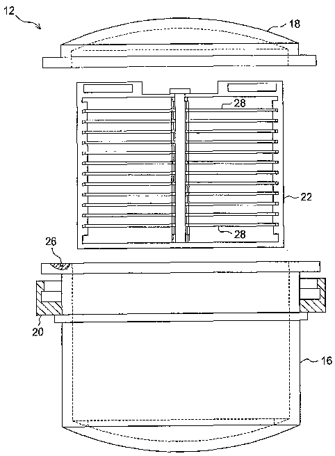
A high pressure processing chamber assembly of the present invention is
illustrated in
FIG. 1. The high pressure processing chamber assembly 10 comprises the
preferred high
pressure processing chamber 12 and a lid lifting mechanism 14. The preferred
high pressure
processing chamber 12 comprises a chamber housing 16, a chamber lid 18, a
locking ring 20,
a preferred cassette 22, and a first o-ring seal 26. Preferably, the chamber
housing 16 and the
chamber lid 18 comprise stainless steel. Preferably, the locking ring 20
comprises high
tensile strength steel. Preferably, the preferred cassette 22 comprises
stainless steel.
CA 02462429 2004-03-31
WO 03/030219 PCT/US02/31710
Alternatively, the preferred cassette 22 comprises a corrosion resistant
metal. Further
alternatively, the preferred cassette 22 comprises a corrosion resistant
polymer material.
The lid lifting mechanism 14 couples to the chamber lid 18. The locking ring
20
couples to the chamber housing 16. When the preferred high pressure processing
chamber 12
is closed, the locking ring 20 couples the chamber housing 16 to the chamber
lid 18 to form a
processing enclosure 24. The preferred cassette 22 couples to an interior of
the chamber
housing 16.
In use, the locking ring 20 locks the chamber lid 18 to the chamber housing
16. The
locking ring 20 also maintains a sealing force between the chamber lid 18 and
the chamber
housing 16 to preclude high pressure fluid within the processing enclosure 24
from leaking
past the first o-ring seal 26. When the locking ring 20 is disengaged from the
chamber lid 18,
the lid lifting mechanism 14 raises the lid 18 and swings the lid 18 away from
the chamber
housing 16.
The locking ring 20 of the present invention is further illustrated in FIGS.
2A and 2B.
The locking ring 20 comprises a broken thread and a lip 21. The broken thread
comprises
mating surfaces 23, which mate to corresponding features on the chamber
housing 16 (FIG.
1).
The high pressure processing chamber 10 is further illustrated in FIG. 3. In
operation,
the preferred cassette 22 preferably holds semiconductor wafers 28. A robot
(not shown)
preferably loads the preferred cassette 22 into the chamber housing 16 and
retracts. The lid
lifting mechanism 14 (FIG. 1) then lowers the chamber lid 18 onto the chamber
housing 16.
Following this, the locking ring 20 locks and seals the chamber lid 18 to the
chamber housing
16. Subsequently, the semiconductor wafers are preferably processed in the
supercritical
environment. Next, the lid lifting mechanism 14 raises the chamber lid 18.
Finally, the robot
removes the preferred cassette 22 from the chamber housing 16.
The preferred cassette 22 of the present invention is further illustrated in
FIG. 4. The
preferred cassette 22 comprises a cassette frame 30 and a retaining bar 32.
The cassette
frame 30 comprises wafer holding slots 34, and lifting features 36.
Preferably, the retaining
bar 32 is coupled to the cassette frame 30 via a hinge 38. Preferably, in use,
the
semiconductor wafers 28 (one shown with dashes lines) are loaded into the
preferred cassette
22. More preferably, the semiconductor wafers are loaded into the preferred
cassette 22 by a
transfer of the semiconductor wafers 28 from a FOUP (front opening unified
pod) to
preferred cassette 22. Once the semiconductor wafers 28 are loaded into the
preferred
cassette 22, the retaining bar 32 is preferably snapped into a retaining slot
40 in the cassette
frame 3 0.
An automated processing arrangement of the present invention is illustrated in
FIGS.
SA and SB. The automated processing arrangement 41 comprises the chamber
housing 16,
the robot 42, and first and second cassettes, 44 and 46. The robot 42
comprises a robot base
48, a vertical motion unit 49, a robot arm 50, and a forked cassette interface
52. The robot
base 48 provides a rotation movement A for the robot arm 50. The vertical
motion unit 49
CA 02462429 2004-03-31
WO 03/030219 PCT/US02/31710
provides a vertical movement B for the robot arm 50. Prior to processing, the
first and
second cassettes, 44 and 46, are loaded with the semiconductor wafers 28. In
operation, the
robot arm 50 extends the forked cassette interface 52 through the lifting
features 36 of the
first cassette 44, lifts the first cassette 44, moves the first cassette 44 to
a position above the
chamber housing 16, lowers the first cassette into the chamber housing 16, and
retracts the
forked cassette interface 52. Following this, the semiconductor wafers 28 in
the first cassette
44 are processed. Next, the robot 42 extends the forked cassette interface 52
through the
lifting features 36 of the first cassette 44 and removes the first cassette 44
from the chamber
housing 16. Subsequently, the robot 42 handles the second cassette 46 holding
more of the
semiconductor wafers 28 in a similar fashion to the handling of the first
cassette 44.
An injection nozzle arrangement and a fluid outlet arrangement of the present
invention is illustrated in FIGS. 6A and 6B. Preferably, the injection nozzle
arrangement 54
and fluid outlet arrangement 56 are located within the chamber housing 16.
Alternatively,
the injection nozzle arrangement 54 forms part of the preferred cassette 22
(FIG. 4). Further
alternatively, the fluid outlet arrangement 56 forms part of the preferred
cassette 22 (FIG. 4).
The injection nozzle arrangement 54 comprises a reservoir 58 and injection
nozzles 60. The
fluid outlet arrangement 56 comprises fluid outlets 62 and a drain 64. In
operation, the
injection nozzle arrangement 54 and the fluid outlet arrangement 56 work in
conjunction to
provide a processing fluid flow 66 across the semiconductor wafers 28.
A supercritical processing system of the present invention is illustrated in
FIG. 7.
The supercritical processing system 200 includes the preferred high pressure
processing
chamber 12, a pressure chamber heater 204, a carbon dioxide supply arrangement
206, a
circulation loop 208, a circulation pump 210, a chemical agent and rinse agent
supply
arrangement 212, a separating vessel 214, a liquid/solid waste collection
vessel 217, and a
liquefying/purifying arrangement 219. The carbon dioxide supply arrangement
206 includes
a carbon dioxide supply vessel 216, a carbon dioxide pump 218, and a carbon
dioxide heater
220. The chemical agent and rinse agent supply arrangement 212 includes a
chemical supply
vessel 222, a rinse agent supply vessel 224, and first and second high
pressure injection
pumps, 226 and 228.
The carbon dioxide supply vessel 216 is coupled to the high pressure
processing
chamber 12 via the carbon dioxide pump 218 and carbon dioxide piping 230. The
carbon
dioxide piping 230 includes the carbon dioxide heater 220 located between the
carbon
dioxide pump 218 and the high pressure processing chamber 12. The pressure
chamber
heater 204 is coupled to the high pressure processing chamber 12. The
circulation pump 210
is located on the circulation loop 208. The circulation loop 208 couples to
the high pressure
processing chamber 12 at a circulation inlet 232 and at a circulation outlet
234. The chemical
supply vessel 222 is coupled to the circulation loop 208 via a chemical supply
line 236. The
rinse agent supply vessel 224 is coupled to the circulation loop 208 via a
rinse agent supply
line 238. The separating vessel 214 is coupled to the high pressure processing
chamber 12
CA 02462429 2004-03-31
WO 03/030219 PCT/US02/31710
via exhaust gas piping 240. The liquid/solid waste collection vessel 217 is
coupled to the
separating vessel 214.
The separating vessel 214 is preferably coupled to the liquefying/purifying
arrangement 219 via return gas piping 241. The liquefying/purifying
arrangement 219 is
preferably coupled to the carbon dioxide supply vessel 216 via liquid carbon
dioxide piping
243. Alternatively, an off site location houses the liquefying/purifying
arrangement 219,
which receives exhaust gas in gas collection vessels and returns liquid carbon
dioxide in
liquid carbon dioxide vessels.
The pressure chamber heater 204 heats the high pressure processing chamber 12.
Preferably, the pressure chamber heater 204 is a heating blanket.
Alternatively, the pressure
chamber heater is some other type of heater.
Preferably, first and second filters, 221 and 223, are coupled to the
circulation loop
208. Preferably, the first filter 221 comprises a fme filter. More preferably,
the first filter
221 comprises the fine filter configured to filter 0.05 ~,m and larger
particles. Preferably, the
second filter 223 comprises a coarse filter. More preferably, the second
filter 223 comprises
the coarse filter configured to filter 2-3 ~,m and larger particles.
Preferably, a third filter 225
couples the carbon dioxide supply vessel 216 to the carbon dioxide pump 218.
Preferably,
the third filter 225 comprises the fme filter. More preferably, the third
filter 225 comprises
the fme filter configured to filter the 0.05 ~,m and larger particles.
It will be readily apparent to one skilled in the art that the supercritical
processing
system 200 includes valuing, control electronics, and utility hookups which
are typical of
supercritical fluid processing systems.
A first alternative high pressure processing chamber of the present invention
is
illustrated in FIG. 8. The first alternative high pressure processing chamber
12A comprises
an alternative chamber housing 16A, an alternative chamber lid 18A, and bolts
66. In the
first alternative high pressure chamber, the bolts 66 replace the locking ring
20 (FIG. 3) of
the preferred high pressure processing chamber 12.
A second alternative high pressure processing chamber of the present invention
comprises the preferred high pressure processing chamber 12 oriented so that
an axis of the
preferred high pressure processing chamber 12 is horizontal. Thus, in the
second alternative
high pressure processing chamber, the chamber lid 18 becomes a chamber door.
A first alternative cassette of the present invention is illustrated in FIG.
9. The first
alternative cassette 80 comprises an alternative cassette frame 82 and an
alternative retaining
bar 84. In the first alternative cassette, the alternative retaining bar 84
couples to the
alternative cassette frame 82 at first and second holes, 86 and 88.
Preferably, the alternative
retaining bar 84 comprises a threaded region 90 which threads into the second
hole 88.
A second alternative cassette of the present invention is illustrated in FIG.
10. The
second alternative cassette 100 comprises a wafer holding section 102 and a
wafer retaining
section 104. The wafer holding section 102 holds the wafers. The wafer
retaining section
104 includes a half hinge 106 and a protrusion 108. The wafer holding section
102
CA 02462429 2004-03-31
WO 03/030219 PCT/US02/31710
comprises a hinge mating region 110 and a protrusion mating feature 112. In
operation, the
wafer holding section 102 and the wafer retaining section are separate. The
wafers 28 are
loaded into the wafer retaining section 102, preferably from the FOUP. Then,
the half hinge
106 of the wafer retaining section 104 is coupled to the hinge mating region
110 of the wafer
holding section 102. Finally, the protrusion 108 of the wafer retaining
section 104 is snapped
into the protrusion mating feature 112 of the wafer holding section 102.
It will be readily apparent to one skilled in the art that other various
modifications
may be made to the preferred embodiment without departing from the spirit and
scope of the
invention as defined by the appended claims.