Note : Les descriptions sont présentées dans la langue officielle dans laquelle elles ont été soumises.
CA 02466351 2004-05-06
WO 03/043180 PCT/US02/35877
1
MULTIPLE ANALOG AND DIGITAL DOWNCONVERSION
BACKGROUND
CROSS REFERENCE
This application claims priority from U.S. Provisional Application No.
601337,469, filed November 9, 2001, entitled "Method and Apparatus for
Matching Receiver Carrier Frequency."
Field
[1001] The disclosed embodiments relate generally to wireless
communications, and more specifically to matching the frequency of a received
carrier signal in a mobile wireless communication system.
Background
[1002] As modern-day wireless communication systems become more
prevalent, the demand for wireless system capacity increases. In order to
support a greater number of subscribers, a wireless service provider can
either
increase the frequency spectrum used for its systems or find ways to support
more subscribers within its already-allocated frequency spectrum. Often unable
to acquire additional frequency spectrum, wireless service providers must
often
look instead for ways to increase capacity without using more spectrum. In
other words, wireless service providers must find more efficient ways to use
their existing spectrum.
[1003] In response to the demand for more efficient use of spectrum,
manufacturers of wireless equipment have developed various techniques for
increasing the capacity of wireless systems. One way of providing efficient
wireless voice and data communications is the use of code division multiple
access (CDMA) techniques. Several standards using CDMA techniques have
been developed for terrestrial wireless voice and data systems. Examples of
CA 02466351 2004-05-06
WO 03/043180 PCT/US02/35877
2
such standards include the "TIA/EIA/IS-95 Mobile Station-Base Station
Compatibility Standard for Dual-Mode Wideband Spread Spectrum Cellular
System", hereinafter referred to as "IS-95," and "TIA/EIAIIS-2000,"
hereinafter
referred to as "cdma2000." Additional standards have been proposed for
wireless communication systems that are optimized to provide high-speed
wireless data communications. Examples of such standards for high-speed
wireless data communications include "TIA/EfA/IS-856," hereinafter referred to
as "HDR."
[1004] In an HDR system, the rate at which a user terminal can receive data
may be limited by the quality of signals that the user terminal receives. In
such
a system the data rate of signals transmitted to a user terminal is determined
based on measurements of received signal quality made at the user terminal.
One type of quality measurement used to determine data rate is the carrier-to-
interference (C/I) ratio of the received signal. When the power of the
received
carrier signal is strong compared to the power of interfering signals, then
the C/I
value is said to be high. When the power of the received carrier signal is
weak
compared to the interference, then the C/I is said to be low. When the C/I
value
is high, the user terminal can receive more data within a given period of
time.
When the C/I value is low, the rate of data sent to the user terminal is
reduced
in order to maintain an acceptable frame error rate.
[1005] Carrier frequency recovery is one aspect of ,user terminal design that
can greatly affect the C/I perceived by the user terminal. Carrier frequency
recovery refers to the generation within a user terminal of a reference
carrier
signal having the same frequency as a carrier signal received from a base
station. The user terminal uses the reference carrier signal to demodulate
data
signals received from a base station. A mismatch between the reference carrier
signal and the received carrier signal, called carrier frequency mismatch,
decreases the efficiency of the demodulation process. Such decreased
efficiency of demodulation is perceived at the user terminal as a decrease in
C/I.
Carrier frequency mismatch thus decreases the rate at which data can be sent
to the user terminal.
[1006] In tension with the need for precise carrier frequency recovery is the
desire to minimize the hardware cost of the user terminal. The market for user
CA 02466351 2004-05-06
WO 03/043180 PCT/US02/35877
3
terminal equipment such as wireless phones and modems is very competitive
and is often characterized by low profit margins, or even subsidies by service
providers. There is therefore a need in the art for techniques that increase
the
precision of carrier frequency recovery in user terminal equipment without
substantially increasing the cost of user terminal hardware.
SUMMARY
[1007] Embodiments disclosed herein address the above stated needs by
dividing the task of carrier frequency recovery into multiple stages of
differing
resolution. In an exemplary aspect, the user terminal tracks the frequency of
signals received from a base station. The base station often uses a very
accurate frequency source such as a GPS receiver, thus permitting the use of
simpler and cheaper frequency sources in the user terminal. An exemplary user
terminal includes a means for generating an error signal indicative of the
difference between the frequency of a received carrier and that of a locally
generated reference carrier. The error signal is used to adjust the frequency
of
the reference carrier until it matches the frequency of the received carrier.
[1008] In an exemplary aspect, a reference carrier is generated using two
stages, with a first stage generating a carrier having a broad frequency range
but coarse frequency resolution, and a second stage having a more narrow
range but finer frequency resolution. In such an aspect, the first stage is an
analog device such as a voltage-controlled oscillator, and the second stage is
a
digital device such as a digital oscillator. The frequency of the signal
generated
by the first stage may be adjusted such that the frequency of the signal
generated by the second stage can be kept within a predetermined frequency
range.
[1009] The word "exemplary" is used herein to mean "serving as an
example, instance, or illustration." Any embodiment described as an
"exemplary embodiment" is not necessarily to be construed as being preferred
or advantageous over other embodiments.
CA 02466351 2004-05-06
WO 03/043180 PCT/US02/35877
4
BRIEF DESCRIPTION OF THE DRAWINGS
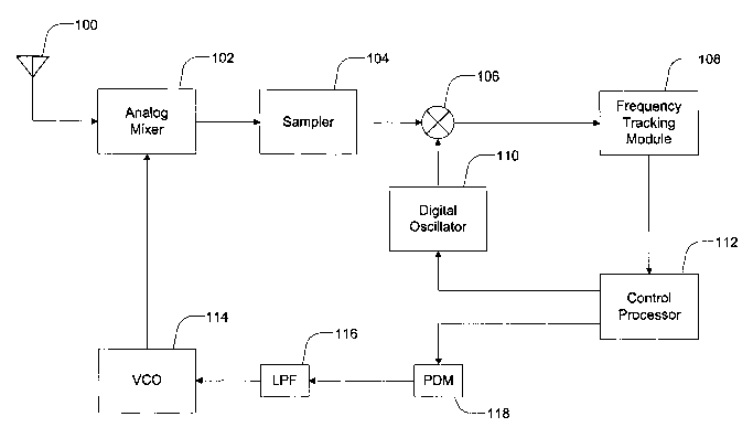
[1010] FIG. 1 shows a multiple-stage carrier frequency recovery apparatus;
[1011] FIG. 2 shows a frequency tracking module apparatus; and
[1012] FIG. 3 is a flowchart showing a method for adjusting downconverter
frequencies in a multiple-stage carrier frequency recovery system.
DETAILED DESCRIPTION
' [1013] A user terminal referred to herein may be mobile or stationary, and
may communicate with one or more base stations. A user terminal transmits
and receives data packets through one or more base stations. The base
stations are called modem pool transceivers. Each modem pool transceiver
may be connected to an HDR base station controller called a modem pool
controller (MPC). Modem pool transceivers and modem poor controllers are
parts of a network called an access network. The interconnected nodes of the
access network typically communicate with each other using fixed, land-based
connections such as T1 connections. An access network transports data
packets between multiple user terminals. The access network may be further
connected to additional networks outside the access network, such as a
corporate intranet or the Internet, and may transport data packets between
each
user terminal and such outside networks. A user terminal that has established
an active traffic channel connection with one or more modem pool transceivers
is called an active user terminal, and is said to be in a traffic state. A
user
terminal that is in the process of establishing an active traffic channel
connection with one or more modem pool transceivers is said to be in a
connection setup state. A user terminal may be any data device that
communicates through a wireless channel or through a wired channel, for
example using fiber optic or coaxial cables. A user terminal may further be
any
of a number of types of devices including but not limited to PC card, compact
flash, external or internal modem, or wireless or wireline phone. The
communication link through which the user terminal sends signals to the modem
pool transceiver is called a reverse link. The communication link through
which
CA 02466351 2004-05-06
WO 03/043180 PCT/US02/35877
a modem pool transceiver sends signals to a user terminal is called a forward
link.
[1014] FIG. 1 is a block diagram of an embodiment of an exemplary multiple-
stage carrier frequency recovery apparatus. In the embodiment shown, carrier
frequency recovery is divided into two stages, one using an analog carrier
signal
source 114 and another using a digital carrier signal source 110. An
embodiment may have more than two stages, or use different combinations of
analog and digital stages.
[1015] A signal is received through an antenna 100 and mixed with an
analog carrier signal in an analog mixer 102. The analog carrier signal is
generated by a variable-frequency signal source such as a voltage-controlled
oscillator (VCO) 114. The frequency of the carrier signal generated by the VCO
114 varies based on an input voltage. The input voltage is based on a digital
control signal provided by a control processor 112. In the exemplary
embodiment shown, the digital control signal is converted into an input
voltage
to the VCO 114 using a pulse density modulator (PDM) 118 and a low-pass
filter (LPF) 116. The PDM 118 receives a digital value from the control
processor 112 and outputs a train of pulses having a duty-cycle that is based
on
the digital value. The LPF 116 may be a simple RC circuit or an integrator or
any equivalent circuit. The LPF 116 converts the pulse train output by the PDM
118 into a DC voltage that determines the frequency,of the carrier signal
output
from the VCO 114. In an alternate embodiment, the PDM 118 and LPF 116 are
replaced with a simple digital-to-analog converter (DAC).
[1016] The resolution of the voltage adjustments that can be made at the
input to the VCO 114 is relatively coarse. In other words, a change of the
least-
significant bit in the digital value provided from the control processor 112
to the
PDM 118 may result in a relatively large change in the frequency of the
carrier
signal output by the VCO 114. Thus, the control processor 112 cannot
generally cause the frequency of the caPrier signal output by the VCO 114 to
match the carrier frequency of signal received through the antenna 100. Even
if
a high-resolution DAC is substituted for the LPF 116 and PDM 118, analog
noise at the input to the VCO 114 makes fine-tuning of the VCO output
frequency very inexact.
CA 02466351 2004-05-06
WO 03/043180 PCT/US02/35877
6
[1017] Because of the expected mismatch in frequency between the output
of the VCO 114 and the carrier frequency of the signal received through the
antenna 100, the output of the analog mixer 102 is generally not a pure
baseband signal. In other words, the signal output by the analog mixer 102
will
generally retain a low-frequency carrier component.
[1018] In the exemplary embodiment shown, the remaining low-frequency
carrier is separated from the desired baseband signal in the digital domain.
The
output of the analog mixer 102 is therefore digitally sampled in a sampler 104
and mixed with a low-frequency digital carrier in a digital mixer 106. The
output
of the digital mixer 106 is the downconverted baseband signal that is provided
to decoding circuitry known in the art such as filters, PN and/or Walsh
despreaders, deinterleavers, and decoders. The low-frequency digital carrier
is
generated by a digital oscillator 110. The frequency of the carrier generated
by
the digital .oscillator 110 can be adjusted with greater resolution than the
carrier
generated by VCO 114, although the VCO 114 can be adjusted over a wider
range of frequencies. For example, VCO 114 may be capable of producing
signals within a frequency range of +/- 45 megahertz in steps of 30 hertz,
where
digital oscillator 110 can produce signals with an arbitrarily fine resolution
and a
frequency range only limited by the analog to digital converter sampling
frequency. One skilled in the art will recognize that obvious variations using
different combinations of digital and analog frequency generators and mixers
are alternate embodiments of the embodiment described above.
[1019] In an exemplary embodiment, digital oscillator 110 is a digital rotator
capable of generating fine-resolution frequency and phase correction signals.
By increasing the number of bits used to represent the frequency and phase
inputs, a digital rotator can be readily designed to have greater frequency
and
phase resolution. In an alternative embodiment, digital oscillator 110 is a
direct
digital synthesizer (DDS). Digital oscillator 110 may also be any of a variety
of
other types of digital frequency reference generator. VCO 114 could be any of
a variety of voltage-controlled oscillators, including a temperature-
controlled
crystal oscillator (TCXO) or oven-controlled crystal oscillator (OCXO).
[1020] A frequency tracking module 108 measures the residual frequency
error in the signal output by digital mixer 106 and generates at least one
error
CA 02466351 2004-05-06
WO 03/043180 PCT/US02/35877
7
signal that is provided to a control processor 112. The control processor 112
uses the at least one error signal from the frequency tracking module 108 to
adjust control signals to the digital oscillator 110 and the PDM 118. By
changing the control signal provided to the PDM 118, the control processor 112
effects a change in the frequency of the signal output by the VCO 114.
[1021] In an exemplary embodiment, the control processor 112 controls the
output frequency of the VCO 114 such that the remaining frequency correction
needed is within a predetermined optimal or operational range of the digital
oscillator 110. For example, even where the digital oscillator 110 is capable
of
generating frequencies within a frequency band having a width of several
megahertz; the VCO 114 is adjusted such that the frequency of the digital
oscillator 110 may be maintained within a range having a width of 128 hertz.
Additionally; it may be desirable to keep the VCO frequency reference
relatively
close to the carrier frequency of the received signal. Adjusting the frequency
of
the VCO 114 to be as close as possible to the received carrier frequency will
tend to minimize the frequency of the signal output by the digital oscillator
110.
[1022] Also, in order to keep the digital oscillator 110 operating within its
optimal or operational frequency range, the control processor 112 increases
the
VCO 114 frequency and decreases the digital oscillator 110 frequency.
Conversely, where appropriate, the control processor 112 decreases the VCO
114 frequency and increases the digital oscillator 110 frequency.
[1023] In an exemplary embodiment, the control processor 112 adjusts the
coarse frequency in fixed frequency steps by changing a digital control signal
provided to the PDM 118. For example, if the PDM has a resolution of 30 Hz
per bit, the control processor 112 may increase the PDM control signal by 30,
60, or 90 Hz by changing the digital input value of the PDM by 1, 2, or 3. At
the
same time, the control processor 112 adjusts the control signal to the digital
oscillator 110 such that the output frequency of the digital oscillator 110 is
decreased by 30, 60, or 90 Hz. Due to the coarse resolution of the output of
the
VCO 114, the size of the frequency step for the VCO 114 can only be
estimated. In contrast, the size of the frequency step of the digital
oscillator 110
is very precise. Consequently, even after the digital oscillator 110 frequency
is
adjusted to compensate for a step change in VCO 114 frequency, the digital
CA 02466351 2004-05-06
WO 03/043180 PCT/US02/35877
8
oscillator 110 must generally be further adjusted before the output of the
digital
mixer 106 will have a frequency and phase that best matches that of the
received carrier signal.
[1024] FIG. 2 is a more detailed diagram of an embodiment of a frequency
tracking module 108 that is suitable for use in an HDR system. In an exemplary
embodiment, the receiver uses exclusively signals received within two pilot
bursts received within every slot. In HDR, for example, each slot is 1.667
milliseconds long, with one pilot burst centered within each half of the slot.
In
other words, each slot has a first pilot burst centered 417 microseconds from
the start of the slot and a second pilot burst centered 1.25 milliseconds from
the
start of the frame. In HDR, each pilot burst has a duration of 96 chips at a
chip
rate of 1.2288 megahertz. Before transmission, the pilot burst signals are
multiplied by a pseudonoise (PN) sequence. The frequency tracking module
108 shown in FIG. 2 serves to remove the PN component of the downconverted
baseband signal received from the digital mixer 106 and accumulates the
portion of the signal received within the pilot bursts.
[1025] A pilot burst chip clock 210 generates clock signals during the pilot
bursts of each received slot. The clock signals are provided to a PN generator
208 that then generates a PN signal having the same clock rate as the pilot
burst chip clock 210. That PN signal is then mixed with the downconverted
baseband signal in a digital mixer 202, to produce a PN despread pilot signal.
The PN despread pilot signal is then accumulated over the pilot burst period
in
an accumulator 204. The output of the accumulator 204 will be a phase error
signal corresponding to the phase error of the now fully demodulated pilot
signal. This phase error signal is then provided to a frequency tracking loop
(FTL) 108, which converts the phase error signal into a digital signal that
can be
used by the control processor 112. One of skill in the art would recognize
that
FTL 108 could be a first-order loop, a second-order loop, or other
configuration
of FTL.
[1026] In an exemplary embodiment, the frequency tracking module 108
generates one phase error estimate per slot using the two pilot burst periods
within the slot. In an alternate embodiment, the frequency tracking module 10S
generates more than one phase error estimate per slot. For example, the
CA 02466351 2004-05-06
WO 03/043180 PCT/US02/35877
9
frequency tracking module 108 may generate one phase error estimate for each
half-pilot-burst period, resulting in four phase error estimates. These phase
error estimates can then be used to estimate a rate of phase change, and thus
the remaining frequency error remaining in the baseband signal. Because of
the smaller sampling period used to generate each phase error estimate, phase
error measurements based on half of a pilot burst are more noisy than a single
estimate generated over two pilot burst periods. In another alternate
embodiment, one phase error estimate is generated for each pilot burst period
in a slot, resulting in two phase error estimates. In another alternate
embodiment, a single phase error estimate is generated using the pilot burst
periods over more than one slot. Because of aliasing concerns, the selection
of
number of phase error estimates over a number of slots represents a tradeoff
of
signal noise to the size of frequency error that can be detected. In an
alternate
embodiment, the frequency tracking module 108 can be configured by the
control processor 112 in real time to operate in any of several modes, wherein
each mode uses a different ratio of phase error estimates to slots.
[1027] In HDR, the pilot is spread using the all-one's code, so there is no
need for an explicit Walsh despreader between the digital mixer 202 and the
integrator 204. In an exemplary embodiment, the PN generator 208 generates
a complex PN code, and the digital mixer 202 is a complex multiplier. The
complex output of the digital mixer 202 is accumulated in the accumulator 204
in such a way that phase information is preserved in real and imaginary
portions
of the accumulated value.
[1028] FIG. 3 is a flowchart of an exemplary method for adjusting
downconverter frequencies in a multiple-stage carrier frequency recovery
system, such as shown in FIG. 1. During the operation of the carrier frequency
recovery system, the fine frequency value Ff is monitored at step 302 to
determine when it is operating within the optimal or operational frequency
range
of a fine frequency generation source, such as the digital oscillator 110
shown in
FIG. 1. At step 304, the fine frequency value Ff is tested to determine
whether
an adjustment should be made in the coarse frequency output of a coarse
frequency generation source, such as the VCO 114 shown in FIG. 2. If an
adjustment is necessary, then both Ff and Fc are adjusted at step 306. If no
CA 02466351 2004-05-06
WO 03/043180 PCT/US02/35877
adjustment is necessary, then the adjustment step of 306 is skipped. Within
step 306, if Ff is increased, then Fc is decreased by approximately the same
amount. If Ff is decreased, then Fc is increased by approximately the same
amount.
[1029] Those of skill in the art would understand that information and signals
may be represented using any of a variety of different technologies and
techniques. For example, data, instructions, commands, information, signals,
bits, symbols, and chips that may be referenced throughout the above
description may be represented by voltages, currents, electromagnetic waves,
magnetic fields or particles, optical fields or particles, or any combination
thereof.
[1030] Those of skill would further appreciate that the various illustrative
logical blocks, modules, circuits, and algorithm steps described in connection
with the embodiments disclosed herein may be implemented as electronic
hardware, computer software, or combinations of both. To clearly illustrate
this
interchangeability of hardware and software, various illustrative components,
blocks, modules, circuits, and steps have been described above generally in
terms of their functionality. Whether such functionality is implemented as
hardware or software depends upon the particular application and design
constraints imposed on the overall system. Skilled artisans may implement the
described functionality in varying ways for each particular application, but
such
implementation decisions should not be interpreted as causing a departure from
the scope of the present invention.
[1031] The various illustrative logical blocks, modules, and circuits
described
in connection with the embodiments disclosed herein may be implemented or
performed with a general purpose processor, a digital signal processor (DSP),
an application specific integrated circuit (ASIC), a field programmable gate
array
(FPGA) or other programmable logic device, discrete gate or transistor logic,
discrete hardware components, or any combination thereof designed to perform
the functions described herein. A general purpose processor may be a
microprocessor, but in the alternative, the processor may be any conventional
processor, controller, microcontroller, or state machine. A processor, such as
the control processor 112 described above, may also be implemented as a
CA 02466351 2004-05-06
WO 03/043180 PCT/US02/35877
11
combination of computing devices, e.g., a combination of a DSP and a
microprocessor, a plurality of microprocessors, one or more microprocessors in
conjunction with a DSP core, or any other such configuration.
[1032] The steps of a method or algorithm described in connection with the
embodiments disclosed herein may be embodied directly in hardware, in a
software module executed by a processor, or in a combination of the two. A
software module may reside in RAM memory, flash memory, ROM memory,
EPROM memory, EEPROM memory, registers, hard disk, a removable disk, a
CD-ROM, or any other form of storage medium known in the art. An exemplary
storage medium is coupled to the processor such the processor can read
information from, and write information to, the storage medium. In the
alternative, the storage medium may be integral to the processor. The
processor and the storage medium may reside in an ASIC. The ASIC may
reside in a user terminal. In the alternative, the processor and the storage
medium may reside as discrete components in a user terminal.
[1033] The previous description of the disclosed embodiments is provided to
enable any person skilled in the art to make or use the present invention.
Various modifications to these embodiments will be readily apparent to those
skilled in the art, and the generic~principles defined herein may be applied
to
other embodiments
[1034] without departing from the spirit or scope of the invention. Thus, the
present invention is not intended to be limited to the embodiments shown
herein
but is to be accorded the widest scope consistent with the principles and
novel
features disclosed herein.