Note : Les descriptions sont présentées dans la langue officielle dans laquelle elles ont été soumises.
CA 02466682 2006-02-13
1
A matrix-addressable optoelectronic apparatus and electrode means in
the same
The present invention concerns a matrix-addressable optoelectronic apparatus
comprising a functional medium in the form of an optoelectronically active
material provided in a global layer in sandwich between first and second
electrode means, each with parallel strip-like electrodes wherein the
electrodes of the second electrode means are oriented at an angle to the
electrodes of the first electrode means, wherein functional elements are
formed in volumes of the active material defined at respective overlaps
between the electrodes of the first electrode means and the electrodes of the
second electrode means to provide a matrix-addressable array with the
electrodes in contact with the active material, wherein a functional element
in
the active material can be activated by applying a voltage to the crossing
electrodes defining the element to form a light-emitting, light-absorbing,
reflecting or polarizing pixel in a display device, or alternatively by
incident
light to form a pixel in an optical detector and outputting a voltage or
current
via the electrodes crossing at the pixel, said active material in either case
being selected as an inorganic or organic material and capable according to
the intended function either to emit, absorb, reflect or polarize light upon
being a activated by an applied voltage or to output a voltage or current when
stimulated by incident light, or both, whereby the addressing of a pixel in
any
case takes place in a matrix-addressing scheme, and wherein the electrodes of
at least one of the electrode means are made of a transparent or translucent
material.
The present invention also concerns an electrodes means for use in the
matrix-addressable optoelectronic apparatus, comprising a thin-film electrode
layer with electrodes in the form of parallel strip-like electrical
conductors,
wherein the electrode layer is provided on an insulating surface of a
backplane.
The present invention particularly concerns apparatuses and devices
comprising functional elements in a planar array, wherein the functional
elements are addressed via respectively a first electrode means with parallel
strip-like electrodes arranged in contact with the functional elements on one
side thereof and another electrode means with similar electrodes, but oriented
perpendicular to the electrodes of the first means and provided in contact
with the opposite side of the functional element. This constitutes what is
CA 02466682 2006-02-13
2
called a matrix-addressable device. Such matrix-addressable devices can
comprise e.g. functional elements in the form of logic cells, memory cells or
in case of the present invention, pixels in a display or photodetector. The
functional elements may include one or more active switching means, in
which case the matrix-addressable device is termed an active
matrix-addressable device, or the functional elements may consist of passive
means only, e.g. resistive or capacitive means, in which case the
matrix-addressable device is termed a passive matrix-addressable device.
The latter is regarded as providing a most efficient way of addressing, for
instance in case of memory devices, as no switching elements, viz. transistors
are required in memory cell. It is then desirable to achieve as high storage
density as possible, but present design rules which set a lower limit to the
cell area, also limit the fill factor thereof, i.e. the area of the active
material
of the matrix-addressable apparatus that actually can be used for the
functional elements thereof.
A prior art passive matrix-addressable optoelectronic apparatus is shown in
fig. la and comprises an essentially planar global layer of optoelectronically
active material 3 in sandwich between a first electrode means EM 1
comprising parallel strip-like electrodes 1 of width w and spaced apart by a
distance d and a similar second electrode means EM2 comprising parallel
strip-like electrodes 2 of the same width w, but with the electrodes 2
arranged perpendicular to the electrodes 1 of the first electrode means EMI.
In the global layer of active material 3 the overlap between the electrodes 1,
2 of the respective electrode means defines a pixel 5 in the active material
3.
By applying voltage to the electrodes 1,2 crossing at this location, the pixel
5
will for instance emit light when the apparatus is configured as a display and
by applying incident light to the pixel 5, a detectable current will be output
on the electrodes 1,2 when the apparatus is configured as a photodetector.
Fig. 1b shows the prior art device of fig. la in a section taken along the
line
X-X making the layout of the electrodes 1,2 and the global layer of the
sandwiched active material 3 as well as the location of the pixels 5 apparent.
The active material 3 of the global layer usually has properties such that an
application of the voltage to crossing electrodes 1,2 only will affect the
pixel
5 at the crossing thereof and not neighbouring pixels or cells at the
electrodes
crossings in the vicinity of the former. This can be achieved by providing the
CA 02466682 2006-02-13
3
active material with anisotropic conducting property, such that electrical
conduction only can take place in a perpendicular direction to the surface of
the active material and between the overlapping electrodes, with no current
flowing through the global layer to the other pixels. The size and density of
pixels 5 will depend on a process-constrained minimum feature that can be
obtained in the manufacturing process. Such features are, e.g. when
electrodes are laid down as metallization which afterwards is patterned in a
microphotolithographic process resorting to microphotolithographic masks
and e.g. etching, dependent on the process-constrained smallest feature f that
can be defined by the mask and its value will in its turn depend on the
wavelength of the light used. In other words, this feature f will usually
within
the scope of today's technology be limited to say 0,15 - 0,2 ~.m, and hence
the width w of the electrodes 1,2 and the spacings therebetween will be of
about this magnitude.
In that connection it should be noted that the value 2f usually is termed the
pitch and that the maximum number of lines per unit length as obtainable
with prior art fabrication technology is given by the factor '/2f and
correspondingly the maximum number of features per unit area by the factor
'/4f2. Hence if the area 4 shown in fig. 1 is considered, it will be evident
that
the size of a pixel 5 is given by f2 as apparent from fig. 1 c which shows the
area 4 in greater detail. Each pixel 5 requires a real estate corresponding to
the area 4, the size of which is 4f2, in other words, four times larger than
the
area fz of the pixel. This consideration shows that the matrix in fig. 1 a has
a
fill factor of 0,25, i.e. f2/4fz. The degree of exploitation of the area
offered by
the layer 3 is thus low. In order to arrive at a higher fill factor or a
higher
density of pixels 5 in the global layer it would be desirable to increase
either
the fill factor or to obtain a higher resolution in the process-constrained
features of the matrix, e.g. into the sub-0,1 ~m range. However, although this
may increase the total number of pixels in a similar area, still it would not
be
able to guarantee a higher fill factor.
In view of the above considerations it is a major object of the present
invention to enable an increase of the fill factor in a matrix-addressable
optoelectronic apparatus of the afore-mentioned kind to a value approaching
unity and to achieve a maximum exploitation of the real estate offered by the
global layer of the active material 3 in such apparatuses without actually
being constrained by the actual or practical size of the process-constrained
CA 02466682 2006-02-13
4
minimum feature f, as the fill factor will not be influenced by decrease in f,
although such a decrease of course, will serve to further increase the
maximum number of pixels obtainable in a global layer of the active material
3.
The above objects as well as further features and advantages are achieved
according to the present invention with a matrix-addressable optoelectronic
apparatus which is characterized in that the electrodes of each electrode
means are provided in a respective electrode layer, that the electrodes in the
electrode means all have about the same width w, that electrodes of each
electrode means are mutually insulated electrically by an insulating thin film
of thickness 8, the magnitude of b being a fraction of the width w, and that
minimum magnitude of w is comparable to a process-constrained minimum
feature size f, whereby the fill factor of the pixels in the
optoelectronically
active material relative thereto is close to 1 and the number of pixels
approaches a maximum defined by the total area A of the active material
sandwiched between the electrode means, and said feature size f, said
maximum thus being defined by A/f2.
In an advantageous embodiment of the apparatus according to the invention,
the optoelectronically active material is an anisotropic conducting organic
material with diode domains contacting the electrodes of the electrode
means, and then the organic conducting material can preferably be a
conjugated light-emitting and/or photoelectric polymer, whereby the
matrix-addressable apparatus can be operated as a display or as a
photodetector or both.
In this advantageous embodiment of the apparatus according to the invention,
the diode domains can be capable of emitting light when stimulated by an
applied voltage, whereby the matrix-addressable apparatus can be operated as
a display, or the diode domains can be capable of outputting a current or
voltage when stimulated by incident light, whereby the matrix-addressable
apparatus can be operated as s photodetector.
The above objects as well as further features and advantages are also
achieved according to the present invention with an electrode means which is
characterized in that the thin-film electrode layer comprises
a first set of said strip-like electrodes of width wa and thickness ha
provided
on the backplane, the electrodes of the first set being mutually spaced apart
CA 02466682 2006-02-13
by distance d equal to or greater than wa, a second set of said strip-like
electrodes with width wb and thickness h6 provided in the spacings between
the electrodes of the first set and electrically insulated therefrom by a thin
film of an electrically insulating material with thickness 8 and at least
5 extending along the side edges of the parallel electrodes and forming an
insulating wall of thickness 8 therebetween, the magnitude of 8 being small
compared to the magnitude of either wa or w6, with the spacing distance d
between the electrodes of the first set being wb+28, and that the electrode
layer with electrodes and the insulating thin film forms a global planar layer
in the electrode means on the backplane thereof.
In an advantageous embodiment of the electrode means according to the
present invention the insulating walls between the electrodes of the first set
and the electrodes of the second set form portions of the thin film of
insulating material provided in a layer covering the side edges of the
electrodes of the first set up to the top surface thereof as well as the
backplane in the spacings between the former, and that the electrodes of the
second set are provided in recesses between the wall portions of the
insulating thin film and above a portion thereof covering the backplane, the
electrodes of the second set being flush with the top edge of the insulating
walls as well as the top surface of the electrodes of the first set, whereby
the
electrodes of the second set have the height hb = ha - 8, and that the
electrode
layer with electrodes and insulating material form a global planar layer of
thickness ha in the electrode means on the backplane thereof.
In at least one of the electrode means according to the invention the
electrodes as well as the backplane must be made of a transparent or a
translucent material, when the electrode means are used in the inventive
apparatus. The invention shall now be explained in more detail with
reference to exemplary embodiments in conjunction with the appended
drawing figures, of which
figs. la-c show a prior art matrix-addressable optoelectronic apparatus
exemplifying a conventionally attainable fill factor in such
apparatuses, as mentioned above,
fig. 2a a plan view of a matrix-addressable optoelectronic apparatus
according to the invention,
fig. 2b a section taken along line X-X in fig. 2a,
CA 02466682 2006-02-13
6
fig. 2c a detail of fig. 2a and illustrating the fill factor attainable with
the present invention,
fig. 3 a section through a first embodiment of the electrode means
according to the present invention,
fig. 4 a section through a second embodiment of the electrode means
according to the present invention,
fig. 5 schematically a cross section through light-emitting pixel as
used in the apparatus according to the present invention,
fig. 6 schematically a cross section through a light-detecting pixel as
used in the apparatus according the present invention, and
fig. 7 schematically the structure of a preferred optoelectronically
active material as used in the pixel in either fig. 5 and fig. 6.
With reference to figs. 2a, 2b and 2c a discussion shall now be given of an
apparatus according to the invention and including the electrode means of the
invention. From this discussion it shall then also become apparent how the
electrode means according to the invention shall allow the fill factor to
approach unity in an apparatus of this kind. A structurally similar apparatus,
but configured as a matrix-addressable ferroelectric memory device, is the
subject of for instance International published patent application
W003/041084 belonging to the same applicant as the present application.
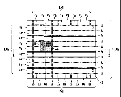
The apparatus according to the invention is shown in plan view in fig. 2a in
an embodiment which is restricted to a passive matrix-addressable
configuration wherein an optoelectronically active material 3 is deposited in
a global layer and sandwiched between two of the electrode means EM1,
EM2 according to the invention. The first electrode means EM 1 which could
be any of the embodiments shown in figs. 3 or 4, will be identical to the
second electrode means EM2 which, however, is provided with the parallel
strip-like electrodes 2 oriented at an angle and preferably perpendicular to
the corresponding electrodes 1 in the electrode means EM 1, as shown. Where
the electrodes 1,2 overlap, a pixel 5 is defined in the optoelectronically
active
material 3 therebetween. The pixel 5 can be a semiconducting inorganic or
organic material capable of emitting light or generating a photocurrent upon
an appropriate stimulation, e.g. by an applied voltage in the former case or
by
incident light in latter case. Most preferably the optoelectronically active
material shall be a conjugated polymer with an anisotropic electrical
conductivity, such that conduction only shall take place between overlapping
CA 02466682 2006-02-13
7
electrodes 1,2 and perpendicular to the plane of the layer of active material
3.
The driving, sensing and control circuitry are for clarity's sake not shown in
fig. 2a, but could in practical embodiments be implemented in CMOS
technology based on silicon and provided in the backplane 7 if this is made in
the same material. All electrodes 1,2 would then be suitably routed and
connected to said circuitry, in a manner well understood by persons skilled in
the art.
As mentioned, the active material 3 is sandwiched between the electrode
means EMI, EM2, as seen to advantage in fig. 2b which shows a section
through the apparatus in fig. 2a taken along the line X-X. At the overlap or
crossings of the electrodes 1,2 a pixel 5 is defined in the active material 3,
i.e. the light-emitting or photoconductive material. As the electrodes 1,2 in
the respective electrode means EMI, EM2 in any case are only separated by a
very thin wall 6a of insulating material, the thickness 8 of which being only
a
tiny fraction of that of the width w of the electrodes 1,2 and corresponding
most preferably to a process-constrained or process-definable minimum
feature f, it will be seen that the electrode means EM according to the
present
invention allows an increase in the fill factor towards unity. - It should be
noted that alternating electrodes in the electrode means EM, 1;2, the
electrodes ~a, ~b in any case may have different widths wa,wb, but as wa~wh,
their widths in practice can be considered having about the same value w.
This will be seen to advantage when one considers a planar section 4
comprising four pixels 51-54 as shown in fig. 2c. The area occupied by the
insulating walls 6a between the electrodes and the electrodes themselves are
defining the area of the pixels 51...54 in either electrode means EM 1, EM2 as
4f2 + 8f8 + 482. This implies that with 8 being only a tiny fraction of either
f
or the width w of the electrodes 1,2, the fill factor approaches unity in the
apparatus according to the invention, meaning that close to 100% of the area
of the active material 3 sandwiched between the electrode means EMl, EM2
is taken up by the pixels S, the average size of which will be f2. For
instance.
if f ~ w is set to unity and b = O,OIf, the area of the planar section will be
4 + 8 ~ 0.01 + 0,0004 ~ 4,08 and the fill factor becomes 4/4,08 = 0,98, i.e. a
fill factor of 98%. The maximum number of pixels 5 in the matrix, given that
the area of the accessible active material 3 is A, will then be close to AJf2
in
the apparatus according to the present invention. For instance, if the design
CA 02466682 2006-02-13
8
rule applied sets f = 0,2~,m, and an active material 3 area A is 106~.m,
0,98 ~ 106/0,22 = 24,5 ~ 106 addressable pixels 5 could be provided implying a
pixel density of about 25~ 106Jmm2. Wherein the electrodes as known in the
prior art are separated by a distance d defined by the minimum
process-constrained feature f, the planar section 4 shown in fig. 2c shall
only
contain one pixel 5 and the fill factor accordingly be 0,25 or 25%, while the
maximum number of pixels attainable then of course, will be '/4 of the
number that can be achieved with the apparatus according to the present
invention.
When the apparatus according to the invention as shown in figs. 2a-c is
configured as a as a display device, the active material 3 would then be
capable of light emission when stimulated by a voltage applied to the
respective crossing electrodes 1,2 of the electrode means EM1, EM2 and the
pixel 5 defined at the overlap between respective electrodes 1,2 would now
of course, be a pixel in the display. As the fill factor of course in any case
will approach unity, it will be possible to obtain a high resolution display
wherein the almost whole area A of the display is devoted to the pixels.
Moreover, an increase in the fill factor from say 0,25 towards I shall allow a
display with a correspondingly increased surface brightness. As the pixels at
least on one side of the display must be exposed to the exterior, this implies
that at least the electrodes I ;2 in one of the electrode means EM I ;EM2 must
be transparent or translucent and likewise the same shall apply to the
material
of one of the backplanes 7. In fig. 2b the backplane 7 could be realized with
circuitry for driving, sensing and control as mentioned, while an opposite
backplane 7' indicated by a stitched outline as well as the electrodes 2 must
be transparent or translucent to optical radiation. Also the insulating
material
used in the insulating thin film 6 could of course in such cases be
transparent
or translucent, and the electrodes 2 could e.g. as well-known by persons
skilled in the art be made of indium tin oxide (ITO) as commonly used in
light-emitting devices.
A first preferred embodiment of the electrode means EM is shown in fig. 3.
Herein the electrode means EM comprises the plurality of strip-like
electrodes Ea,~b provided on a backplane 7. The electrodes ~a can be
envisaged as belonging to a first set of electrode and formed from an applied
global layer of electrode material which subsequently are patterned in a
microphotolithographic step using a suitable mask, while the electrodes Eb
CA 02466682 2006-02-13
9
between the former can be regarded as belonging to a second set of
electrodes which are deposited after the application of the insulating wall
portion 6a and in the recesses between the electrodes ~a as generated in the
patterning steps thereof. The distance between two electrodes ~a is d, the
width of the electrodes ~a is wa, the width of the electrodes ~b is wb. Now
the
values wa,wb and the distance d have about a similar magnitude, the
minimum of which will be given by the process-constrained minimum feature
f obtainable in the patterning process for generating the electrodes Ea. At
the
same time the thickness 8 of the insulating wall portions 6a between the
electrodes ~a,Eb is not constrained by f and may have a thickness down to a
nanometre scale, with the only constraint to provide an insulating thin film
for preventing electrical faults and breakdown between the electrodes ~a,~b~
In other words, provided that the surface of the backplane 7 interfacing the
electrodes as required also is electrically insulating, all the parallel strip-
like
electrodes Ea,~b will be mutually electrically insulated. It should be noted
that a height of both ~a,~b as well as the insulating wall portion 6a is h and
one has the equation d = w6+2$. Provided that the distance d between the
electrodes is selected as wa+2d, the width wa;wb of the electrodes ~a;~b will
be the same and equal to the value w, all electrodes ~a,~b thus having the
same cross-section area and if made of the same conducting material ~, also
the same conducting properties.
In the embodiment of the electrode means EM according to the invention
shown in fig. 4 the electrodes ~a as are before formed in a patterning step
from a globally applied layer of electrode material and then the insulating
thin film 6 is deposited globally covering the substrate 7 and the electrodes
~a. A conducting material is now deposited filling the recesses and covering
the insulating layer 6b at bottom thereof between the electrodes ~a and then
in a subsequent planarization step the portion of the insulating thin film 6
covering the electrodes ~a as well as excess electrode material resulting from
the deposition of electrodes ~b are removed, leaving the electrodes ~a,~b
exposed in the surface of the electrode layer and flush with the top edge of
the wall portion 6a of the insulating thin film 6. All electrodes ~a,~b have
then exposed top surfaces and can form an ohmic contact with any applied
optoelectronically active material 3 thereabove, but as is the case a
capacitive
coupling may be had if the active material is dielectric, for instance a
liquid
CA 02466682 2006-02-13
crystal material, and in that particular circumstance, even the top surfaces
of
the electrodes 1,2 could be covered by the insulating thin film 6. This will
of
course apply to the above embodiment. The considerations regarding the
minimum width wa, wb of the electrodes ~a,~b are also valid here. Moreover
5 it will be seen that the height ha of an electrode sa differs from the
height hb
of an electrode sb by the amount b corresponding to the thickness 8 of the
portion 6b of the thin film 6 covering the substrate 7. This as before implies
that the distance d between the electrodes ~a must be increased in the
patterning process in order to obtain electrodes Ea,~b with equal cross
section
10 if that is desirable, e.g. for obtaining the same conducting capacity if
the
electrodes ~a,~b are made of conducting material with the same conductivity.
The planarization of the electrode layer of the electrode means EM according
to the invention can in both the embodiments as shown in figs. 3,4 can take
place by any suitable means, e.g. chemomechanical polishing, controlled
etching or a controlled micro-abrasive process. For detail concerning the
fabrication of the embodiments of the electrode means according to the
invention as depicted in figs. 3,4, and methods for their manufacture
reference may be made to the above-mentioned co-pending International
published patent application W003/041084.
Concerning the electrode materials for the electrode means EM as used in the
apparatus according to the invention, they could as mentioned be any suitable
conducting material, e.g. metals like titanium or aluminium, which commonly
are used in electronic devices. The electrode materials may also be organic
materials, for instance conducting polymers, but must then be compatible
with the process used for forming the insulating thin-film layer or any
process used for removing portions thereof. Further it is evident that the
electrodes of at least one of the electrode means EM must be transparent or
translucent to optical radiation, as mentioned, to enable the function of the
apparatus as a display or photodetector.
While it should be understood that the width w of the electrodes of the
electrode means EM according to the invention shall have a minimum value
defined by the process-constrained minimum feature f, it will of course in the
first instance only be the width of the electrodes ~a of the first set which
must
be formed by patterning, as well as the distance therebetween that is so
restricted. The electrodes ~b can be deposited by processes which are not
CA 02466682 2006-02-13
11
restricted by a design rule applying to the patterning process. The same of
course applies to the application of the insulating thin film which can take
place e.g. by oxidation, vapour deposition or spraying or sputtering down to
almost monoatomic dimensions. The only requirement is that it should
provide the necessary electrical insulation between the adjacent electrodes ~a
and ~b in the respective set s of electrodes in the electrode means EM. Also
while f in conventional photomicrolithographic processes usually would be in
the range of 0,2 ~m or somewhat less, other technologies presently
established or under development would allow features in the nanoscale
range, i.e. electrode widths down to a few tens of nanometres and for
instance the use of chemomechanical processing in the nanoscale range to
achieve the necessary planarization, which in any case would yield electrode
means EM with a top surface of high planarity and wherein all component
parts, i.e. electrodes ~a,~b as well as the insulating thin film 6 will be
flush in
the top surface.
Generally the use of the electrode means EM in the apparatus according to
the invention with the active medium sandwiched by two of the inventive
electrode means and the parallel strip-like electrodes oriented mutually at an
angle and preferably perpendicularly so as to form a matrix-addressable
display or a photodetector, shall allow a fill factor approaching unity and a
maximum number of definable pixels only constrained by the applicable
design rule for the patterning process of the .electrodes.
Fig. 5 shows schematically the structure of a single pixel in an embodiment
where the apparatus according to the invention is a display. Between an
electrode 1 of the first electrode means EM1 and an electrode 2 of the second
electrode means EM2 there is provided an optoelectronically active material
3 comprising light-emitting domains 10, preferably in the form of
light-emitting polymer diodes. The light-emitting polymer diodes 10 is
supplied with working voltage VE via the electrodes 1, 2 which are connected
to a power supply 8. It is to be understood that the electrodes 1, 2 of course
are part of the strip-like electrodes 1;2 of each of the electrode means
EM 1;EM2 such that electrode 2 in any case will be oriented preferably
perpendicular to electrode 1. The light-emitting diodes 10 could be
wavelength-tuneable and in that case the active material 3 would contain
light-emitting diodes wherein the wavelength is tuned by varying the voltage
CA 02466682 2006-02-13
12
VE as e.g. described in the International published patent application
W095/031515.
It should be noted that the apparatus according to the invention also could be
a non-emitting display, i.e. a display where the pixels in response to an
applied voltage may reflect, absorb or polarize light. This will be the case
when the optoelectronically active material is a liquid crystal material and
such displays are, of course, well-known in the art, but will by using the
electrode means according to the present invention gain the same advantages
as embodiments with light-emitting pixels. As the liquid crystal material is
dielectric, it should be noted that contacting top surfaces of the electrodes
of
the electrode means then actually could be covered by insulating thin film 6,
as already mentioned. In this regard reference may be made to the already
cited International published patent application, wherein relevant alternative
embodiments of the electrode means are disclosed.
Fig. 6 shows schematically a pixel 5 in an embodiment where the apparatus
according to the invention is an optical detector. The optoelectronically
active material 3 is similar to the light-emitting material in the embodiment
in fig. 5 and provided the sandwich between electrodes 1, 2 and oriented in
similar manner. The electrodes 1, 2 will when the active material 3 is
stimulated by incident light to generate a current or voltage, convey a signal
voltage VD to a sense amplifier 9.
It is of course, evident that at least one of the electrodes 1,2 in fig. 5 or
fig. 6
must be transparent and the same applies to the backplane (not shown) 7 on
which the electrode in case are provided. Concerning the optoelectronically
active material 3 this may as mentioned be either light-emitting diodes or
photoelectric diodes and particularly preferred are organic diodes of this
kind
based on conjugated polymers which as already mentioned have been
described in International published patent application W095/031515. It
should be noted that such light-emitting polymer diodes can be
wavelength-tuneable and emit light on several wavelengths by varying the
working voltage of the diode. In case such diodes also have photoelectric
properties and thus will be suited for application in a detector pixel as
shown
in fig. 6, it should be noted that their peak sensitivity wavelength will be
different from their peak emission wavelength and shifted towards shorter
wavelengths than those of the optical emission. This is the phenomenon
CA 02466682 2006-02-13
13
termed Stokes shift, as well-known to skilled persons The diodes of the
optoelectronically active material may be manufactured as a polymer thin
film with domains of conjugated polymers and with a thickness of a few tens
of nanometres and even less. The size of the individual diodes shall not be
much larger.
A pixel may contain a number of physically separated light-emitting or
light-absorbing domains 10, 10', as illustrated in fig. 7 which may be
regarded as a schematic cross section through a single pixel 5 in the
apparatus according to the invention. Of course the layer 3 of active material
forms part of a global layer therein with the domains 10, 10' each being only
one type of light-emitting polymer or light-absorbing polymer, with different
emitting or absorbing wavelength bands. Moreover, the conjugated polymer
thin film can be anisotropic electrical conducting and hence a current applied
to the layer of active material sandwiched between the electrodes 1,2 will
only flow between the electrodes defining each separate pixel S and not in
the transversal direction. To obtain the full effect of the light emission or
a
photovoltaic effect, all the domains 10,10', whether being light-emitting or
light-absorbing, should contact the electrodes 1,2, and it will be seen that
in
the inventive apparatus with electrode means EM according to the invention
and with the fill factor approaching unity this will actually be the case,
such
that in the apparatus according to the invention either can provide a display
with maximum surface brightness or a photodetector with maximum
sensitivity, as is the case. Moreover, it is also evident that the ensuing
high
fill factor due to the thickness 8 of the insulating material 6 being only a
tiny
fraction of the electrode width w will allow a very high pixel density and an
effective pixel area approaching the total area A of the global layer of
active
material 3. Also the resolution or the degree of pixellation, i.e. the number
of
pixels obtainable in the apparatus, will attain the maximum allowed by the
magnitude of the process-constrained minimum feature f. In sum any of the
considerations above serve to emphasize the radical increase in performance
that will be obtainable with the apparatus according to the present invention,
whether it is configured as a display or as an optical detector.
When configured as a display it can be both a monochrome or a colour
display. In the latter case, the active material could comprise diode domains
10, 10' emitting on different wavelengths, depending on the working voltage
VE applied. For instance an increase in VE would shift the dominant emission
CA 02466682 2006-02-13
14
toward shorter wavelengths, provided that diode domains 10,10' having their
peak emission in e.g. the red and blue range of the optical radiation
spectrum,
respectively. In other words, wavelength tuning of a single pixel is in this
case obtained by changing the voltage VE applied thereto via the electrodes
1,2 contacting the pixel.
Also as mentioned the active material could be a liquid crystal material, in
which case the pixels, of course, would upon stimulation either could be
reflecting, light-absorbing or polarizing, as well-known to persons skilled in
the art.
When configured as an optical detector, the apparatus could be used to
advantage as the detector of an optoelectronic camera, and mutatis mutandis
enable a colour camera, with diode domains 10,10' having different
wavelength sensitivity and generating a current response or voltage VD with
components dependent of the wavelength of the incident light. The high
resolution, i.e. the high degree of pixellation of the inventive apparatus,
would then be comparable to that of a conventional photographic film which
in a 24x36 mm format may have more than 3~ 10' pixels depending on the
properties of the emulsion, thus attaining a linear resolution in the order of
5 qm. Scaling an optical detector according to the invention with regard to
its
degree of pixellation a 1.2 x 1.2 mm detector chip designed with f = 0,20qm
would yield the same performance as the 24x36 mm film format. However,
when the apparatus according to the present invention is used as an optical
detector in an electronic camera, one should keep in mind that the effective
pixel size must be compatible with the wavelength ~, of the incident length,
i.e. at least '/2~,, in other words for the range from ultraviolet to near
infrared,
about 0,1 ~ to 1,0 ~.. This of course, implies that the effective area of the
active material and the size of the detector must be correspondingly adjusted
to obtain a resolution comparable with that of available photographic
emulsions.