Note : Les descriptions sont présentées dans la langue officielle dans laquelle elles ont été soumises.
CA 02467526 2004-03-O1
WO 03/021921 PCT/EP02/06072
TITLE: ELECTRONIC DEVICES AND CASING CONSTRUCTIONS FOR
SUCH DEVICES
S
Field of the Invention
This invention relates to electronic devices and
casing constructions for such devices.
Background of the Invention
In the electronics industry, especially in the
audio - video - computer - communications (AVCC) sector,
there is a constant drive to reduce the size and weight
of products and to make them more easily portable. One
of the ways in which this is achieved is to use suitably
lightweight and strong materials as constructional
materials.
Plastics materials with and without reinforcement
have for many years been widely used as constructional
materials for electronic devices. However, metallic
materials, especially magnesium based materials, have
started to find uses for this application. Magnesium has
a density which is roughly two thirds that of aluminium
and is only slightly higher than that of fibre
reinforced plastics yet has excellent mechanical and
physical properties as well as good processibility and
recyclability.~Magnesium based materials potentially
offer other benefits in the electronics industry, such
as good shielding from electromagnetic interference
(EMI) and good thermal conductivity which facilitates
heat dissipation from components, e.g. when contained in
a case made of the material. Thus, magnesium based
CA 02467526 2004-03-O1
WO 03/021921 PCT/EP02/06072
2
materials are seen as attractive alternatives to
plastics materials for use as constuctional materials in
the electronics industry, especially the AVCC sector.
However, magnesium is a very malleable material and
casing structures made from magnesium based materials
may be easily deformed especially when a device which is
encased by the material is dropped or otherwise
mishandled and therefore subjected to external
mechanical shock. This may easily lead to damage of
components of an electronic device encased within a
magnesium alloy casing.
The present invention seeks to provide a novel
improved casing structure for an electronic device.
Summary of the invention
According to the present invention in a first aspect
there is provided a casing structure for an electronic
device comprising a carrier against which one or more of
the device components may be fitted, the carrier having
a first carrier face and a second carrier face, a first
cover adapted to attach to the carrier to form a first
enclosure over at least part of the first carrier face
and a second cover adapted to attach to the carrier to
form a second enclosure over at least part of the second
carrier face, wherein the carrier has a receptacle for
receiving the first and second covers, the receptacle
having a first recess for receiving a rim of the first
cover and a second recess for receiving a rim of the
second cover, the receptacle having in at least one of
the first and second recesses a cushioning layer for
cushioning the cover received in the recess.
CA 02467526 2004-03-O1
WO 03/021921 PCT/EP02/06072
3
The first and second faces of the carrier may
conveniently be on opposite sides of the carrier and may
point in mutually opposite directions.
The said receptacle may be formed separately from the
carrier and attached thereto but preferably the
receptacle is formed integrally with the carrier. For
example, the carrier including the receptacle preferably
comprises a substantially rigid part made of moulded
plastics material.
The receptacle desirably extends around the carrier
at an edge or periphery thereof. The receptacle may form
a closed loop around the edge or edges of the carrier.
The first recess and the second recess are
conveniently on mutually opposite sides of the
receptacle. For example, the first recess may be
provided in the receptacle on the same side of the
carrier as a front face of the carrier and the second
recess may be provided in the receptacle on a rear face
of the carrier.
The receptacle may conveniently have, at least in the
parts thereof which are adjacent to the recesses, a
cross-sectional shape which approximates to a letter H.
In the casing according to the invention the
cushioning layer may comprise a strip of elastomeric
material. The kind of material used as the elastomeric
material is not critical, but the material selected
should give good cushioning and resilience. For example,
the material may be a silicone rubber.
Preferably, a cushioning layer is provided in both of
the first and second recesses. Such layers may comprise
CA 02467526 2004-03-O1
WO 03/021921 PCT/EP02/06072
4
two cushioning rings manufactured separately and fitted
into the recesses during assembly of the device.
In the casing construction according to the first
aspect of the invention the first and second covers may
usefully comprise metallic material. The metallic
material may be a magnesium based material, e.g. a
material such as an alloy containing at least 80%, in
many cases at least 95%, by weight magnesium.
In the casing according to the first aspect of the
invention, the first and and second recesses of the
receptacle may provide push fits for rims of the first
and second covers respectively. The first and second
covers may also have attachments to the carrier
additional to that provided by the receptacle. For
example, the first cover and the carrier on its first
face may have complementary formations which facilitate
attachment of the first cover to the carrier and the
second cover and the carrier on its second face may have
complemetary formations which facilitate attachment of
the second cover to the carrier. The respective
complementary formations may conveniently provide push
fits, especially tight fits, of the first and second
covers to the carrier, the first and second covers when
attached to the carrier thereby being clamped thereto.
The complementary formations may for example be
cylindrical holes and plugs which fit therein. For
example, such holes may be provided in the carrier in
corner regions thereof and complementary plugs may be
provided on the inner faces of the covers.
The casing construction according to the invention
may be such that at least one of the faces of the
CA 02467526 2004-03-O1
WO 03/021921 PCT/EP02/06072
carrier has a wall providing an internal protection zone
to one or more sensitive components of the electronic
device. The wall may form in shape a closed loop figure.
A layer of cushioning material may be provided on the
5 inside of the wall. The layer may comprise a rubber
ring.
According to the present invention in a second aspect
there is provided an electronic device having a casing
structure according to the first aspect. The device may
for example be a hand held portable device. The device
may for example comprise a radio communications unit,
such as a terminal for the transmission and receipt of
data and/or speech signals and/or video or other picture
signals.
The device may incorporate standard components to
provide these operations. For example, the device may
include as components fitted against the carrier one or
more printed circuit boards carrying keyboard, processor
and radio circuit components, an electro-optical display
such as a liquid crystal display and optionally an
electro-optical scanner, an antenna and optionally a
microphone and a speaker. One or more of these
components such as the electro-optical display which is
regarded as particularly sensitive to mechanical shock
may be enclosed within an internally cushioned region as
well as protected externally by the casing structure
according to the first aspect or the invention. The
carrier may have formations such as clips on its faces
which allow the device components to be fitted thereto
in a known manner. The antenna where included may
conveniently be housed in an antenna housing fitted to
CA 02467526 2004-03-O1
WO 03/021921 PCT/EP02/06072
6
the carrier at an edge region of the carrier. The
antenna may extend from the housing inside an enclosed
region between the carrier and one of the covers.
The present invention provides a more rugged
electronic device construction using suitable
lightweight materials than is available in the prior
art, especially for relatively complex hand held
portable devices such as radio communications terminals
which may optionally incorporate computing units. In
particular, the invention allows use of magnesium based
material to be used in the construction thereby taking
advantage of the benefits provided by magnesium, without
the problems caused by easy deformity. In particular,
the invention is effective in protecting a device having
outer covers made of magnesium based material from
external shock such as caused by dropping. In one
embodiment the invention can provide two levels of shock
resistance to the most sensitive components of the
device by providing both internal and external
cushioning layers.
We have found in practical tests using the invention
that devices made with magnesium based outer covers can
be dropped and can withstand shocks caused thereby
equivalent to 70008 and that such devices are highly
attractive to users.
Other advantages of the invention are that it allows
easy, rapid and inexpensive assembly of the device from
its components and easy access to the components during
use.
CA 02467526 2004-03-O1
WO 03/021921 PCT/EP02/06072
7
Embodiments of the present invention will now be
described by way of example with reference to the
accompanying drawings, in which:
Brief description of the accompanying drawings
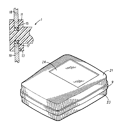
Fig 1 is a perspective front view of a carrier for
use in the construction of an electronic device.
Fig 2 is a cross sectional view (in the plane
indicated by the lines II - II viewed in the direction
X) of part of the rim structure of the carrier shown in
Fig 1.
Fig 3 shows the rim structure of Fig 2 with parts of
the rims of covers shown fitted thereon.
Fig 4 is a perspective view of a construction
comprising the carrier of Fig 1 with covers fitted
thereon.
Fig 5 is a partly cut away perspective view of the
construction of Fig 4 with some of the internal
components of the device when partly assembled shown
fitted against the front face of the carrier of the
construction.
Fig 6 shows the construction of Fig 5 with a
keybooard receptacle component also fitted.
Fig 7 is a partly cut away perspective view of the
construction of Fig 4 with components of the device
shown fitted against the rear face of the carrier of the
construction.
Description of illustrative embodiments of the invention
As shown in Fig 1, a carrier 1 moulded from rigid
and strong plastics material is provided. The carrier 1
CA 02467526 2004-03-O1
WO 03/021921 PCT/EP02/06072
8
forms the basic body structure of a portable hand held
electronic device, namely a radio communications
terminal for transmitting data to and from a remote
control centre (not shown) and for displaying data such
as that sent and received, all in a manner known in the
art. The carrier 1 is generally in the form of a flat
plate having front and rear faces pointing in opposite
directions with projections formed on the faces to
provide certain component retaining functions. A front
face only is shown in Fig 1. As seen in Fig 1, the shape
of the plate forming the carrier 1 is generally
rhomboidal with rounded edges and corners. The front
face of the carrier 1 has a rectangular wall 5
protruding therefrom and formed integrally therewith in
the moulding and a rectangular shaped cushioning strip 7
of soft rubber material is provided inside the wall 5
and lies along the inner edges of the wall 5. The wall 5
and strip 7 provide an internal shock protective barrier
for delicate components to be fitted in a region 8
inside the wall as described later. A further region 10
for reception of less delicate components of the device
is provided on the front face beneath the region 8. The
carrier 1 has an integrally moulded rim structure 9
which runs around the entire periphery of the carrier 1.
As shown in more detail in Fig 2, the rim structure 9
is formed at the periphery of the carrier 1. The rim
structure 9 has a shape which approximates to the shape
of a letter H in cross section. The rim structure 9
provides a portion of enlarged thickness on the carrier
1 in which is formed a first recess 11 in a front facing
part of the rim structure 9 and a second recess 13 in a
CA 02467526 2004-03-O1
WO 03/021921 PCT/EP02/06072
9
rear facing part of the rim structure 9. The recesses 11
and 13 run around the entire periphery of the carrier 1
in the rim portion 9. A silicone rubber cushioning ring
15 fits inside the recess 11 and a silicone rubber
cushioning ring 17 fits inside the recess 13.
In use, magnesium alloy outer covers are fitted on
the carrier 1 when all of the internal device components
have been fitted thereon as illustrated later. Rims of
the covers are engaged in the receptacle provided by the
rim structure 9 of the carrier 1 and the recesses 11 and
13 therein. Figure 3 shows the peripheral part of the
carrier 1 with a rim 18 of an upper magnesium alloy
cover fitted inside the recess 11 and cushioned by the
ring 15 and a rim 19 of a lower magnesium alloy cover
fitted inside the recess 13.
Fig 4 shows the completed outer structure of the
device with a front magnesium alloy cover 21 fitted over
the front face of the carrier 1 and a rear magnesium
alloy cover 23 fitted over the rear face of the carrier
1, the covers 21 and 23 having the rims 18 and 19
(Figure 3) which respectively fit into the recesses 11
and 13 of the rim portion 9 of the carrier 1. The cover
21 has a window portion 24 through which a display can
be viewed. The display is one of the components fitted
inside the device against the carrier 1 as described
later.
The rim portion 9 of the carrier 1 and the magnesium
alloy covers 21 and 23 fitted thereon provide an
excellent protective shield for internal components of
the electronic device if the device is accidently
dropped or otherwise subjected to a mechanical shock
CA 02467526 2004-03-O1
WO 03/021921 PCT/EP02/06072
during use. Deformation of the magnesium alloy covers 21
and 23 is prevented or resisted by the cushioning effect
of the rings 15 and 17 in the recesses 11 and 13 on the
rims 17 and 19 respectively.
S Figs 5,6 and 7 illustrate components which may be
present in the device when the covers 21 and 23 are
fitted on the carrier 1. Fig 5 shows a partially
completed assembly of components on the the carrier 1
on the front face thereof. A window 25 is fitted in the
10 region 8 provided by the wall 5 and strip 7 shown in
Figure 1. Circuit components 27 are fitted in the
region 10 of the front face beneath the window 25. An
antenna housing 29 is fitted on the carrier 1 in a
peripheral region above the window 25. An antenna is
1$ fitted inside the antenna housing 29 and has pins 31
extending from the antenna housing 29 generally in a
plane parallel to the front face of the carrier 1. The
pins 31 are attached to an antenna portion (not shown)
inside the antenna housing 29 which comprises a
conducting plate perpendicular to the plane of the pins
31.
As seen in Fig 6, a circuit board 33 comprising a
keyboard receptacle is fitted over the circuit
components 27. For simplicity, the antenna housing 29
but not the antenna is shown in Figure 6.
As shown in Fig 7, the rear face of the carrier 1 has
fitted thereon a printed circuit board 35 on which
various electronic processors and circuit components are
carried. These components provide the electronic memory,
computing and control functions and radio transmitter
and receiver parts of the electronic device. A liquid
CA 02467526 2004-03-O1
WO 03/021921 PCT/EP02/06072
11
cystal display 37 is fitted against the rear face of the
carrier 1. The rear face only of the display 37 is seen
in Fig 7. The front of the liquid crystal display 37 is
covered by the window 25 shown in Figs 5 and 6.
Figs 5, 6 and 7 also show cylindrical recesses 39
formed in the carrier 1 in corner regions thereof on the
upper and lower faces of the carrier 1. These recesses
39 engage complementary studs (not shown) on the inner
faces of the covers thereby providing attachment of the
covers to the carrier 1 in addition to the attachment
provided by the recesses 11 and 13.