Sélection de la langue

Search

Sommaire du brevet 2467632 

Énoncé de désistement de responsabilité concernant l'information provenant de tiers

Une partie des informations de ce site Web a été fournie par des sources externes. Le gouvernement du Canada n'assume aucune responsabilité concernant la précision, l'actualité ou la fiabilité des informations fournies par les sources externes. Les utilisateurs qui désirent employer cette information devraient consulter directement la source des informations. Le contenu fourni par les sources externes n'est pas assujetti aux exigences sur les langues officielles, la protection des renseignements personnels et l'accessibilité.

Disponibilité de l'Abrégé et des Revendications

L'apparition de différences dans le texte et l'image des Revendications et de l'Abrégé dépend du moment auquel le document est publié. Les textes des Revendications et de l'Abrégé sont affichés :

  • lorsque la demande peut être examinée par le public;
  • lorsque le brevet est émis (délivrance).
(12) Demande de brevet: (11) CA 2467632
(54) Titre français: STATION DE BASE DOTEE D'UNE INTERFACE DE BUS EN SERIE/EN PARALLELE HYBRIDE
(54) Titre anglais: BASE STATION HAVING A HYBRID PARALLEL/SERIAL BUS INTERFACE
Statut: Réputée abandonnée et au-delà du délai pour le rétablissement - en attente de la réponse à l’avis de communication rejetée
Données bibliographiques
(51) Classification internationale des brevets (CIB):
  • G06F 13/14 (2006.01)
  • G06F 13/00 (2006.01)
  • G06F 13/38 (2006.01)
  • G06F 13/40 (2006.01)
  • H03M 9/00 (2006.01)
(72) Inventeurs :
  • GREDONE, JOSEPH (Etats-Unis d'Amérique)
  • STUFFLET, ALFRED (Etats-Unis d'Amérique)
  • AXNESS, TIMOTHY A. (Etats-Unis d'Amérique)
(73) Titulaires :
  • INTERDIGITAL TECHNOLOGY CORPORATION
(71) Demandeurs :
  • INTERDIGITAL TECHNOLOGY CORPORATION (Etats-Unis d'Amérique)
(74) Agent: SMART & BIGGAR LP
(74) Co-agent:
(45) Délivré:
(86) Date de dépôt PCT: 2002-11-19
(87) Mise à la disponibilité du public: 2003-06-05
Requête d'examen: 2004-05-19
Licence disponible: S.O.
Cédé au domaine public: S.O.
(25) Langue des documents déposés: Anglais

Traité de coopération en matière de brevets (PCT): Oui
(86) Numéro de la demande PCT: PCT/US2002/037150
(87) Numéro de publication internationale PCT: WO 2003046391
(85) Entrée nationale: 2004-05-19

(30) Données de priorité de la demande:
Numéro de la demande Pays / territoire Date
09/990,060 (Etats-Unis d'Amérique) 2001-11-21
10/081,466 (Etats-Unis d'Amérique) 2002-02-22

Abrégés

Abrégé français

L'invention concerne une interface de bus en parallèle/en série hybride destinée à une station de base et possédant un dispositif de démultiplexage de bloc de données. Ce dispositif présente une entrée configurée pour recevoir un bloc de données et permet de démultiplexer le bloc de données en une pluralité de quartets. Pour chaque quartet, un convertisseur parallèle-série permet de convertir le quartet en données sérielles. Une ligne permet de transférer les données sérielles de chaque quartet. Un convertisseur parallèle-série sert à convertir les données sérielles de chaque quartet, afin de récupérer ce quartet. Un dispositif de reconstruction de bloc de données sert à combiner les quartets récupérés dans le bloc de données.


Abrégé anglais


A hybrid serial/parallel bus interface for a base station has a data block
demultiplexing device (40). The data block demultiplexing device has an input
configured to receive a data block and demultiplexes the data block into a
plurality of nibbles. For each nibble, a parallel to serial converter (42)
converts the nibble into serial data. A line (44) transfers each nibble's
serial data. A serial to parallel converter (46) converts each nibble's serial
data to recover that nibble. A data block reconstruction device (48) combines
the recovered nibbles into the data block.

Revendications

Note : Les revendications sont présentées dans la langue officielle dans laquelle elles ont été soumises.


CLAIMS
What is claimed is:
1. A hybrid serial/parallel bus interface for a base station comprising:
a data block demultiplexing device having an input configured to receive a
data
block and demultiplexing the data block into a plurality of nibbles, each
nibble having
a plurality of bits;
for each nibble:
a parallel to serial converter for converting that nibble into serial data;
a line for transferring that nibble serial data; and
a serial to parallel converter for converting that nibble serial data to
recover that nibble; and
a data block reconstruction device for combining the recovered nibbles
into the data block.
2. The base station interface of claim 1 wherein a number of bits in a data
block is N and a number of the lines is i and 1 < i < N.
3. The base station interface of claim 1 wherein a number of bits in a nibble
is four and a number of lines is two.
4. A hybrid serial/parallel bus interface for a base station comprising:
means having an input configured to receive a data block for
demultiplexing the data block into a plurality of nibbles, each nibble having
a plurality
of bits;
for each nibble:
means for converting that nibble into serial data;
a line for transferring that nibble serial data; and

means for converting that nibble serial data to recover that nibble;
and
means for combining the recovered nibbles into the data block.
5. The base station interface of claim 4 wherein a number of bits in a data
block is N and a number of the lines is i and 1 < i < N.
6. The base station interface of claim 4 wherein a number of bits in a nibble
is four and a number of lines is two.
7. A base station having hybrid serial/parallel bus interface for transferring
data from a first node to a second node, the interface comprising:
a data block demultiplexing device for demultiplexing a data block from the
first node into m sets of n bits and for adding a start bit to each of the m
sets, the m
start bits collectively representing one of a particular function to be
performed or a
destination;
for each of the m sets, a separate line for transferring that set of the m
sets from
the first node to the second node;
a data block reconstruction device for receiving the m sets, for combining the
m
sets into the data block and for utilizing the m sets in accordance with the m
start bits.
8. The base station interface of claim 7 wherein the demultiplexing device
sets at least one of the m start bits in a one state when transmitting data
and when the
interface is not transmitting data, maintains all the separate lines in a zero
state.
9. The base station interface of claim 7 wherein the m start bits represent a
start of data transfer.
11

10. The base station interface of claim 7 wherein the m start bits
collectively
represent a particular function to be performed and not a destination.
11. The base station interface of claim 7 wherein functions that the m start
bits collectively represent include a relative increase, a relative decrease
and an
absolute value function.
12. The base station interface of claim 7 wherein the m start bits
collectively
represent a particular destination and not a function to be performed.
13. The base station interface of claim 12 wherein destinations that the m
start bits collectively represent include an RX and TX gain controller.
14. The base station interface of claim 7 wherein the m start bits
collectively
represent both a particular function to be performed and a particular
destination.
15. A base station having a hybrid serial/parallel bus interface for
transferring data from a first node to a second node, the interface
comprising:
means for demultiplexing a data block into m sets of n bits;
means for adding a start bit to each of the m sets, the m start bits
collectively
representing one of a particular function to be performed or destination;
means for transferring from the first node each of the m sets over a separate
line;
means for receiving at the second node each of the transferred m sets; and
means for utilizing the received m sets in accordance with the m start bits.
12

16. The base station interface of claim 15 wherein the adding means sets at
least one of the m start bits to a one state and when the interface is not
transmitting
data, all the separate lines to a zero state.
17. The base station interface of claim 15 wherein at least one of the m start
bits represents a start of data transfer.
18. The base station interface of claim 15 wherein the m start bits
collectively represent a particular function to be performed and not a
destination.
19. The base station interface of claim 15 wherein functions that the m start
bits collectively represent include a relative increase, a relative decrease
and an
absolute value function.
20. The base station interface of claim 15 wherein the m start bits
collectively represent a particular destination and not a function to be
performed.
21. The base station interface of claim 20 wherein destinations that the m
start bits collectively represent include an RX and TX gain controller.
22. The base station interface of claim 15 wherein the m start bits
collectively represent both a particular function to be performed and a
particular
destination.
23. A base station hybrid serial/parallel bus interface for use in a
synchronous system, the synchronous system having an associated clock, the bus
interface, comprising:
13

a data block demultiplexing device having an input for receiving a data block
and demultiplexing the data block into a plurality of nibbles, each nibble
having a
plurality of bits;
an even and an odd set of parallel to serial (P/S) converters, each set of P/S
converters receiving the nibbles synchronous with a clock rate of the clock,
and for
converting the nibbles into a serial data;
a first set of i multiplexers for serially transferring data from the set of
even P/S
converters on a positive edge of the clock over i lines and serially
transferring data
from the set of the odd P/S converters on a negative edge of the clock over i
lines;
a second set of i demultiplexers for receiving the even and odd serial data
and
sending the even received serial data to an even buffer and the odd serial
data to an odd
buffer;
an even and an odd set of serial to parallel (S/P) converters, the even set of
S/P
converters converting the received even serial data to even parallel data and
outputting
the even parallel data synchronous with the clock;
the odd set of S/P converters for converting the odd received serial data to
odd
parallel data and outputting the odd parallel data synchronous with the clock;
and
a data block reconstruction device for combining the even and odd parallel
data
as the data block.
24. The base station interface of claim 23 wherein each data block has N bits
and <IMG>
25. The base station interface of claim 23 wherein the even and the odd
buffers respectively buffer the outputs of the even and odd set of P/S
converters so that
the even and odd set of S/P converters receive the even and odd received
serial data
synchronous with the clock.
14

26. A bi-directional serial/parallel bus interface employed by a base station
comprising:
a plurality of lines for transferring data blocks, the plurality of lines
being less
than a number of bits in each data block;
a first node sending first data blocks to a second node over the plurality of
lines,
the first node demultiplexing the data block into a plurality of first
nibbles, the plurality
of first nibbles being equal in number to the plurality of lines, each first
nibble having a
plurality of bits; and
the second node sending second data blocks to the first node over the
plurality
of lines, the second node demultiplexing the data block into a plurality of
second
nibbles, the plurality of second nibbles being equal in number to the
plurality of lines,
each second nibble having a plurality of bits.
27. The base station interface of claim 26 wherein the first node demultiplex
the data block into a plurality of third nibbles, a number j of the third
nibbles is less
than the number N of lines and transferring the third nibbles over j lines.
28. The base station interface of claim 27 wherein the second node
demultiplexes fourth data blocks into K bits, where K is less than or equal to
N-j lines,
and transferring the fourth data block over K lines.
29. The base station interface of claim 26 wherein the first node data blocks
include gain control information.
30. The base station of claim 29 wherein the second node data blocks include
an acknowledgment of receipt of the gain control information.

31. The base station interface of claim 29 wherein the second node data
blocks include information of a status associated with the second node.
32. A gain control (GC) employed by a base station, comprising:
a GC controller for producing a data block having n bits representing a gain
value;
i lines for transferring the data block from the GC controller to a GC, where
1 <i<n; and
the GC for receiving the data block and adjusting a gain of the GC using the
gain value of the data block.
33. The base station GC of claim 32 further comprising:
a data block demultiplexing device for demultiplexing the data block into a
plurality of nibbles, each nibble being transferred over a different line of
the i lines;
and
a data block reconstruction device for combining the nibbles into the data
block.
34. The base station GC of claim 33 wherein appended to each nibble is a
start bit.
35. The base station GC of claim 34 wherein the start bits indicate a function
to be performed.
36. The base station GC of claim 35 wherein mathematical functions
indicated by the start bits include a relative increase, a relative decrease
and an
absolute value function.
16

37. The base station GC of claim 34 wherein the GC includes a RX GC and a
TX GC and the start bits indicate whether the data block is sent to the RX GC
or TX
GC.
17

Description

Note : Les descriptions sont présentées dans la langue officielle dans laquelle elles ont été soumises.


CA 02467632 2004-05-19
WO 03/046391 PCT/US02/37150
[0001] BASE STATION HAVING A HYBRID
PARALLELISERIAL BUS INTERFACE
[0002] BACKGROUND
[0003] The invention relates to bus data transfers. In particular, the
invention
relates to reducing the number of lines used to transfer bus data.
[0004] One example of a bus used to transfer data is shown in Figure 1. Figure
1 is an illustration of a receive and transmit gain controllers (GCs) 30, 32
and a GC
controller 38 for use in a wireless communication system. A communication
station,
such as a base station or user equipment, transmits (TX) and receives (RX)
signals. To
control the gain of these signals, to be within the operating ranges of other
reception/transmission components, the GCs 30, 32 adjust the gain on the RX
and TX
signals.
[0005] To control the gain parameters for the GCs 30, 32, a GC controller 38
is
used. As shown in Figure l, the GC controller 38 uses a power control bus,
such as a
sixteen line bus 34, 36, to send a gain value for the TX 36 and RX 34 signals,
such as
eight lines for each. Although the power control bus lines 34, 36 allow for a
fast data
transfer, it requires either many pins on the GCs 30, 32 and the GC controller
38 or
many connections between the GCs 30, 32 and GC controller 38 on an integrated
circuit (IC), such as an application specific IC (ASIC). Increasing the number
ofpins
requires additional circuit board space and connections. Increasing IC
connections
uses valuable IC space. The large number of pins or connections may increase
the cost
of a bus depending on the implementation.
[0006] Accordingly, it is desirable to have other data transfer approaches.
[0007] ~ SUMMARY
[0008] A hybrid serial/parallel bus interface has a data block demultiplexing
device.
The data bloclc demultiplexing device has an input configured to receive a
data block and
demultiplexes the data bloclc into a plurality of nibbles. For each nibble, a
parallel to serial
converter converts the nibble into serial data. A line transfers each nibble's
serial data. A

CA 02467632 2004-05-19
WO 03/046391 PCT/US02/37150
serial to parallel converter converts each nibble's serial data to recover
that nibble. A data
block reconstruction device combines the recovered nibbles into the data
block.
[0009] BRIEF DESCRIPTION OF THE DRAWINGS)
[0010] Figure 1 is an illustration of a RX and TX GC and a GC controller.
[0011] Figure 2 is a bloclc diagram of a hybrid parallel/serial bus interface.
[0012] Figure 3 is a flow chart for transferring data blocks using a hybrid
parallel/serial bus interface.
[0013] Figure 4 illustrates demultiplexing a blocl~ into a most significant
and
least significant nibble.
[0014] Figure 5 illustrates demultiplexing a block using data interleaving.
[0015] Figure 6 is a block diagram of a bi-directional hybrid parallel/serial
bus
interface.
[0016] Figure 7 is a diagram of an implementation of one bi-directional line.
[0017] Figure 8 is a timing diagram illustrating start bits.
[0018] Figure 9 is a bloclc diagram of a function controllable hybrid
parallel/serial bus interface.
[0019] Figure 10 is a timing diagram of start bits for a function controllable
hybrid parallel/serial bus interface.
[0020] Figure 11 is a table of an implementation of start bits indicating
functions.
[0021] Figure 12 is a block diagram of a destination controlling hybrid
parallel/serial bus interface.
[0022] Figure 13 is a table of an implementation of start bits indicating
destinations.
[0023] Figure 14 is a table of an implementation of start bits indicating
destinations/functions.
2

CA 02467632 2004-05-19
WO 03/046391 PCT/US02/37150
[0024] Figure 15 is a block diagram of a destinations/functions controlling
hybrid parallel/serial bus interface.
[0025] Figure 16 is a flow chart for start bits indicating
destinations/functions.
[0026] Figure 17 is a bloclc diagram for a positive and negative clock edge
hybrid parallel/serial bus interface.
[0027] Figure 18 is a timing diagram for a positive and negative clock edge
hybrid parallel/serial bus interface.
[0028] Figure 19 is a block diagram of a 2-line GC/GC controller bus.
[0029] Figure 20 is a block diagram of a 3-line GC/GC controller bus.
[0030] DETAILED DESCRIPTION OF THE PREFERRED EMBODIMENTS)
[0031 ] Figure 2 is a bloclc diagram of a hybrid parallel/serial bus interface
and
Figure 3 is a flow chart of hybrid parallel/serial bus interface data
transfer. A data
block is to be transferred across the interface i 44 from node 1 50 to node 2
52. A data
block demultiplexing device 40 receives the block and demultiplexes it into i
nibbles
for transfer over i data transfer lines 44, (56). The value for i is based on
a tradeoff
between number of connections and transfer speed. One approach to determine i
is to
first determine a maximum latency permitted to transfer the data bloclc. Based
on the
allowed maximum latency, a minimum number of lines required to transfer the
block is
determined. Using the minimum number of lines, the lines used to transfer the
data is
selected to be at least the minimum. The lines 44 may be the pins and their
associated
connections on a circuit board or connections on an IC. One approach to
demultiplex
into nibbles divides the bloclc into a most significant to a least significant
nibble. To
illustrate for an eight bit block transfer over two lines as shown in Figure
4, the block
is demultiplexed into a four bit most significant nibble and a four bit least
significant
nibble.
[0032] Another approach interleaves the block across the i nibbles. The first
i
bits of the block become the first bit in each nibble. The second i bits
become the
3

CA 02467632 2004-05-19
WO 03/046391 PCT/US02/37150
second bit in each nibble and so on until the last i bits. To illustrate for
an eight bit
block over two connections as shown in Figure 5, the first bit is mapped to
the first bit
of nibble one. The second bit is mapped to the first bit of nibble two. The
third bit is
mapped to the second bit of nibble one and so on until the last bit is mapped
to the last
bit of nibble two.
[0033] Each nibble is sent to a corresponding one of i parallel to serial
(P/S)
converters 42, (58), convened from parallel bits to serial bits, and
transferred serially
across its line, (60). On the opposing end of each line is a serial to
parallel (S/P)
converter 46. Each S/P converter 46 converts the transmitted serial data into
its
original nibble, (62). The i recovered nibbles are processed by a data block
reconstruction device 48 to reconstruct the original data block, (64).
[0034] In another, bidirectional, approach, the i connections are used to
transfer
data in both directions as shown in Figure 6. Information data may be
transferred in
both directions or information may be sent in one direction and an
acknowledgment
sent baclc in the other direction. A data block for transfer from node 1 50 to
node 2 52
is received by the data block demultiplexing and reconstruction device 66. The
demultiplexing and reconstruction device 66 demultiplexes the block into i
nibbles. i
P/S converters 68 convert each nibble into serial data. A set of multiplexers
(MUXs)/DEMUXs 71 couples each P/S converter 68 to a corresponding one of the i
lines 44. At node 2 52, another set of MUXs/DEMUXs 75 connects the lines 44 to
a
set of S/P converters 72. The S/P converters 72 convert the received serial
data of each
nibble into the originally transmitted nibbles. The received nibbles are
reconstructed
by a data block demultiplexing and reconstruction device 76 into the original
data
bloclc and output as the received data block.
[0035] For bloclcs transferred from Node 2 52 to Node 1 50, a data block is
received by the data block demultiplexing and reconstruction device 76. That
block is
demultiplexed into nibbles and the nibbles are sent to a set of P/S converters
74. The
P/S converters 74 convert each nibble into serial format for transfer across
the i lines
4

CA 02467632 2004-05-19
WO 03/046391 PCT/US02/37150
44. A Node 2 set of MUXs/DEMUXs 75 couples the P/S converters 74 to the i
lines
44 and a Node 1 set of MUXs/DEMUXs 71 couples the lines 44 to i S/P converters
70.
The S/P converters 70 convert the transmitted data into its original nibbles.
The data
block demultiplexing and reconstruction device 66 reconstructs the data block
from the
received nibbles to output the received data block. Since data is only sent in
one
direction at a time, this implementation operates in a half duplex mode.
[0036] Figure 7 is a simplified diagram of one implementation ofbidirectional
switching circuits. The serial output from the node 1 P/S converter 68 is
input into a
tri-statable buffer 78. The buffer 78 has another input coupled to a voltage
representing a high state. The output of the buffer 78 is the serial data
which is sent via
the line 85 to a Node 2 tri-statable buffer 84. A resistor 86 is coupled
between the line
85 and ground. The Node 2 buffer 84 passes the serial data to a Node 2 S/P
converter
72. Similarly, the serial output from the Node 2 P/S converter 74 is input
into a tri-
statable buffer 72. That buffer 72 also having another input coupled to a high
voltage.
The serial output of that buffer 82 is sent via the line 85 to a Node 1 tri-
statable buffer
80. The Node 1 buffer 80 passes the serial data to a Node 1 S/P converter 70.
[0037] In another implementation, some of the i lines 44 may transfer data in
one direction and the other i lines 44 transfer data in another direction. At
Node 1 50,
a data bloclc is received for transmission to Node 2 52. Based on the data
throughput
rate required for the block and the traffic demand in the opposite direction,
j, being a
value from 1 to i, of the connections are used to transfer the block. The
block is
broken into j nibbles and converted to j sets of serial data using j of the i
P/S converters
68. A corresponding number of j Node 2 S/P converters 72 and the Node 2 data
block
separation and reconstruction device 76 recovers the data block. In the
opposite
direction, up to i j or k lines are used to transfer block data.
[0038] In a preferred implementation of the bidirectional bus for use in a
gain
control bus, a gain control value is sent in one direction and an
acknowledgment signal

CA 02467632 2004-05-19
WO 03/046391 PCT/US02/37150
is sent back. Alternately, a gain control value is sent in one direction and a
status of
the gain control device in the other direction.
[0039] One implementation of the hybrid parallel/serial interface is in a
synchronous system and is described in conjunction with Figure 8. A
synchronous
clock is used to synchronize the timing of the various components. To indicate
the
start of the data bloclc transfer, a start bit is sent. As shown in Figure 8,
each line is at
its normal zero level. A start bit is sent indicating the beginning of the
block transfer.
In this example, all the lines send a start bit, although it is only necessary
to send a start
bit over one line. If a start bit, such as a one value, is sent over any line,
the receiving
node realizes that the block data transfer has begun. Each serial nibble is
sent through
its corresponding line. After transfer of the nibbles, the lines return to
their normal
state, such as all low.
[0040] In another implementation, the start bits are also used as an indicator
of
functions to be performed. An illustration of such an implementation is shown
in
Figure 9. As shown in Figure 10, if any of the connections's first bits are a
one, the
receiving node realizes block data is to be transferred. As shown in the table
of Figure
11 for a GC controller implementation, three combinations of start bits are
used, "O1,"
"10" and "11." "00" indicates a start bit was not sent. Each combination
represents a
function. In this illustration, "01" indicates that a relative decrease
function should be
performed, such as decreasing the data block value by 1. A "10" indicates that
a
relative increase function should be performed, such as increasing the data
block value
by 1. A "11" indicates an absolute value function, where the block maintains
the same
value. To increase the number of available functions, additional bits are
used. For
example, 2 starting bits per line are mapped to up to seven (7) functions or n
starting
bits for i lines are mapped up to i"+ 1 _ 1 functions. The processing device
86 performs
the function on the received data block as indicated by the starting bits.
[0041 ] In another implementation as shown in Figure 12, the start bits
indicate a
destination device. As illustrated in Figure 13 for a two destination
device/two line
6

CA 02467632 2004-05-19
WO 03/046391 PCT/US02/37150
implementation, the combination of start bits relates to a destination device
88-92 for
the transferred data block. A "O1" represents device 1; a "10" represents
device 2; and
a "11" represents device 3. After receipt of the start bits of the data block
reconstruction device 48, the reconstructed block is sent to the corresponding
device
88-92. To increase the number of potential destination devices, additional
start bits
may be used. For n starting bits over each of i lines, up to i"+ 1 _ 1 devices
are selected.
[0042] As illustrated in the table of Figure 14, the start bits may be used to
represent both function and destination device. Figure 14 shows a three
connection
system having two devices, such as a RX and TX GC. Using the start bit for
each line,
three functions for two devices is shown. In this example, the start bit for
line 3
represents the target device, a "0" for device 1 and a "1" for device 2. The
bits for
connections 2 and 3 represent the performed function. A "11" represents an
absolute
value function; a "10" represents a relative increase function; and a "O1"
represents a
relative decrease. All three start bits as a zero, "000," is the normal non-
data transfer
state and "001" is not used. Additional bits may be used to add more functions
or
devices. For n starting bits over each of i lines, up to i"+i _ 1
functiol~/device
combinations are possible.
[0043] Figure 15 is a block diagram for a system implementing the start bits
indicating both function and destination device. The recovered nibbles are
received by
the data bloclc reconstruction device 48. Based on the received start bits,
the
processing device 86 performs the indicated function and the processed block
is sent to
the indicated destination device 88-92.
[0044] As shown in the flow chart of Figure 16, the start bits indicating the
function/destination are added to each nibble, (94). The nibbles are sent via
the i lines,
(96). Using the start bits, the proper function is performed on the data
block, the data
bloclc is sent to the appropriate destination or both, (98).
[0045] To increase the throughput in a synchronous system, both the positive
(even) and negative (odd) edge of the clock are used to transfer block data.
One
7

CA 02467632 2004-05-19
WO 03/046391 PCT/US02/37150
implementation is shown in Figure 17. The data block is received by a data
block
demultiplexing device 100 and demultiplexed into two (even and odd) sets of i
nibbles.
Each set of the i nibbles is sent to a respective set of i P/S devices 102,
104. As shown
in Figure 17, an odd P/S device set 102, having i P/S devices, has its clock
signal
inverted by an invertor 118. As a result, the inverted clock signal is half a
clock cycle
delayed with respect to the system clock. A set of i MUXs 106 select at twice
the
clock rate between the even P/S device set 104 and the odd P/S device set 102.
The
resulting data transferred over each connection is at twice the clock rate. At
the other
end of each connection is a corresponding DEMUR 108. The DEMUXs 108
sequentially couple each line 44 to an even 112 and odd 110 buffer, at twice
the clock
rate. Each buffer 112, 110 receives a corresponding even and odd bit and holds
that
value for a full clock cycle. An even 116 and odd 114 set of S/P devices
recover the
even and odd nibbles. A data block reconstruction device 122 reconstructs the
data
bloclc from the transferred nibbles.
[0046] Figure 18 illustrates the data transfer over a line of a system using
the
positive and negative clock edge. Even data and odd data to be transferred
over line 1
is shown. The hatching indicates the negative clock edge data in the combined
signal
and no hatching the even. As shown, the data transfer rate is increased by
two.
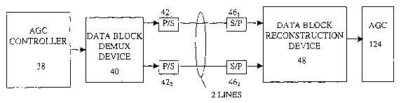
[0047] Figure 19 is a preferred implementation of the hybrid parallel/serial
interface used between a GC controller 3 8 and a GC 124. A data bloclc, such
as having
16 bits of GC control data (8 bits RX and 8 bits TX), is sent from the GC
contTOller 38
to a data block demultiplexing device 40. The data block is demultiplexed into
two
nibbles, such as two eight bit nibbles. A start bit is added to each nibble,
such as
malting 9 bits per nibble. The two nibbles are transferred over two lines
using two P/S
converters 42. The S/P converters 46z upon detecting the start bitsZ convert
the
received nibbles to parallel format. The data block reconstruction device
reconstructs
the original 16 bits to control the gain of the GC 124. If a function is
indicated by the
8

CA 02467632 2004-05-19
WO 03/046391 PCT/US02/37150
start bits, such as in Figure 11, the AGC 124 performs that function on the
received
block prior to adjusting the gain.
[0048] Figure 20 is another preferred implementation for a hybrid
parallel/serial
converter, using three (3) lines, between a GC controller 38 and a RX GC 30
and TX
GC 32. The GC controller 38 sends a data block to the GC 30, 32 with proper RX
and
TX gain values and start bits, such as per Figure 14. If the start bits per
Figure 14 are
used, Device 1 is the RX GC 30 and Device 2 is the TX GC 32. The data block
demultiplexing device 40 demultiplexes the data block into three nibbles for
transfer
over the three lines. Using the three P/S converters 42 and three S/P
converters 46, the
nibbles are transferred serially over the lines and converted into the
original nibbles.
The data block reconstruction device 48 reconstructs the original data block
and
performs the function as indicated by the start bits, such as relative
increase, relative
decrease and absolute value. The resulting data is sent to either the RX or TX
GC 30,
32 as indicated by the start bits.
* *
9

Dessin représentatif
Une figure unique qui représente un dessin illustrant l'invention.
États administratifs

2024-08-01 : Dans le cadre de la transition vers les Brevets de nouvelle génération (BNG), la base de données sur les brevets canadiens (BDBC) contient désormais un Historique d'événement plus détaillé, qui reproduit le Journal des événements de notre nouvelle solution interne.

Veuillez noter que les événements débutant par « Inactive : » se réfèrent à des événements qui ne sont plus utilisés dans notre nouvelle solution interne.

Pour une meilleure compréhension de l'état de la demande ou brevet qui figure sur cette page, la rubrique Mise en garde , et les descriptions de Brevet , Historique d'événement , Taxes périodiques et Historique des paiements devraient être consultées.

Historique d'événement

Description Date
Inactive : CIB du SCB 2022-09-10
Inactive : CIB expirée 2022-01-01
Demande non rétablie avant l'échéance 2009-11-19
Le délai pour l'annulation est expiré 2009-11-19
Inactive : CIB expirée 2009-01-01
Réputée abandonnée - omission de répondre à un avis sur les taxes pour le maintien en état 2008-11-19
Inactive : CIB de MCD 2006-03-12
Modification reçue - modification volontaire 2006-02-20
Modification reçue - modification volontaire 2005-03-07
Modification reçue - modification volontaire 2004-09-28
Inactive : IPRP reçu 2004-09-14
Inactive : Page couverture publiée 2004-07-23
Lettre envoyée 2004-07-21
Inactive : Acc. récept. de l'entrée phase nat. - RE 2004-07-21
Lettre envoyée 2004-07-21
Demande reçue - PCT 2004-06-21
Exigences pour l'entrée dans la phase nationale - jugée conforme 2004-05-19
Exigences pour une requête d'examen - jugée conforme 2004-05-19
Toutes les exigences pour l'examen - jugée conforme 2004-05-19
Exigences pour l'entrée dans la phase nationale - jugée conforme 2004-05-19
Demande publiée (accessible au public) 2003-06-05

Historique d'abandonnement

Date d'abandonnement Raison Date de rétablissement
2008-11-19

Taxes périodiques

Le dernier paiement a été reçu le 2007-10-12

Avis : Si le paiement en totalité n'a pas été reçu au plus tard à la date indiquée, une taxe supplémentaire peut être imposée, soit une des taxes suivantes :

  • taxe de rétablissement ;
  • taxe pour paiement en souffrance ; ou
  • taxe additionnelle pour le renversement d'une péremption réputée.

Veuillez vous référer à la page web des taxes sur les brevets de l'OPIC pour voir tous les montants actuels des taxes.

Historique des taxes

Type de taxes Anniversaire Échéance Date payée
Enregistrement d'un document 2004-05-19
Requête d'examen - générale 2004-05-19
Taxe nationale de base - générale 2004-05-19
TM (demande, 2e anniv.) - générale 02 2004-11-19 2004-10-15
TM (demande, 3e anniv.) - générale 03 2005-11-21 2005-10-18
TM (demande, 4e anniv.) - générale 04 2006-11-20 2006-10-18
TM (demande, 5e anniv.) - générale 05 2007-11-19 2007-10-12
Titulaires au dossier

Les titulaires actuels et antérieures au dossier sont affichés en ordre alphabétique.

Titulaires actuels au dossier
INTERDIGITAL TECHNOLOGY CORPORATION
Titulaires antérieures au dossier
ALFRED STUFFLET
JOSEPH GREDONE
TIMOTHY A. AXNESS
Les propriétaires antérieurs qui ne figurent pas dans la liste des « Propriétaires au dossier » apparaîtront dans d'autres documents au dossier.
Documents

Pour visionner les fichiers sélectionnés, entrer le code reCAPTCHA :


Pour visualiser une image, cliquer sur un lien dans la colonne description du document. Pour télécharger l'image (les images), cliquer l'une ou plusieurs cases à cocher dans la première colonne et ensuite cliquer sur le bouton "Télécharger sélection en format PDF (archive Zip)" ou le bouton "Télécharger sélection (en un fichier PDF fusionné)".

Liste des documents de brevet publiés et non publiés sur la BDBC .

Si vous avez des difficultés à accéder au contenu, veuillez communiquer avec le Centre de services à la clientèle au 1-866-997-1936, ou envoyer un courriel au Centre de service à la clientèle de l'OPIC.


Description du
Document 
Date
(aaaa-mm-jj) 
Nombre de pages   Taille de l'image (Ko) 
Description 2004-05-19 9 469
Dessins 2004-05-19 8 203
Dessin représentatif 2004-05-19 1 7
Revendications 2004-05-19 8 265
Abrégé 2004-05-19 1 59
Page couverture 2004-07-23 1 37
Accusé de réception de la requête d'examen 2004-07-21 1 177
Rappel de taxe de maintien due 2004-07-21 1 111
Avis d'entree dans la phase nationale 2004-07-21 1 202
Courtoisie - Certificat d'enregistrement (document(s) connexe(s)) 2004-07-21 1 105
Courtoisie - Lettre d'abandon (taxe de maintien en état) 2009-01-14 1 173
PCT 2004-05-19 2 80
PCT 2004-05-20 3 139
Taxes 2004-10-15 1 28
Taxes 2005-10-18 1 28
Taxes 2006-10-18 1 29
Taxes 2007-10-12 1 29