Note : Les descriptions sont présentées dans la langue officielle dans laquelle elles ont été soumises.
CA 02467668 2004-05-18
WO 03/047304 PCT/EPO1/13996
OPTICAL SPACE-SWITCHING MATRIX
The present invention relates to an acousto-optical space-switching matrix. In
particular
the present invention relates to an optical spatial switching matrix
comprising N input
ports and M output ports, in which it is possible to switch an optical beam
from any of the
input ports to any of the output ports.
Acousto-optical based switches have been proposed in the past.
US patent 6,016,216 describes a polarization independent acousto-optic tunable
filter
(PIAOTF) used for multi-wavelength switching and routing in wavelength
division
multiplexing (WDM) networks. In the PIAOTF an incident unpolarized light beam
is
divided to propagate and to be diffracted along two polarization division
branches. By
using polarization converters and equal optical paths for the two polarization
division
channels, a PIAOTF is created which minimizes polarization dependent loss and
polarization mode dispersion. Furthermore, a preferred embodiment of the AOTF
using an
elongated acousto-optic interaction medium is described that provides the
additional
advantages of narrow bandwidth, lower drive power and easier alignment.
US patent N° 5,909,304 proposes an acousto-optic tunable filter based
on an isotropic
acousto-optic diffraction medium excited with an acoustic wave generated from
a phased
array transducer. Said acoustic-wave causes a diffraction of an incident light
into said
acousto-optic diffraction medium in a way to obtain a frequency of the
diffracted light,
which is narrower than the optical frequencies of said incident light.
US patent N° 5.852,688 describes a method for optical energy transfer
and energy
guidance using an electric field to control energy propagation using a class
of poled
structures in solid material. The poled structures, which may form gratings in
thin film or
bulk configurations, may be combined with waveguide structures. Electric
fields are
applied to the poled structures to control routing of optical energy.
Techniques include
frequency-selective switchable and adjustable-tunable reflection, splitting,
directional
1
CONFIRMATION COPY
CA 02467668 2004-05-18
WO 03/047304 PCT/EPO1/13996
coupling, frequency-tunable switching and efficient beam combining, as well as
polarized
beam combining. Adjustable tunability is obtained by a poled structure, which
produces a
spatial gradient in a variable index of refraction along an axis in the
presence of a variable
electric field. In one embodiment, the patent describes a method of switching
a grating
which consists of a poled material with an alternating domain structure of
specific period.
When an electric field is applied across the periodic structure, a Bragg
grating is formed
by the electro-optic effect, reflecting optical radiation with a certain
bandwidth around a
center wavelength. The grating may be used by itself, or in combination with
other
gratings to form integrated structures in a ferroelectric crystal.
Specifically of interest is a
method of using an integrated structure in which one or more optical
waveguides interact
with one or more periodic structures to form a wavelength selective integrated
optical
switch.
US 5457556 describes an optical cross-comlect system in which incoming and
outgoing
fiber optic trunks carrying WTDM signals are terminated to first inlet ports
and first outlet
ports of an optical space switch. A wavelength division demultiplexer is
connected to a
second outlet port of the optical space switch and a wavelength division
multiplexes is
connected to a second inlet port of the optical space switch. A wavelength-
divided space
switch has first inlet ports connected to the outputs of the wavelength
division
demultiplexer and first outlet ports comlected to the inputs of the wavelength
division
multiplexes. A time division demultiplexer is connected to a second outlet
port of the
wavelength-divided space switch and.a time division multiplexes is connected
to a second
inlet port of the wavelength-divided space switch. The outputs of the time
division
demultiplexer are connected to first inlet ports of a time switch and the
inputs of the time
division multiplexes are connected to first outlet ports of the time switch.
The time switch
has second inlet ports and second outlet ports connected to a switched network
US patent N° 4,995,693 proposes an array of acousto-optic Bragg cells
to couple one of a
plurality of input light sources, or channels, to one out of a plurality of
output terminals, or
channels. By choice of the radio frequency tunable control, any of the inputs
can be
coupled to any of the outputs, by means of scan lenses.
2
CA 02467668 2004-05-18
WO 03/047304 PCT/EPO1/13996
Applicant has observed that the major disadvantage using acousto-optic Bragg
cells is the
dependence on the SOP of the efficiency of the switching process, since, the
input
geometry being kept fixed as radio frequency is tuned, in order to widen the
diffraction
angle on which the phase-matching condition can be reached up to a first order
approximation, anisotropic diffraction must be employed. Moreover, a, since
radio-
frequency at about 100MHz is used to allow acceptable diffraction efficiency,
diffraction
angles in the range of degree are obtained. In this manner for minimizing the
losses, for
example the crosstalk between a channel and an adjacent channel, several
centimeters of
free-space propagation must be provided between the switching element and the
output
ports, resulting in the structure to be sensitive to thermo-mechanical
perturbations.
Applicant has noted that said medium may change the state of polarization of
the optical
beam in relationship with said change of the frequency of the acoustic wave.
Applicant has tackled the problem of realizing a switching matrix architecture
in which
any commutation operation realized by means of acoustic waves is not dependent
on the
state of polarization of the optical beams and is not achieved by a change of
frequency of
said acoustic waves.
Applicant has found that if each switching element of a switching matrix
performs the
connection between one predetermined input port and one predetermined output
port, each
commutation can be activated if and only if a connection between said input
and said
output ports is required. This in principle minimizes energy consumption. In
general, a
MxN matrix can be considered, connecting M input ports to N output ports.
Applicant proposes a design for acousto-optic switching elements. Switching
elements are
designed so that when a switching element is active, a portion of the incident
light beam is
deflected preferably at 90 degrees with respect to the input beam. This 90-
degree
deflection if reached with a fixed frequency. Working at 90 degrees enable to
keep a
closely-packed architecture and to minimize the beam propagation necessary to
obtain
good channel rejection.
In dependence on the overall functional destination of the matrix, the
percentage in power
of the input beam to be switched can be adjusted by proper design of the
switching
3
CA 02467668 2004-05-18
WO 03/047304 PCT/EPO1/13996
component.
A first aspect of the present invention regards an optical switch matrix
comprising:
at least an input matrix port defining at least a row of said matrix,
a plurality of output matrix ports defining columns of said matrix,
a plurality of switching element each one being disposed at the intersection
of said at least
one row and one of said columns,
characterized in which
each of said plurality of switch elements in a predetermined position of the
matrix, in an
activated condition, connects an input matrix port to an output matrix port,
said ports
being correspondents respectively to said predetermined position of the
matrix, and
each of said plurality of switch elements comprises an acousto-optic deflector
to select one
of said plurality output matrix port.
Preferably, for each switching element in said activated condition the matrix
includes at
least one further switching element inactive in the same matrix row and in a
successive
column.
Preferably, said matrix further comprising a substrate on which said switching
element are
provided and a plurality of waveguides in which the optical signals from input
ports to
switching elements and from switching elements to output ports are guided.
A further aspect of the present invention regards optical switch comprising:
at least one input port,
a plurality of output ports,
an acousto optic medium,
a switching mechanism which activates said switch by generating acoustic waves
in said
acousto optic medium,
characterized in that it comprises
a semi-transparent interface which partially reflects and partially transmits
an optical
beam, said transmitted beam being sent from said at least one input port to
one of said
plurality of output ports ,
said reflected beam being diffracted from said acousto-optic medium when
activated by
4
CA 02467668 2004-05-18
WO 03/047304 PCT/EPO1/13996
said switching mechanism, from at least one input port to another one port of
said plurality
of output ports.
Said switch further comprising a first prism and a second prism, realized in
an acousto-
optic medium, bonded each other in a way to form said semi-transparent
interface.
Preferably, said semi-transparent interface comprises at least an optical
conductive
medium.
Preferably, said acousto-optic diffraction medium is an isotropic acousto
optic diffraction
medium.
Preferably, said switching mechanism comprises a piezo electric transducer.
Preferably, said piezo electric transducer comprises a piezo-electric
transducer plate.
Preferably, said piezo-electric transducer plate is bonded on the top of said
second prism.
Preferably, said switch further comprising dark elements, having central holes
disposed in
correspondence of each one of said plurality of output ports.
Further features and advantages of the present invention will appear more
clearly from the
following detailed description of a preferred embodiment, made with reference
to the
attached drawings. In such drawings:
in figure 1 an Optical Cross Connect ( OXC) architecture is shown;
in figure 2 an architecture of a 3x3 switching matrix according to present
invention is
shown;
in figure 3a a schematical view of a switching element in an inactive
condition according
to present invention is shown;
in figure 3b a schematical view of a switching element in an active condition
according to
present invention is shown;
in figure 4 an example of a structure of a switching element, in a lateral
view according to
present invention is shown;
in figure 5 a scheme of diffraction in an acousto optic medium of an optical
beam is
shown;
in figure 6a and figure 6b an example of a switching element in a three-
dimensional view
is shown;
5
CA 02467668 2004-05-18
WO 03/047304 PCT/EPO1/13996
in figure 7 a graph of spectral responses of a switching element is shown.
In figure 1 an example of an optical cross connect (OXC) architecture is
shown. Said
OXC architecture comprises a plurality of input matrix ports I1---IN, in which
optical
multi-wavelength signals are inputted, and a plurality of output matrix ports
U1---UM in
which optical mufti-wavelength signals are outputted. For example, each
optical multi-
wavelength signal may be a signal of a telecommunication line, and the entire
set of
optical mufti-wavelength signals may be part of an optical network. Said
optical cross
connect (OXC) architecture may be part of a node of said network.
For optical mufti-wavelength signal, or WDM optical signals, a plurality of
mutually
independent optical signals has to be sent along a line, comprising optical
fibers or
waveguides, by means of multiplexing in the optical wavelength domain; the
transmitted
signals can be either digital or analog, and they are distinguished from each
other in that
each of them has a specific wavelength, separate from that of the other
signals.
To implement this WDM transmission along a line, specific wavelengths of
predetermined
amplitude, termed "channels" in the following text, have to be assigned to
each of the
signals at different wavelengths. These channels, each identified in the
following text by a
wavelength value, called the central channel wavelength, have a certain
spectral amplitude
around the central wavelength value, which depends, in particular, on the
characteristics of
the signal source laser and on the modulation imparted to this to associate a
data element
with the signal. Typical gaps between one channel and one other channel are
1.6 nm or 0.8
nm.
Preferably, in said node the OXC architecture performs routing functions of
said optical
mufti-wavelength signals. In particular, said OXC architecture preferably
comprises a
plurality of demultiplexer devices DXl---DXN, each one being connected with
one of said
plurality of input ports Il, IN and a plurality of multiplexes devices MXl---
MXM, each of
one being connected with one of said plurality output matrix ports U1---UN.
Said
demultiplexers separate the channels of said mufti-wavelength signals and said
multiplexers merge the separated charnel with each other to re-form said
rimlti-
wavelength signals.
6
CA 02467668 2004-05-18
WO 03/047304 PCT/EPO1/13996
Said OXC architecture comprises a switching matrix SW, which performs
predetermined
routing of said channels. Preferably said OXC architecture comprises a
plurality of
wavelength converters WC inserted between the switching matrix and the
multiplexer
and/or between the switching matrix and the demultiplexer. Said wavelength
converters
WC are able to convert the wavelength of each channel in another one
wavelength without
losses of the information contained in each optical signal which travels in
the
corresponding channel.
If the network node comprises also an optical add-drop multiplexer (OADM),
there can be
also a portion of local traffic, which adds to the network and a portion of
traffic, which is
dropped from the OXC and is directed to local area networks. In figure 1, said
local traffic
added to the network is represented by a transmitter TX that inputs a channel
into the
switching matrix, and the traffic dropped to the network is represented by a
receiver RX.
What is described above is the OXC section devoted to routing of the transit
traffic, which
means that the OXC is used to connect network sub-sections as stated before.
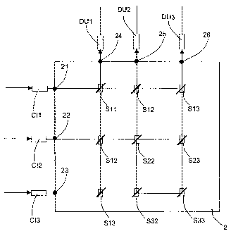
In Figure 2 an optical spatial switching matrix, according to present
invention is shown. In
said figure the matrix is a 3X3 matrix; generally, the present invention
relates to an optical
spatial switching matrix NxM, in which N is the number of input ports (from 1
to M
ports), and M is the number of output ports (from 2 to N ports). Said
switching matrix
comprises preferably a substrate 2 on which a plurality of switching elements
S 11, S 12,
S 13, 521, 522, 523, 532, S31 and S33 are provided. On said substrate at least
one input
port (in figure 1 first 21 second 22 and third 24) and a plurality of output
ports (in figure 1
first 24 second 25 and third 26) are provided.
Preferably, each input port defines a row of said matrix and each said output
port defines a
column of said matrix. Preferably, said switching elements are disposed at the
intersections of said rows and columns. In general, a generic switching
element S;~ is
disposed at the intersection of the row i with the column j.
At input ports, optical signals from external optical fibers or from external
optical
waveguides are collimated using collimators CI1, CI2 and CI3 or lenses or
other
equivalent devices. At output ports, optical signals from the switching matrix
are focused
7
CA 02467668 2004-05-18
WO 03/047304 PCT/EPO1/13996
using focusing devices DU1, DU2 and DU3.
Preferably, said substrate comprises a plurality of waveguides in which the
optical signals
are guided from input ports to switching elements and from switching elements
to output
ports.
Alternatively the optical signals may travel in free-space. The directions of
the optical
beams on the substrate can be chosen from the collimators or lenses CI1, CI2
and CI3. If
on said substrate said waveguides are provided, said substrate is preferably
made of an
optical transmissive material, for example like Lithium Niobate. If the
optical signals
travel in free-space said substrate may be a simple plastic material or a
metallic material,
which has preferably a low thermal expansion coefficient,. like a plastic
material. An
adapted plastic material is a plastic named MACOR°.
Said switching elements are disposed, as above described, like in a matrix
with reference
to the positions of said input ports and output ports. In particular:
~ switching element S 11 connects first input matrix port 21 and first matrix
output
port 24,
~ switching element S 12 connects first input matrix port 21 and second output
' matrix port 25,
~ switching element S 13 connects first input matrix port 21 and third output
matrix
port 26,
~ switching element S21 connects second input matrix port 22 and first output
matrix port 24,
~ switching element S22 connects second input matrix port 22 and second output
matrix port 25,
~ switching element S23 connects second input matrix port 22 and third output
matrix port 26,
~ switching element S31 connects third input matrix port 23 and first output
matrix
port 24,
~ switching element S32 connects third input matrix port 23 and second output
matrix port 25,
8
CA 02467668 2004-05-18
WO 03/047304 PCT/EPO1/13996
~ switching element S33 connects third input matrix port 23 and third output
matrix
port 26.
In figure 3a and 3b a schematical view of a switching element is illustrated.
In particular,
said switching element has preferably a rectangular form and it comprises a
first input face
or port FI1, a second input face or port FI2 that is preferably orthogonal to
said first input
port FI1, a first output face or port FU1 that is in a opposite position with
respect to said
second input port FI2 and a second output face or port FU2 that is preferably
orthogonal to
said first output port FU1.
Said switching element has preferably two operative conditions.
~ An active "on" condition (fig. 3b) in which a second input optical beam OB2
from
said second input face FI2 exits from said second output face FU2..
~ An inactive "off' condition (fig 3a) in which a first input optical beam OBl
from
said first input face FI1 exits from said second output face FU2 and a second
input
optical beam OB2 from said second input face FI2 exits from said first output
face
FU1.
In general, said switching element has at least a condition in which one of
the two input
beams is deviated from its entering direction on the input port and the other
one optical
beam is blocked, and another condition in which both the input optical beams
cross the
switching element without changing the original entering directions.
Said switching element further comprises a switching mechanism that performs
the
transitions between the two conditions. In particular, from an "on" condition
to an "off
condition and vice versa.
The switching mechanism is preferably activated by means of an external
control, for
example an electrical signal, as will be described later. The switching matrix
of present
invention has no movable parts to obtain a switching action; the activation of
a switching
element is obtained by means of acoustic-waves.
The above-described switching matrix operates as follow. In the example of
figure 2 the
matrix is a 3X3 in which from any of the three input ports it is possible to
route an optical
signal to any of the three output ports. For example, for routing an optical
signal from the
9
CA 02467668 2004-05-18
WO 03/047304 PCT/EPO1/13996
first input port 21 to the third output port 26 only the switching element S
13 is activated
into the condition "on". The other entire switching elements may be in the
condition "off'.
Generally, for routing an optical signal form a generic input port i to a
generic output port
j, the switching mechanism and the external control activate into the
condition "on" the
switching element S;~ of the matrix. Each switch element in a predetermined
position of
the matrix, in an activated condition, connects an input port to an output
port, said ports
corresponding respectively to said predetermined position of the matrix.
Said switching element comprises an acousto-optic medium or deflector. An
acousto-optic
medium generally comprises a transparent elasto-optic medium to which an
acousto
transducer is associated, so as to generate optical acoustic waves, which
propagate within
the medium. Said acoustic-optic medium is preferably an isotropic acousto-
optic medium.
More preferably said medium is a Te02 (tellurium oxide) based glass.
For Te02 (tellurium oxide) based glass is intended a glass made of several
chemical
components, of which Te02 is the principal.
Said acousto transducer is for example a piezoelectric transducer plate bonded
to said
acousto-optic medium.
TeOa based glass of an example shows a figure of merit for acousto-optic
effect:
M2 = n6 pa I pv3ac = 23 .9 x 10-ls [s3 / kg],
where n is the refractive index, p is the elastic-optic coefficient, p is the
density of the
material and vA~ is the sound velocity in the medium.
Other examples of acousto-optic glasses are flint glasses and extra dens flint
glasses.
The piezoelectric transducer is preferably a thin plate of quartz (SiO2) or
Lithium niobate
(LiNb03). The transducer launches an acoustic wave along an acoustic wave
vector I~AC,
which is preferably normal to a transducer face.
A radio-frequency signal is applied to the transducer, so that
ICAO = 2w/A = 2~f / vpC,
where A is the spatial period of the acoustic wave, f is the radio frequency.
The presence
of an acoustic wave in the medium causes a portion of an incident optical beam
to be
diffracted.
CA 02467668 2004-05-18
WO 03/047304 PCT/EPO1/13996
Referring to Fig. 5, for efficient acousto optic diffraction to take place,
the momentum
matching condition must be satisfied, i.e.:
KDIF = ZINC +~AC ~
Where KDIF 1S the vector of the diffracted optical beam and K~C is the vector
of the
incident optical beam.
For diffraction in isotropic materials, this relation leads to the Bragg
condition
sin8 = ~, / 2~A = 2f / 2nvAC;
where diffraction angle 0B is defined as in Fig.S, n is the index of
refraction of the
isotropic material, 7~ is the optical wavelength in vacuum.
The diffraction efficiency for the AO effect r~ is defined as the ratio
between the intensity
of the diffracted optical beam h and the intensity of the incident optical
beam Io.
iia
ri=1°(0)=sih locos~B 2W p° '
where L and W represent respectively the length and width of the piezo-
electric
transducer,~,° is the optical wavelength of the incident beam , 9B is
the Bragg angle and Pa
is the acoustic power delivered by the transducer. As MZ increases, the
acoustic power Pa
required to reach a predetermined diffraction efficiency decreases. In turn,
Pa depends on
the electrical power delivered to the transducer. Therefore as M2 increases,
less electrical
power is required to reach the same diffraction efficiency.
Among amorphous materials, a good material is one in which a trade-off is
found among
the following requirements:
elevated M2, low acoustic absorption coefficient, high thermal stability
regarding acoustic
and optical properties, chemical and mechanical stability, elevated optical
transparency
and low chromatic optical dispersion at the wavelength of interest (for
example around
1.500 nm).
In particular, elevated Ma means that MZ is at least one order of magnitude
greater than MZ
for fused Silica (which is 1.51 x 10⁻¹⁵ s3kg 1 at a 7~0= 633nm). This enables
to reach 100%
diffraction efficiency with Pe<lOW at ~,o= l.Sqm, while requiring L to be in
the
centimeter range.
11
CA 02467668 2004-05-18
WO 03/047304 PCT/EPO1/13996
In particular, low optical chromatic dispersion means that the magnitude of
the dispersion
be of the same order of magnitude of silica optical fibers (D = 17 ps/nm Km at
1550nm in
Si02 fibers). In the present case Te02-based glasses typically show a
dispersion in the
range of D= -35 ps/nm Km.
One example of TeOa (tellurium oxide) based glass is the following
composition:
Te02( 62,5% wt.), W03(32.36%wt.), Mg0 (0.55% wt.), Li20 ( 2.42% wt.), TiOa (
2.17%
wt.).
TeOa is the main component and it contributes to high refractive index, low
acoustic
velocity, low acoustic absorption, optical transparency and low chromatic
dispersion;
W03 has been introduced in such a percentage, so as to contribute to an
increase in the
refractive index, without affecting other parameters; MgO is added in such a
percentage in
order to reduce the density of the glass, without increasing the acoustic
velocity; Li20 and
Ti02 help the glass to vetrify; in addition Ti02 increases the refractive
index.
The switching mechanism comprises said acousto-optic transducer which provides
the
commutation between a condition "on" and a condition "off' and vice versa. The
above
cited external control is preferably the radio frequency applied to said
acousto-optic
transducer.
In figure 4 an example of a generic switching element S;~ is shown. In
particular, said
switching element comprises a first prism 31 and a second prism 32, the two
prisms are
bonded each other in a way to from a semi-transparent interface 33.
Advantageously the semi-transparent interface comprises at least a layer of an
optical
conductive medium, for example a thin layer of Au.
Preferably, the two prisms are bonded each other by means of glue. Said glue
is preferably
also an optical conductive medium.
Said semi-transparent interface forms substantially a beam splitter in which
an incident
optical beam is partially transmitted and partially reflected. A splitter
angle 35 is defined
by the geometry of the two prisms and it represents the angle between the
direction of said
transparent interface and the side face of corresponding prism 32 input face
FI2. Such
angle determines the direction of the reflected beam of the semitransparent
interface.
Preferably, said semi-transparent interface comprises at least a layer of
conductive optical
12
CA 02467668 2004-05-18
WO 03/047304 PCT/EPO1/13996
medium. More preferably, said semi-transparent interface comprises at least a
layer of
glue. Preferably, said conductive optical medium and said glue are selected to
form a
dielectric multistrate substantially insensitive to the polarization of an
optical beam. Said
semi-transparent interface partially transmits and partially reflects an
optical beam without
distinguishing between polarizations status. Preferably, the percentage of
transmitted
beam is chosen around 50%. But for special purposes the percentage of
transmitted beam
may be chosen with a different percentage; for example in a matrix, in which
in said
predetermined positions the commutations are more probable, it is advantageous
to choose
a Lower percentage for the transmitted beam, for example 30%.
One example of semitransparent interface insensitive at the polarization can
be composed
of 5 layers, so that an optical beam crosses in the order: first layer of
Ti02, of thickness
tl=308nm and refractive index nl=2.2, second layer of Si, of thickness
tl=310nm and
refractive index n2=3.52,third layer of Ti02, of thickness t3=310nm and
refractive index
n3=2.2,fourth layer of MgF2, of thickness t4=348nm and refractive index
n4=1.38,fifth
layer of TiOa, of thickness t5=348nzn and refractive index n5=2.2.
On the top of the second prism 32 a piezo-electric transducer plate 34 is
provided. When
said transducer is fed with adequate electric current it generates acoustic
waves which
propagates into said second prism into the direction ICAO which is preferably
perpendicular
to the plane of the transducer plate. Said plane of the transducer plate has
preferably a
plane angle 37, which is the angle between the direction of the plane of the
transducer and
parallel to input face FI2. Said plane angle is chosen in a way to form
acoustic waves with
a predetermined direction into the acoustic optic medium as detailed in the
following
As above described said switching element comprises a first input face or port
FIl a
second input face or port FI2 a first output face or port FU1 and a second
output face or
port FU2. Moreover, said switching element comprises a first dark element Ml,
having a
central hole H1 disposed in correspondence of said frst output port and a
second dark
element M2, having a central hole H2, disposed in correspondence of said
second output
port. Said two dark elements transmit an optical beam directed into said holes
and stop an
optical beam directed in the other directions. Said dark elements are
preferably metallic
13
CA 02467668 2004-05-18
WO 03/047304 PCT/EPO1/13996
plates on which black layers are deposited.
Both in presence of an acoustic wave, generated from said piezoelectric plate,
or not, a
first input beam OB 1 entering from the first input port FI1 is transmitted to
the second
output port FU2. A second input beam OB2 entering from the second input port
FI2 is
partially reflected substantially to said second output port and partially
transmitted to said
first output port FU1. In particular, if the transducer is in "off' condition
the reflected
beam R is directed to the second output FU2 with an angulated direction with
respect to
the axis A. Said angle depends from the chosen splitting angle 35. Preferably,
said
splitting angle is chosen in a way to direct said reflected beam R to said
second dark
element not in correspondence of the hole H2. In this way, the reflected
optical beam is
stopped from said second dark element M2.
If the transducer is in "on" condition the acousto-optic diffraction medium is
excited from
the acoustic wave emitted from said piezoelectric plate. This wave causes a
diffraction of
the reflected optical beam and causes a change of the direction of propagation
of the
reflected optical beam. The diffraction optical beam angle changes in
relationship with the
frequency of said acoustic wave. Said frequency is chosen in a way to form a
diffraction
angle 39 which determines a diffracted optical beam R' preferably parallel to
said axis A.
Generally the diffraction angle 39 is chosen in a way to direct the diffracted
optical beam
R' to the hole H2 of said dark element M2. In this way when the switching
element is in
"on" condition an optical beam from said second input port FI2 is directed to
said second
output port.
For example in the matrix of figure 2, to switch a signal from the third
matrix input port
23 to the first matrix output port 24 the switching element S 13 is activated
into the
"on"condition. Said switching element into the "on" condition transmits
partially the
optical beam to said first output port FU1 (see figure 4). Said potential
crosstalk beam is
stopped from the successive switch element S32 which is certainly in an off
condition (to
connect a input matrix port i to a output matrix port j only the Sij element
is activated into
the "on" condition). Generally, the matrix is designed in a way to stop the
crosstalk of a
partially transmitted optical beam of an "on" switch element, from another one
switch
14
CA 02467668 2004-05-18
WO 03/047304 PCT/EPO1/13996
element in the same row, which is certainly in the "off' condition. Each
switching element
in said activated condition has at least one further switching element
inactive in the same
matrix row and in a successive column. No crosstalk arises due ~ to beams
partially
transmitted from a switching element in the last column, i.e. the column
opposite to the
inputs 21-23 in figure 2.
In figure 6a and 6b an example of a switching element is shown. In particular,
in such
example the two prisms are realized in TeOa, the partially-reflecting layer is
made of a
6.45nm-thick Au layer, resulting in a 50% reflection of the s-polarized
component and a
98 % reflection of the p-polarization component of the optical beam. The
dependence on
the polarization is a function of the incidence angle of the beams.
The splitting angle 35 is around 45.5° and the plane angle 37 is around
0.5°. The
frequency of the acoustic wave is chosen around 80 MHz. The transducer 34 is a
thin plate
of quartz (Si Oa).
Said optical switching matrix as above described is designed preferably to use
in an
optical network with multiwavelength signals. For this reason the switching
elements of
invention must be substantially insensitive at the wavelengths; in particular,
the switching
elements of the invention must be substantially insensitive at the wavelength
preferably
into the amplification band of optical amplifiers contained in such network.
In figure 7 a
spectral response of the switching element of figure 6a and 6b is shown. The
optical band
is centered to a wavelength of 1550 nm, which is a typical wavelength value
for a channel
of a multi-wavelength signal of optical networks. In particular, the graph of
figure 7 shows
four curves, which are referred to different length of said transducer of
figures 6a and 6b.
Each curve is referred to a predetermined length of the transducer.
From the curves is has to be noted that the -3dB wavelength band (identified
in figure 7
with the line B) ,which is a typical value of acceptable losses in a network
band, is for
example around 300 nm for a length of L of 10 millimeter. Said band is
sufficient to cover
an entire set of channels of a multi-wavelength signal in a dense
multiwavelength system.