Note : Les descriptions sont présentées dans la langue officielle dans laquelle elles ont été soumises.
CA 02473568 2004-07-15
WO 03/063369 PCT/US03/01613
AN INTEGRATED HIGH-SPEED SERIAL-TO-PARALLEL AND
PARALLEL-TO-SERIAL TRANSCEIVER
TECHNICAL FIELD OF THE INVENTION
This invention relates generally to communication
systems and more particularly to high-speed transceivers
used therein.
BACKGROUND OF THE INVENTION
Communication systems are known to transport large
amounts of data between a plurality of end user devices,
which, for example, include telephones, facsimile machines,
computers, television sets, cellular telephones, personal
digital assistants, et cetera. As is also known, such
communication systems may be local area networks (LAN)
and/or wide area networks (WAN) that are stand-alone
communication systems or interconnected to other local area
networks and/or wide area networks as part of the public
switched telephone network, public switched data network,
integrated service digital network, the Internet, et
cetera. As is further known, communication systems include
a plurality of system equipment to facilitate the
transporting of data. Such system equipment includes, but
is not limited to, routers, switches, bridges, gateways,
protocol converters, frame relays, private branch
exchanges, et cetera.
The transportation of data within communication
systems is governed by one or more standards that ensure
the integrity of data conveyances and fairness of access
for data conveyances. For example, there are a variety of
Ethernet standards that govern serial transmissions within
a communication system at data rates of 10 megabits per
second, 100 megabits per second, 1 gigabit-per-second and
beyond. In accordance with such standards, many system
components and end user devices of a communication system
transport data via serial transmission paths. Internally,
however, the system components and end user devices process
data in a parallel manner. As such, each system component
and end user device includes at least one high-speed
CA 02473568 2004-07-15
WO 03/063369 PCT/US03/01613
transceiver, which includes a high-speed serial-to-parallel
receiver and a high-speed parallel-to-serial transmitter.
As the demand for data throughput increases, so do the
demands on the high-speed transceiver. The increased
throughput demands are pushing some current integrated
circuit manufacturing processes to their operating limits,
where integrated circuit processing limits (e.g., device
parasitics, trace sizes, propagation delays, device sizes,
et cetera) and IC fabrication limits (e.g., IC layout,
1o frequency response of the packaging, frequency response of
bonding wires, et cetera) limit the speed at which a high-
speed transceiver may operate, jitter performance, and/or
noise performance. Such limitations are forcing
transceiver designers to seek alternative implementations.
For instance, some designers are electing to use multiple
serial paths coupled in parallel to transmit data at higher
rates. For example, to obtain a 10 gigabit-per-second
path, four 3.125 gigabit-per-second transceivers are bonded
together to function as a 10 gigabit-per-second
transceiver. The bonding requires that each 3.125 gigabit-
per-second path operate in a known and controlled
relationship with respect to the other paths such that
transceived data can be accurately transmitted and
subsequently reconstructed. As such, additional circuitry
is needed to achieve the bonding and additional buses are
needed to transport the bonded data. As is known, each bus
requires a separate driver to mitigate transmission line
effects of the bus, thus, each additional bus requires an
additional driver, which increases power consumption.
Another alternate high-speed transceiver
implementation is to use multilevel encoding over a single
bus. As is known, multilevel encoding uses various voltage
levels to indicate the value of data currently being
transmitted. For example, four different voltage levels
may be used to represent two bits of data. For accuracy of
transmission, the difference between each voltage level
should be significant enough to readily distinguish them at
the receiving end. This becomes more difficult as the
supply voltages of the integrated circuit decrease with
2
CA 02473568 2011-09-07
74842-48
improvements in integrated circuit fabrication processes. For instance, 0.10
micron
CMOS technology allows integrated circuits to be powered from a supply voltage
of
approximately 1 volt.
A further alternative for transceivers is to use an integrated circuit
technology that inherently provides for greater speeds. For instance,
switching from
a CMOS process to a silicon germanium or gallium arsenide process would allow
integrated circuit transceivers to operate at greater speeds, but at
substantially
increased manufacturing costs. Currently, for most commercial-grade
applications,
including communication systems, such alternate integrated circuit fabrication
processes are too cost prohibitive for wide spread use.
Therefore, a need exists for a high-speed transceiver that operates at
rates, which push the operating limits of the IC fabrication process, meets
desired
jitter performance requirements and noise requirements, does so without
requiring
bonding of multiple transceivers to achieve the desired rate, and does so for
a given
IC fabrication process.
SUMMARY
According to one aspect of the invention, there is provided a high-speed
communications system comprising: a clocking circuit operably coupled to
produce at
least one high frequency clock; a converter module operably coupled to convert
between serial data and parallel data at a rate corresponding to the at least
one high
frequency clock; and compensation operable to at least partially compensate
for at
least one of integrated circuit operational limitations and integrated circuit
fabrication
limitations of at least one of the clocking circuit and the converter module,
wherein
the converter module is a serial to parallel module operably coupled to
convert
inbound serial data into inbound parallel data at a rate corresponding to the
at least
one high frequency clock, wherein the clocking circuit and the compensation
further
comprise: a fine phase detector operably coupled to produce a fine difference
signal
based on a phase difference between the inbound serial data and a fine
feedback
3
CA 02473568 2011-09-07
74842-48
clock that is representative of the at least one high frequency clock; a fine
charge
pump operably coupled to produce a voltage representative of the fine
difference
signal; a coarse phase and frequency detector operably coupled to produce a
coarse
difference signal based on a difference between a reference clock and a coarse
feedback clock that is representative of the at least one high frequency
clock; a
coarse charge pump operably coupled to produce a voltage representative of the
coarse difference signal; a filter operably coupled to filter the voltage
representation
of the coarse difference signal and the voltage representation of the fine
difference
signal to produce a filtered difference representation; a voltage controlled
oscillator
operably coupled to produce an oscillation based on the filtered difference
representation; a post PLL filter operably coupled to amplify and filter the
oscillation
to produce the at least one high frequency clock; and a coarse divider
operably
coupled to produce the coarse feedback clock from the at least one high
frequency
clock.
BRIEF DESCRIPTION OF THE DRAWINGS
Figure 1 illustrates a schematic block diagram of a high-speed
transceiver in accordance with the present invention;
Figure 2 illustrates a schematic block diagram of a serial-to-parallel
module of the transceiver of Figure 1;
Figure 3 illustrates a timing diagram for the serial-to-parallel module of
Figure 2;
Figure 4 illustrates a schematic block diagram of a serial-to-parallel
converter of the serial-to-parallel module of Figure 2;
Figure 5 illustrates a schematic block diagram of a clocking circuit used
in the receiving section of the transceiver of Figure 1;
Figure 6 illustrates a schematic block diagram of a duty cycle distortion
correction module that can be used in the clocking circuit of Figure 5;
3a
CA 02473568 2004-07-15
WO 03/063369 PCT/US03/01613
Figure 7 illustrates a parallel-to-serial module that
can be used in the transceiver of Figure 1;
Figure 8 illustrates a schematic block diagram of a
parallel-to-serial converter that can be used in the
parallel-to-serial module of Figure 7;
Figure 9 illustrates a schematic block diagram of a
clocking circuit that can be used in the transmitter
section of the transceiver of Figure 1;
Figure 10 illustrates a schematic block diagram of a
duty cycle distortion correction module and phase error
correction module that can be used in the clocking circuit
of Figure 9;
Figure 11 illustrates a graph of a voltage controlled
oscillator in accordance with the present invention;
Figure 12 illustrates a schematic block diagram of an
offset module that can be used in the clocking circuit of
Figure 9; and
Figure 13 illustrates a schematic block diagram of an
alternate transceiver in accordance with the present
invention.
DETAILED DESCRIPTION OF A PREFERRED EMBODIMENT
Generally, the present invention provides a
transceiver that includes a receiver section and a
transmitter section. The receiver section includes a
clocking circuit, a serial-to-parallel module, and
compensation. The transmitter section includes a clocking
circuit, parallel-to-serial module, and compensation. The
compensation within the receiver section and transmitter
section compensates for integrated circuit (IC) processing
limits and/or integrated circuit fabrication limits within
the clocking circuits, serial-to-parallel module, and
parallel-to-serial module that would otherwise limit the
speed at which the transceiver could transport data. By
compensating for IC process limits and IC fabrication
limits, a transceiver fabricated using a given integrated
circuit technology can operate at rates that push practical
limits of operation for the given IC technology. As such,
the use of bonding, multilevel encoding, and/or switching
4
CA 02473568 2004-07-15
WO 03/063369 PCT/US03/01613
to different IC fabrication processes can be avoided and
yet still achieve desired operating rates, desired jitter
performance, and/or desired noise performance.
The present invention can be more fully described with
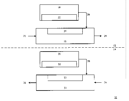
reference to Figures 1 through 13. Figure 1_illustrates a
schematic block diagram of a transceiver 10 that includes a
receiver section 12 and transmitter section 14. The
receiver section 12 includes a receiver clocking circuit
16, serial-to-parallel module 18, and receiver compensation
20. The receiver compensation 20 can be part of the
clocking circuit 16, can be part of the serial-to-parallel
module 18, and/or can be a separate components and/or
modules. The transmitter section 14 includes a transmitter
clocking circuit 28, a parallel-to-serial module 30, and
transmitter compensation 32. The transmitter compensation
32 can be part of the clocking circuit 28, can be part of
the parallel-to-serial module 30, and/or can be separate
components and/or modules.
Both the receiver compensation 20 and transmitter
compensation 32 compensate for integrated circuit (IC)
operational limits and/or IC fabrication limits. Such
integrated circuit operational limits include, but are not
limited to, speed of devices, size of devices, parasitics
of devices, metal track sizes, et cetera. IC fabrication
limits include, but are not limited to, integrated circuit
layout, frequency response of packaging, frequency response
of bonding wires, frequency response of IC pads, component
tolerance variations, et cetera. Such IC operational
limits and/or IC fabrication limits, without compensation,
would, to at least some degree, adversely affect data
throughput of the receiver section 12 and/or the
transmitter section 14.
In operation, the receiver section 12 is operably
coupled to receive inbound serial data 22 via the serial-
to-parallel module 18. The serial-to-parallel module 18,
which will be discussed in greater detail with reference to
Figures 2 and 3, converts the inbound serial data 22 into
inbound parallel data 24 based on a high frequency receiver
clock 26. The receiver clocking circuit 16, which will be
5
CA 02473568 2004-07-15
WO 03/063369 PCT/US03/01613
discussed in greater detail with reference to Figure 5,
generates the high frequency receiver clock 26. The
receiver compensation 20 within the receiver clocking
circuit 16, and/or associated with the receiver clocking
circuit 16, enables the clocking circuit 16 to produce the
high frequency receiver clock 26 at rates that were
previously unobtained using conventional circuit designs.
For example, if the transceiver 10 is implemented utilizing
CMOS integrated circuit processes and conventional circuit
to designs, the speed of the transceiver peaks out near the
3.125 gigabits per second rate due the IC limitations. By
including the compensation 20, the receiver clocking
circuit 10 can produce at least a 12.5 gigabit-per-second
clocking. Similarly, compensation 20 within the serial-to-
parallel module 18 enables the serial-to-parallel module 18
to process the inbound serial data 22 at rates of 12.5
gigabit-per-second.
As one of average skill in the art will appreciate,
transceivers fabricated using different integrated circuit
technologies, such as gallium arsenide or silicon
germanium, will eventually be pushed to their practical
operating limits. Thus, by incorporating compensation in a
similar fashion as disclosed herein, the operation of a
transceiver implemented utilizing such IC technologies can
push the practical limits of operation.
The parallel-to-serial module 30 is operably coupled
to receive outbound parallel data 34 and, based on a high
frequency transmitter clock 38, produces outbound serial
data 36. The transmitter clocking circuit 28 produces the
high frequency transmitter clock 38. Similar to the
compensation within the receiver section, the compensation
32 within the transmitter section 14, enables the clocking
circuit 28 and parallel-to-serial module 30 to operate at
rates that were previously unobtained due to IC operating
limits and/or IC fabrication limits using conventional
circuit implementations. As such, for a CMOS integrated
circuit process, the transmitter clocking circuit 28 can
produce a high frequency clock 38 that operates at 6.125
gigahertz for 12.5 gigabit-per-second operation.
6
CA 02473568 2004-07-15
WO 03/063369 PCT/US03/01613
Accordingly, the parallel-to-serial module can produce
outbound serial data 36 at a 12.5 gigabit-per-second rate.
Figure 2 illustrates a schematic block diagram of the
serial-to-parallel module 18 with compensation 20. The
module 18 with compensation 20 includes an analog front-end
40, an even/odd splitter 42, an even serial-to-parallel
converter 44, an odd serial-to-parallel converter 46, an
optional first-in-first-out memory 48, and an outbound
interface 50. The analog front-end 40 includes an
interface 52, an inductance amplifier 54 and a feed-forward
boost module 56. The inductance amplifier 54 in
combination with the feed-forward boost module 56 provides
compensation for at least some of the integrated circuit
operating limits and/or integrated circuit fabrication
limits. The feed-forward boost module 56 with the
inductance amplifier 54 can provide for an increased
bandwidth with respect to conventional amplifiers. in one
embodiment, the feed-forward boost circuit adequately
boosts the gain of the inductive amplifier to acceptable
levels at frequencies greater than 1 GHz. For example, the
feed-forward boost circuit can boost the gain of the
inductive amplifier to enable operation at 10
Gigabits/second (Gb/sec).
In one embodiment, the feed-forward boost module 56
includes a first boost transistor coupled to receive a
first differential input signal, a second boost transistor
coupled to receive a second differential input signal, and
a boost current source coupled to sources of both the first
and second boost transistors. The drains of the first and
second boost transistors are coupled to first and second
intermediate output nodes of an inductance amplifier
circuit, respectively. In one embodiment, the first and
second intermediate output nodes correspond with ends of
the load resistors of the inductance amplifier.
The AC current inserted by the feed-forward boost
module 56 causes the inductance amplifier 54 to exhibit a
relatively constant gain from DC (0 Hz) up to the resonant
frequency of the entire LC tank circuit formed by the
inductance amplifier 54 and the feed-forward boost module
7
CA 02473568 2004-07-15
WO 03/063369 PCT/US03/01613
56. The signals generated by feed-forward boost module 56
are effectively added to the signals generated by
inductance amplifier circuit 54. As a result, the
frequency response of feed-forward boost module 56 is
effectively added (with some scale factor) to the frequency
response of inductance amplifier circuit 54. Thus, the
feed-forward boost module 56 extends the range of
frequencies at which the inductance amplifier 54 exhibits
an acceptable gain. Moreover, by controlling the sizing of
the first and second boost transistors and the boost AC
current source, the gain amplitude at the resonant
frequency can be controlled. Advantageously, it is not
necessary to use a negative resistance concept to achieve
these results.
In operation, the analog front-end 40 receives the
inbound serial data 22, amplifies, and equalizes it prior
to providing it to the even/odd splitter 42. The even/odd
splitter 42, based on a serial differential clock, which
will be described in greater detail with reference to
Figure 5, produces a serial even data stream 60 and a
serial odd data stream 62. The even and odd data streams
correspond to the sampling of the inbound serial data 22
received from the analog front-end. Referring to Figure 3,
the clock and clock bar illustrate the even and odd
sampling. The inbound serial data 22 is sampled at the
even and odd intervals;of the clock and clock bar. As
such, for each even sample, the even/odd splitter 42
produces a serial data stream 60 at 1/2 the rate of clock and
clock bar. Similarly, the even/odd splitter 42 produce an
odd serial data stream 62 based on the odd sampling
intervals, where the odd serial data stream is 1/2 the rate
of clock and clock bar. In one embodiment, the fine phase
detector 74 (of Figure 5) functions as the even/odd
splitter 42.
Returning back to Figure 2, the even serial-to-
parallel converter 44 receives the even serial data and
converts it into parallel data. For instance, the even
serial-to-parallel converter 44 can convert the serial data
into 8-bit parallel data. The functionality of the even
8
CA 02473568 2004-07-15
WO 03/063369 PCT/US03/01613
serial-to-parallel converter 44 will be discussed in
greater detail with reference to Figure 4.
The odd serial-to-parallel converter 46, at the serial
clock rate, converts the serial odd data into parallel odd
data. For instance, the odd serial-to-parallel converter
46 can convert the serial data into 8-bit parallel data.
The details of the odd serial-to-parallel converter 46 will
also be described with reference to Figure 4.
The FIFO 48 receives the parallel even data and
parallel odd data and stores it at a parallel differential
clock rate. The outbound interface 50 retrieves the even
and odd parallel data to produce the inbound parallel data
24 and transmit to a requesting circuit component of the
device containing the transceiver 10.
Figure 4 illustrates a schematic block diagram of the
even and odd serial-to-parallel converters 44 and 46. Each
converter includes a plurality of high-speed, low-power,
differential D flip-flops 68. A flip-flop 68 in accordance
with one embodiment of the invention has a differential
input stage that incorporates some combinational logic.
This embodiment improves speed performance by reducing or
eliminating the need for separate combinational logic
circuits when the flip-flop 68 is employed in particular
circuit configurations. A flip-flop 68 in accordance with
another embodiment of the invention includes differential
input and output stages, each of which includes a
transistor connected across its differential output
terminals. The transistors are clocked to short the
differential output terminals between expressions of logic
levels, thereby limiting the maximum amount of voltage
swing required to express subsequent logic levels. The
reduction in the maximum voltage swing required reduces the
maximum amount of time required to make logic transitions
at the differential output of flip-flop 68. Reducing the
time required for flip-flop 68 to transition between
different logic levels translates directly into improved
speed performance. Moreover, as compared with prior art
flip-flops, flip-flop 68 can have far fewer transistors,
and can therefore be implemented using less die area.
9
CA 02473568 2004-07-15
WO 03/063369 PCT/US03/01613
These changes also result in significantly reduced power
consumption for a given level of speed performance. The D
flip-flops 68 have a master/slave configuration such that
the 1St D flip-flop receives the even serial data 60 or the
odd serial data 62. On the 1st clocking interval (i.e.,
inputs data on a rise edge, outputs data on a falling edge
of the clock), the 1St D flip-flop produces the output bit
D7. On the next even/odd clock cycle, the top D flip-flop
outputs D6 while the 2nd from the top D flip-flop outputs D7.
Accordingly, the 8-bits (i.e., D7 through Do) propagate
through the plurality of D flip-flops until the even
parallel data 64 or odd parallel data 66 is obtained as
illustrated. Once this data is obtained, it is read into
the FIFO and the next 8 bits are converted from a serial
format to parallel format.
As one of average skill in the art will appreciate,
the D flip-flops can use a differential signaling format
for both input and output signals or a single-ended signal
format.
Figure 5 illustrates a schematic block diagram of the
receiver clock circuit 16 with compensation 20. The clock
circuit 16 with compensation 20 includes two phase locked
loops (PLL): a coarse PLL and a fine PLL. In general, the
coarse PLL establishes the desired frequency for the
clocking circuit and the fine PLL adjusts the phase of the
clock once the frequency is established to align it with
the incoming data, which has a corresponding frequency to
the one generated by the coarse PLL. The coarse PLL
includes crystal 90, coarse phase and frequency detector
78, coarse charge pump 79, filter 80, voltage controlled
oscillator 82, post phase locked loop filter 84, coarse
divider 86, and duty cycle distortion correction module 88.
The fine PLL includes a fine phase detector 74, a fine
charge pump 76, the filter 80, the voltage controlled
oscillator 82, the post phase locked loop filter 84, and
the duty cycle distortion correction module 88. The
clocking circuit can also include an inductance amplifier
70 and feed-forward boost module 72 to provide the incoming
serial data to the fine phase detector 74.
CA 02473568 2004-07-15
WO 03/063369 PCT/US03/01613
To establish the operating frequency for the clocking
circuit, crystal 90, or some other clock source, produces a
reference clock 92 that is provided to the coarse phase and
frequency detector 78. The coarse phase and frequency
detector 78 determines the phase and frequency difference
between the reference clock 92 and a divided representation
of analog clock 94. The coarse divider 86 provides the
divided representation of the analog clock 94 to the coarse
phase and frequency detector 78. Based on the phase and
1o frequency relationship of these signals, the coarse phase
and frequency detector 78 produces a coarse difference
signal. The coarse charge pump 79 receives the coarse
difference signal and produces a voltage representation
thereof and provides it to filter 80.
The filter 80 filters the voltage representation of
the coarse difference signal to produce a filtered
difference representation. The voltage controlled
oscillator 82 receives the filtered signal and produces at
least one clock signal. The voltage controlled oscillator
82 can utilize inductor-capacitor oscillators to produce
the output oscillation. By utilizing inductor-capacitor
oscillators in comparison to ring oscillators, the noise
levels of a voltage controlled oscillator are reduced
thereby compensating for IC limitations of conventional
VCOs using ring oscillators.
As shown, voltage controlled oscillator 82 can produce
a plurality of output clocks including the critical analog
clock 94, an analog clock 96, and a digital clock 98. The
multiple sets of matched clock signals can reduce jitter
and improve jitter tolerance. For example one set of clock
signals can be coupled to a portion of a circuit having
matched loads that are more closely matched than another
set of clock signals that are coupled to another portion of
the circuit. The portion having matched loads can be used
to produce data signals having less jitter, or to process
data signals having a higher degree of jitter, thereby
improving overall jitter performance of the circuit. In
effect, the clock signals driving the matched loads are
isolated from the mismatched load. This isolation
11
CA 02473568 2004-07-15
WO 03/063369 PCT/US03/01613
ultimately allows a circuit to accurately process signals
having a greater degree of jitter.
For at least the critical analog clock 94, a post
phase locked loop filter 84 is included. The post phase
locked loop filter 84 filters and amplifies the oscillation
produced by the voltage controlled oscillator 82 to produce
the critical analog clock 94, and provides compensation.
The post PLL filter 84 reduces the jitter of the PLL output
clock signal by increasing the over Q of the phase locked
loop. In addition, some embodiments of the present
invention also provide amplitude magnification of the PLL
output clock signal.
In accordance with one embodiment of the present
invention, the post PLL filter 84 is an active band pass
filter using complementary input and output signals. The
active band pass filter uses the inherent capacitance on
the output clock lines rather than requiring additional
capacitors. By using the inherent capacitance on the
output clock lines, the active band pass filter provides
amplitude magnification at the desired clock frequency.
The PLL output clock signal is received on the control
terminals of two input transistors. A pair of inductors
coupled in series between a P output terminal and an N
output terminal provides the inductance of the active band
pass filter. A pair of cross-coupled transistors provides
negative Gm and boosts the Q factor of the active band pass
filter. A varacter coupled between the P output terminal
and the N output terminal can be used to tune the active
band pass filter to the desired clock frequency. In a
second embodiment of the present invention, the post PLL
filter 84 includes multiple band pass filters to further
boost the output clock signal.
Once the coarse PLL has established the operating
frequency, the fine PLL becomes active and adjusts the
phase of the operating clock. In operation of the fine
PLL, the inductance amplifier 70 and feed-forward boost
module 72 provide compensation for the inbound serial data
22 which can be received from interface 54. Inductance
amplifier 70 and feed-forward boost module 72 function
12
CA 02473568 2004-07-15
WO 03/063369 PCT/US03/01613
similarly to inductance amplifier 54 and feed-forward boost
module 56, respectively, as described in greater detail
above. In an alternative embodiment, the fine phase
detector 74 can receive the inbound serial data from
inductance amplifier 54 of the analog front end 40 (of
Figure 2) and omit inductance amplifier 70 and feed-forward
boost module 72.
The fine phase detector 74 receives the amplified
serial input data from the inductance amplifier 70 and
to compares it with the critical analog clock 94. Based on a
phase difference between these signals, the fine phase
detector 74 produces a fine difference signal, which is
provided to the fine charge pump 76`. The fine charge pump
76 produces a voltage representation of the fine difference
signal and provides it to the filter 80. The filter 80
filters the voltage representation of the fine difference
signal to produce a filtered difference representation.
The voltage controlled oscillator 82 receives the filtered
signal and produces at least one clock signal.
As illustrated, the clocking circuit 16 with
compensation 20 includes two phase locked loops, one is a
fine phase locked loop based on the data and the other is a
coarse phase locked loop based on a reference clock 92.
Such sequential phased locked loop enables the receiver
section to readily capture the inbound serial data. As one
of average skill in the art will appreciate, the clocking
circuit 16 can use single-ended signals or differential
signals. As one of average skill in the art will further
appreciate, the analog clock 96 and/or digital clock 98 can
also include a post PLL filter 84 and/or duty cycle
distortion correction module 88 to provide the
corresponding filtering, amplifying, and correction
benefits.
The duty cycle distortion correction module 88
receives the critical analog circuit 94 and corrects for
any duty cycle distortion between the positive phase and
negative phase of clock and clock bar. The duty cycle
corrected clock and clock bar are provided to the serial-
to-parallel module 18. Clock and clock bar, as corrected
13
CA 02473568 2011-09-07
74842-48
by the duty cycle distortion correction module 88,
correspond to the serial differential clock referred to in
Figure 2. As one of average skill in the art will
appreciate, the parallel differential clock of Figure 2,
has a rate of 1/8t' of the serial differential clock.
Accordingly, the parallel differential clock can be readily
derived from one of the serial differential' clocks
utilizing a divider, counter, PLL, et cetera. As one of
average skill in the art will further appreciate, an
alternate embodiment of the clocking circuit 16 can have
the duty cycle distortion correction module 88 provide the
feedback to the fine phase detector 74 as opposed to a
direct connection from the post PLL filter 84.
Figure 6 illustrates a schematic block diagram of the
duty cycle distortion correction module 88. In this
embodiment, the duty cycle distortion correction module 88
includes a plurality of inverters 100-106 and correction
blocks 108 and 110. As shown, inverter 100 receives clock
while inverter 104 receives clock bar. The outputs of
inverters 100 and 104 are provided to the serial-to-
parallel converters 44 and 46 of the serial-to-parallel
conversion module 18. In addition, the outputs of
inverters 100 and 104 are provided to inverters 102 and
106, respectively. To compensate for duty cycle variances,
correction blocks 108 and 110 are coupled in parallel with
inverters 102 and 106. Each correction block includes the
circuitry illustrated in the correctibn block 110 coupled
in parallel with inverter 106.
As shown, the correction block 110 includes resistors
116, 118 and 120, capacitors 122 and 124, an operational
amplifier 112 and an inverter 114. In general, resistors
118 and 120 provide a reference voltage to amplifier 112,
which can provide a voltage reference of 'A of the supply
voltage. Resistor 116 in combination with capacitor 122
provides an average voltage representation of the output of
its corresponding inverter. As such, by comparing the
average output of inverter 106 with % the supply voltage, a
difference in duty cycle between the positive phase and
negative phase is obtained. For instance, if the clock is
14
CA 02473568 2004-07-15
WO 03/063369 PCT/US03/01613
operating at exactly 50% duty cycle, the average voltage
produced by resistor 116 and capacitor 122 will match the
voltage produced by the resistive divider 118 and 120. As
such, amplifier 112 will effectively remain off thereby
providing no correction to the input of inverter 106. If,
however, the duty cycle is not 50%, the amplifier 112 will
produce a signal thereby causing inverter 114 to provide
correction to the input of inverter 106. As shown, the
outputs of inverters 102 and 106 are provided to the even
1o and odd splitter 42 of the serial-to-parallel module 18.
Figure 7 illustrates a schematic block diagram of the
parallel-to-serial module 30 with compensation 32. The
module 30 with compensation 32 includes an interface 130, a
FIFO 132, an even parallel-to-serial converter 134, an odd
parallel-to-serial converter 136, an even/odd combiner 138
and a driver 140. The interface 130 can include a
differential input interface having a calibrated input
impedance and a buffer operably coupled to temporarily
store the outbound parallel data 34. In one embodiment,
the interface 130 provides a differential termination
resistor that can be calibrated, for example, for use as an
LVDS termination resistor. The differential termination
resistor is implemented by an on-chip differential
termination structure, which is calibrated against an
external reference resistor. Calibration can be performed
continuously to keep track of changes in temperature and
supply voltage during normal operation of the device.
In one embodiment, a system for calibrating an
adjustable termination resistor is provided. The system
includes an adjustable termination resistor located on a
chip and a reference termination resistor located off the
chip. A bias circuit coupled to the adjustable termination
resistor and the reference termination resistor causes the
same current to flow through the adjustable termination
resistor and the reference termination resistor. The
adjustable termination resistor is initially set to one end
of its range of resistances. For example, the adjustable
termination resistor can initially be set to its lowest
resistance value. A comparator is configured to compare
CA 02473568 2004-07-15
WO 03/063369 PCT/US03/01613
the voltage drop across the adjustable termination resistor
with the voltage drop across the reference termination
resistor. A control circuit is coupled to receive the
comparator output signal. If the comparator output signal
indicates that the voltage drop across the adjustable
termination resistor is greater than the voltage drop
across the reference termination resistor, then the control
circuit stops the calibration operation. The control
circuit then transmits a calibration word representative of
the selected resistance of the adjustable termination
resistor to control other adjustable termination resistors
on the chip. However, if the output signal indicates that
the voltage drop across the reference termination resistor
is greater than the voltage drop across the adjustable
termination resistor, then the control circuit increments
the resistance of the adjustable termination resistor, and
repeats the comparison operation. This process continues
until the comparator determines that the voltage drop
across the adjustable termination resistor is greater than
the voltage drop across the reference termination resistor.
At this time, the control circuit transmits a calibration
word representative of the resistance of the adjustable
termination resistor to control the other adjustable
termination resistors on the device.
In another embodiment, calibration is performed by
each of the differential termination structures on the
chip, thereby increasing the accuracy of the resulting
differential termination resistances. In this embodiment,
the calibration of each of the differential termination
structures is cycled, one at a time, wherein different
differential termination structures are calibrated with the
same external resistor during successive cycles.
In the present invention, power is reduced with
respect to a single-ended termination because there is no
current in the differential termination device, except for
that caused by the differential signal. The present
invention implements a true differential termination for
LVDS or other similar interfaces that fall within the
specifications of the different differential standards. In
16
CA 02473568 2004-07-15
WO 03/063369 PCT/US03/01613
this illustration, the interface 130 receives a 16-bit
representation of the parallel data 34 and provides it to
FIFO 132, which stores it based on a parallel differential
clock. The transmitter clock circuit 28, which will be
described with reference to Figure 9, produces the parallel
differential clock. The data is read from the FIFO 132 as
even parallel data 142 and odd parallel data 144.
The even parallel-to-serial converter 134, which will
be described in greater detail with reference to Figure 8,
receives the even parallel data 142 and produces even
serial data 146 at a rate corresponding to a serial
differential clock. The transmitter clocking circuit 28
produces the serial differential clock. Similarly, the odd
parallel-to-serial converter 136 converts the parallel odd
data 144 into serial odd data 148.
The even/odd combiner 138 receives the even serial
data and odd serial data and produces combined serial data.
In one embodiment, a data combiner employs current sources
and differential current-steering circuits. The current-
steering circuits respond to even/odd pairs of data bits by
producing complementary current signals representing a
differential, serialized version of the pairs of data bits.
In one embodiment, each steering circuit includes a pair of
differential NMOS input transistors having their respective
control terminals (gates) tied to even and odd data
terminals DE, and DOD. Each steering circuit also includes a
pair of differential NMOS input transistors having their
respective control terminals tied to respective
complementary clock terminals. Finally, each steering
circuit includes a pair of PMOS transistors having their
respective control terminals connected to respective data
terminals DEV and DOD. The NMOS and PMOS input transistors
connected to DE, form an inverter that connects between data
terminal DE, and an output terminal via one of the NMOS
transistors connected to the clock terminals. One
embodiment of the invention includes complementary data-
input transistors to expedite the data combiner's response
to changes in input data.
17
CA 02473568 2004-07-15
WO 03/063369 PCT/US03/01613
The driver 140 receives the combined serial data and
produces the outbound serial data 36. The driver 140 can
employ an input stage with an active, LC load. The active
load includes integrated inductors that combine with the,
parasitic gate capacitances of a pair of transistors in a
negative-transconductance (-Gm) booster configuration. The
resulting active load emphasizes a desired frequency,
improving the quality, or "Q," of the input stage, and
consequently of the entire driver. As one of average skill
in the art will appreciate, the signals within the
parallel-to-serial module 30 with compensation 32 can be
single-ended signals or differential signals.
Figure 8 illustrates a schematic block diagram of the
even parallel-to-serial converter 134 and odd parallel-to-
serial converter 136. As shown, the converters 134 or 136
include a plurality of high-speed, low-power differential D
flip-flops 170, which are similar to flip-flops 68,
described above. The plurality of flip-flops is operably
coupled to receive even parallel data 142 or odd parallel
data 144 which, for this illustration, is 8 bits (e.g., D, -
Do). The parallel data is propagated through the plurality
of flip-flops in a serial manner to produce the even serial
data 146 or odd serial data 148. Note that the order
illustrated is most significant bit first. For least
significant bit ordering, the input pattern can be reversed
or the coupling of the plurality of flip-flops can be
reversed.
As one of average skill in the art will appreciate,
the parallel input and serial output can be single-ended
signals or differential signals. In addition, one of
average skill in the art will appreciate the even and odd
parallel data 142 or 144 can be latched into the inputs of
the corresponding D flip-flops via multiplexers, or some
other type of isolation circuit, to provide isolation from
the preceding circuit. One of average skill in the art
will further appreciate, the bottom D flip-flop that is
shown to receive Do as its input, can further include a loop
back from its Q output to its D input to provide a known
18
CA 02473568 2004-07-15
WO 03/063369 PCT/US03/01613
input throughout the propagation of data through the
plurality of flip-flops.
Figure 9 illustrates a schematic block diagram of the
transmitter clocking circuit 28 with compensation 32. The
circuit 28 with compensation 32 includes a crystal 172 or
other clock source, phase and frequency detector 176,
charge pump 178, filter 180, offset module 181, voltage
controlled oscillator 182, post PLL filter 184, divider
186, duty cycle distortion correction module 188, and phase
error correction module 200.
The phase and frequency detector 176 is operably
coupled to determine a difference between phase and
frequency of the reference clock 174 and a divided
representation of the output clock 190. The divider 186
divides an output the VCO 182 to produce the divided
representation of the output clock 190. The charge pump
178 produces a voltage representation of the difference,
which is subsequently filtered by filter 180. The filtered
signal is then provided to the offset module 181, which can
provide a DC offset correction to the filtered signal prior
to providing it as an input to the voltage controlled
oscillator 182. The detail of offset module 181 will be
described in greater detail with reference to Figures 11
and 12.
The voltage controlled oscillator 182 can produce one
or more output oscillations, where at least one is coupled
to a post PLL filter 184. As one of average skill in the
art will appreciate, a post PLL filter 184 can process each
of the output clocks 190, 192 and 194. The voltage
controlled oscillator 182 can utilize inductor/capacitor
oscillators as opposed to ring oscillators to provide
compensation for IC fabrication and/or operation limitation
of ring oscillators. The functionality and operation of
voltage controlled oscillator 182 is similar to the
functionality and operation of voltage controlled
oscillator 82, described in greater detail above.
The post PLL filter 184 filters the clock circuit to
produce a critical analog clock 190. The functionality and
operation of post PLL filter 184 is similar to the
19
CA 02473568 2004-07-15
WO 03/063369 PCT/US03/01613
functionality and operation of post PLL filter 84,
described above. The duty cycle distortion correction
module 188 receives the analog clock 190 and produces
corrected duty cycle clocks therefrom. The phase error
correction module 200 receives the output of duty cycle
distortion correction module 188 and corrects any phase
error between clock and clock bar before providing them to
the parallel-to-serial module 30. As one of average skill
in the art will appreciate, the parallel differential clock
utilized by the parallel-to-serial module 30 can be readily
derived from the serial differential clock produced by the
phase error correction module 200. As one of average skill
in the art will further appreciate, the signals within the
clocking circuit 28 with compensation 32 can be single-
ended signals or differential signals.
Figure 10 illustrates a schematic block diagram of the
duty cycle distortion correction module 188 and the phase
error correction module 200. The duty cycle distortion
correction module 188 includes inverters 210-216 and
correction blocks 108. As shown, the clock and clock bar
signals are inverted via inverters 210 and 214 and provided
to serial-to-parallel converters 134 and 136. Clock and
clock bar are also provided to inverters 212 and 216, which
have corresponding correction blocks 108 coupled in
parallel. As such, the output of the duty cycle distortion
correction module 188 has duty cycle corrected clock and
clock bar signals. However, even though the duty cycles
can be corrected to be 50%, the phase relationship between
clock and clock bar may be skewed due to a differing level
of duty cycle correction between the two signals.
The phase error correction module 200 corrects for any
phase differences between clock and clock bar. The phase
error correction module 200 includes transistors 220, 222,
228, 230 and 232 and a tank circuit, which includes
inductor 224 and capacitor 226. As configured, the phase
error correction module 200 will correct for phase
differences between the inputs received at the gates of
transistor 228 and 230 in accordance to the resonant
frequency of the tank circuit. The resulting phase and
CA 02473568 2004-07-15
WO 03/063369 PCT/US03/01613
duty cycle corrected clock signals are provided to the
combiner 138 of the parallel-to-serial module 30.
Figure 11 illustrates a graph that plots output
frequency versus input voltage of the voltage controlled
oscillator 182. In addition, the graph further illustrates
the functionality of the offset module. As shown, the
graph includes a nominal VCO curve 242. As such, during
normal operation (i.e., without being influenced by the
offset module), the voltage controlled oscillator works in
accordance with the nominal curve. As illustrated, the
nominal curve has an optimal linear region 241, which is
the desired range of operation. When the input voltage to
the voltage controlled oscillator is required to be very
low with respect to the output capabilities of the charge
pump, or is very high approaching VDD, the linearity of the
voltage controlled oscillator and/or phase locked loop may
be affected. Therefore, it is desirable to keep the input
voltage within the optimal linear region 241.
As integrated circuit processes are enabling
integrated circuits to be powered by lower and lower
voltages, the input voltage to achieve the desired output
voltage may approach the supply voltage (e.g., VDD) or
return voltage (e.g., Vs). To obtain optimal VCO
operation, the offset module 181 offsets the output of the
charge pump to VCO curve to compensate for limited supply
voltage headroom. For example, if the input voltage is
large (i.e., near the top of the optimal linear range 241),
the offset module provides an offset (as indicated by the
left pointing arrow) such that the curve is shifted as
shown in curve 244. Conversely, if the desired frequency
is produced at a low input voltage near the bottom of the
optimal linear range 241, the offset module provides an
offset (as indicated by the right pointing arrow) such that
curve 246 is produced. In effect, the offset module 181
allows the VCO to operate where it needs, while allowing
the charge pump to operate where it needs to.
Figure 12 illustrates a schematic block diagram of an
embodiment of offset module 181. The offset module 181
includes an amplifier 250, programmable gain network 254,
21
CA 02473568 2011-09-07
.74842-48
logic 256, output-buffer 252, comparator network 258 and
divider network 260. In nominal operation, (i.e., where no
offset is desired) amplifier 250 will have a gain of 1. As
such, signals received at the input from the filter will be
5, provided as is to the voltage controlled oscillator via the
output buffer 252. If, however, the input is sensed to be
at a level where offset would improve performance, the
comparator network 258, by comparing the input voltage with
the divider network 260, causes the logic 256 to change the
lo gain of the programmable gain network 254. As such, in the
illustration shown, the offset module 181 can produce an
output representation of the input signal ranging from
0.8VV to 1.25Vn,.
As one of average skill in the art will appreciate,
15 the number of steps in changing the gain can be more or
less than the number shown and the switches of the gain
network can be transistors, gates, et cetera. in addition,
one of average skill in the art will appreciate, other
embodiments for producing the programmable gain network
20 254, logic 256 and corresponding inputs to the logic 256
can be readily derived based on the desired functionality
of the offset module 181 and the description provided
herein.
An alternate embodiment of the offset module 181
25 includes a DC voltage setting module and a varactor within
an LC oscillator of the VCO. The varactor, which behaves
as a voltage dependent capacitor, is coupled in series with
AC coupling capacitors that each has a substantially
greater capacitance value than the varactor. The series
30 coupled capacitors, including the varactor, is coupled in
parallel with an inductor to form an LC oscillator of the
VCO. The DC voltage setting module is operably coupled to
the varactor to establish the capacitance of the varactor
and to establish the operating level of the input voltage
35 to the VCO. As such, by varying the signal produced by the
DC voltage setting module, the input voltage level to the
VCO can be varied, thus achieving the desired offset.
Figure 13 illustrates an alternate embodiment of a
transceiver 275 that includes serial-to-parallel module 18,
22
CA 02473568 2004-07-15
WO 03/063369 PCT/US03/01613
parallel-to-serial module 30, clocking circuit 270, and
compensation 272, 274 and 278. The compensation 272, 274
and 278 compensate for integrated circuit operational
limitations and/or integrated circuit fabrication
limitations of the serial-to-parallel module 18, the
clocking circuit 270, and/or the parallel-to-serial module
30.
In operation, the clocking circuit 270 and
corresponding compensation 278 can be implemented as one of
1o the clocking circuits illustrated in Figures 5 or 9, a
portion thereof, and/or a combination thereof to produce at
least one high frequency clock 276. The at least one high
frequency clock 276 is provided to both the serial-to-
parallel module 18 and the parallel-to-serial module 30.
The serial-to-parallel module 18 receives inbound
serial data 22 and produces inbound parallel data 24
therefrom. The implementation of the serial-to-parallel
module 18 with corresponding compensation 272 can be as
described with reference to Figure 2. _
The parallel-to-serial module 30 receives outbound
parallel data 34 and produces outbound serial data 36
therefrom. An embodiment of the parallel-to-serial module
and corresponding compensation 274 can be as illustrated
and described with reference to Figure 7.
25 The preceding discussion has presented a high-speed
transceiver that pushes the operating limits of integrated
circuits. By providing IC limitation compensation, speeds
previously unrealized for transceivers are obtained. As
one of average skill in the art will appreciate, other
30 embodiments can be derived from the teachings of the
present invention without deviating from the scope of the
claims.
23