Note : Les descriptions sont présentées dans la langue officielle dans laquelle elles ont été soumises.
CA 02475372 2004-08-05
WO 03/067587 PCT/IB03/00221
Rewritable optical storage medium and use of such medium
The invention relates to a rewritable optical storage medium for erasable high
data rate recording by means of a focused laser-light beam, said medium
comprising:
a substrate; and a stack of layers on the substrate; which stack includes: a
first
dielectric layer; a recording layer of a phase-change material comprising an
alloy consisting
of Ge, Sb and Te; a second dielectric layer; and a metal reflective layer.
The invention also relates to the use of such an optical recording medium in
high data rate applications.
An embodiment of an optical data storage medimn of the type mentioned in
the opening paragraph is known from United States patent US 5,935,672 filed by
Applicants.
An optical data storage medium based on the phase-change principle is
attractive, because it combines the possibilities of direct overwrite (DOW)
and high storage
density with easy compatibility with read-only optical data storage systems.
Data storage, in
this context, includes digital video-, digital audio- and software-data
storage. Phase-change
optical recording involves the formation of submicrometer-sized amorphous
recording marks
in a crystalline recording layer using a focused relatively high power laser-
light beam. During
recording of information, the medium is moved with respect to the focused
laser-light beam
that is modulated in accordance with the information to be recorded. Marks are
formed when
the high power laser-light beam melts the crystalline recording layer. When
the laser-light
beam is switched off and/or subsequently moved relatively to the recording
layer, quenching
of the molten marks takes place in the recording layer, leaving an amorphous
information
mark in the exposed areas of the recording layer that remains crystalline in
the unexposed
areas. Erasure of written amorphous marks is realized by recrystallization
through heating
with the same laser at a lower power level, without melting the recording
layer. The
amorphous marks represent the data bits, which can be read, e.g. via the
substrate, by a
relatively low-power focused laser-light beam. Reflection differences of the
amorphous
marks with respect to the crystalline recording layer bring about a modulated
laser-light beam
CA 02475372 2004-08-05
WO 03/067587 PCT/IB03/00221
2
which is subsequently converted by a detector into a modulated photocurrent in
accordance
with the recorded information.
One of the most important requirements in phase-change optical recording is a
high data rate, which means that data can be written and rewritten in the
medium with a user
data rate of at least 25 Mbits/s. Such a high data rate requires the recording
layer to have a
high crystallization speed, i.e. a short crystallization time, during DOW. To
ensure that
previously recorded amorphous marks can be recrystallized during DOW, the
recording layer
must have a proper crystallization speed to match the velocity of the medium
relative to the
laser-light beam. If the crystallization speed is not high enough the
amorphous marks from
the previous recording, representing old data, cannot be completely erased,
meaning
recrystallized, during DOW. This causes a high noise level. A high
crystallization speed is
particularly required in high-density recording and high data rate optical
recording media,
such as in disk-shaped CD-RW high speed, DVD-RW, DVD+RW, DVD-RAM, DVR-red and
blue which respectively are abbreviations of the known Compact Disk and the
new
generation high density Digital Versatile or Video Disk+RW and -RAM, where RW
and
RAM refer to the rewritability of such disks, and Digital Video Recording
optical storage
disks, where red and blue refer to the used laser wavelength. For these new
disks, the
complete erasure time (CET) has to be lower than 40 ns. CET is defined as the
minimum
duration of an erasing pulse for complete crystallization of a written
amorphous mark in a
crystalline environment. The CET is measured with a static tester. For DVD+RW,
which has
a 4.7 GB recording density per 120 mm disk, a user data-bit rate of 26 Mbits/s
is needed, and
for DVR-blue said rate is 35 Mbits/s. For high speed versions of DVD+RW and
DVR-blue
data rates of 50 Mbits/s and higher are required. The data rate for
Audio/Video (AV)-
applications is determined by the AV information stream but for computer-data
applications
no restrictions in data rate apply, i.e. the larger the better. Each of these
data bit rates can be
translated to a maximum CET which is influenced by several parameters, e.g.
thermal design
of the recording stacks and the recording layer materials used.
The known medium of the phase-change type comprises a disk-shaped
substrate carrying a stack of layers consisting, in succession, of a first
dielectric layer, a
recording layer of a phase-change Ge-Sb-Te alloy, a second dielectric layer
and a metal
reflective layer. Such a stack of layers can be referred to as an IPIM
structure, wherein M
represents a reflective metal layer, I represents a dielectric layer and P
represents a phase-
change recording layer. Said patent discloses a compound GeSOXSb4o-4oXTeso-ioX
~ w~ch
formula 0.166 ~ <_0.444. Stoichiometric Ge-Sb-Te materials falling within the
mentioned
CA 02475372 2004-08-05
WO 03/067587 PCT/IB03/00221
3
range, e.g. Ge2SbZTeS, are used as the recording layer for e.g. DVD-RAM disks.
These
stoichiometric compositions have a nucleation-dominated crystallization
process. It means
that the erasure of a written amorphous mark occurs by nucleation in the mark
and
subsequent growth. According to said patent the CET of said Ge-Sb-Te layer
decreases by
increasing its thickness up to 25 nm and then tends to become a constant upon
further
increase of the layer thickness at a value of about 50 - 60 ns. A thickness
range between 25
and 35 nm has been claimed for use in high data rate recording. When the
thickness of the
recording layer becomes smaller than 25 ns the CET increases to values above
80 ns.
The known recording medium shows a minimum CET of its recording layer of
about 50 - 60 ns and the CET tends to increase going to smaller recording
layer thicknesses.
For multi recording layer applications it is desirable that the recording
layer, which is closest
to the recording/reading laser-light beam, has a relatively high optical
transmission in order
to allow writing and reading in further recording layers. A relatively high
optical
transmission of the recording layer can only be achieved when its thickness is
lower than 25
nm. However, at recording layer thicknesses of 25 nm or less the CET of the
known medium
increases to values which are less suitable for high data rate recording.
It is an object of the invention to provide a rewritable optical storage
medimn
of the kind described in the opening paragraph, having a recording layer with
a thickness of
lower than 25 nm and a CET of maximum 40 ns, making it suitable for high data
rate
recording.
This object is achieved in accordance with the invention by an optical storage
medium as described in the opening paragraph, which is characterized in that
the alloy has a
composition defined by the formula GeXSbyTeZ in atomic percentages, where 0 <
x < 15,
50 < y < 80, 10 < z < 30 and x + y + z = 100; and the recording layer has a
thickness selected
from the range of 7 to 18 nm. These materials have a growth-dominated
crystallization
process. It means that mark erasure occurs by direct growth from the boundary
between the
written amorphous mark and crystalline background. Nucleation within the
written
amorphous mark does not occur before this growth is finished. Surprisingly,
the CET of these
materials first decreases rapidly with increasing the layer thickness and then
increases again
upon further increasing layer thickness. The CET becomes shorter than 40 ns
when the
recording layer has a thickness selected from the range of 7 to 18 nm. The
thickness
dependence of the CET of the claimed Ge-Sb-Te compositions may be understood
as
CA 02475372 2004-08-05
WO 03/067587 PCT/IB03/00221
4
follows. The strong initial decrease of the CET with the increase of the phase-
change
recording layer thickness is a result of competition between the contributions
of the interface
material and the bulk material. When the layer is relatively thin, the volume
fraction of the
material located at the interface is large, which is often structurally very
different from its
bulk form, e.g. has more defects. With the increase of layer thickness, the
fraction of the
material that is in bulk form will increase, and above a certain thickness the
behavior of the
material will be governed by the bulk form. Apparently, the bulk materials
have a more
favorable growth speed than the interface materials.
Upon further increase of the phase change layer thickness the increase of the
CET may be caused by the volume increase of the material. The crystallization
process of the
claimed Ge-Sb-Te layer is growth-dominated. The volume of the material to be
crystallized
becomes important. The size of the crystallites is typically 10 nm. When the
layer is thin, a
two-dimensional growth is needed, which needs a shorter time. When the layer
becomes
thicker, a three-dimensional growth is required, and naturally a longer time
is needed.
W a favorable embodiment of the optical storage medium according to the
invention, the recording layer has a thickness selected from the range of 8.5
to 13 nm. In this
range the CET is lower than 35 ns which enables even higher data rates.
In another favorable embodiment of the optical storage medium according to
the invention the second dielectric layer has a thickness of 20 to 40 nm. An
optimum
thickness range for the second dielectric layer, i.e. the layer between the
recording layer and
the metal reflective layer, is found between 15 and 50 nm, preferably between
20 and 40 rim.
When this layer is too thin, the thermal insulation between the recording
layer and the metal
reflective layer is adversely affected. As a result, the cooling rate of the
recording layer is
increased, which leads to slow crystallization process and a poor cyclability.
The cooling rate
will be decreased by increasing the thickness of the second dielectric layer.
The CET is not
sensitive to the thickness of the metal reflective layer. Its thickness may
e.g. be in the range
from 20 to 200 nm. But the cyclability is adversely affected when the metal
reflective layer is
thinner than 60 nm, because the cooling rate is too slow. When the metal
reflective layer is
160 nm or thicker, the cyclability deteriorates further, and the recording and
erasing power
must be high because of the increased thermal conduction. Preferably the
thickness of the
metal reflective layer is between 80 and 120 nm.
In yet another favorable embodiment of the optical storage medium according
to the invention the first dielectric layer has a thickness of 70 to 500 nm.
When the first
dielectric layer has a thickness lower than 70 nm the cyclability of the
medium is adversely
CA 02475372 2004-08-05
WO 03/067587 PCT/IB03/00221
affected. Thicknesses larger than 500 nm may cause stresses in the layer and
are more
expensive to deposit.
In a special embodiment of the optical storage medium according to the
invention a further recording layer is present in the stack having the same
composition as the
5 (first) recording layer. The fuxther recording may be sandwiched between
dielectric layers
similar to the dielectric layers of the (first) recording layer. Further
auxiliary layers may be
present. In a so-called mufti recording stack medium two or more recording
layers are
present separated from each other by intermediate layers at a distance larger
than the depth of
focus of the laser-light beam. Sometimes mufti-stack designs are represented
by Ln in which
n denotes 0 or a positive integer number. The first stack through which the
laser-light beam
enters is called Lo, while each deeper stack is represented by Ll.. L". Deeper
is to be
understood in terms of the direction of the incoming laser-light beam. During
writing onto
and reading from such a medium the laser-light beam is focused onto the
recording layer of
one of the Ln stacks. E.g. in the case of a double stack medium with a Lo and
a Ll stack, in
order to have sufficient write energy and reading signal the Lo-stack must be
sufficiently
transparent. This is only possible when the recording layer of the Lo-stack
has a relatively
low thickness of 25 nm or thinner. The Ll stack, being the deepest stack, may
have a thicker
recording layer because it does not necessarily have to be optically
transparent. According to
the invention a low CET is combined with a low recording layer thickness which
makes the
recording layer according to the invention suitable for use in a mufti
recording stack medium.
The first and second dielectric layers may be made of a mixture of ZnS and
Si02, e.g. (ZnS)8o(SiOz)ao. Alternatives are, e.g. Si02, Ti02, ZnS, A1N and
Ta205. Preferably
the dielectric layer comprises a carbide, like SiC, WC, TaC, ZrC or TiC. These
materials give
a higher crystallization speed and better cyclability than ZnS-Si02 mixture.
For the metal reflective layer, metals such as Al, Ti, Au, Ni, Cu, Ag, Cr, Mo,
W, and Ta and alloys of these metals, can be used.
The substrate of the data storage medium is at least transparent for the laser
wavelength, and is made, for example, of polycarbonate, polymethyl
methacrylate (PMMA),
amorphous polyolefin or glass. Transparency of the substrate is only required
when the laser-
light beam enters the recording stacks via the entrance face of the substrate.
In a typical
example, the substrate is disk-shaped and has a diameter of 120 mm and a
thickness of 0.1,
0.6 or 1.2 mm. The substrate may be opaque when the laser-light beam enters
the stack via
the side opposite from the side of the substrate. In the latter case the metal
reflective layer of
CA 02475372 2004-08-05
WO 03/067587 PCT/IB03/00221
6
the stack is adjacent the substrate. This is also referred to as an inversed
stack. An inversed
stack is e.g. used in the DVR disk.
The surface of the disk-shaped substrate on the side of the recording stacks
is,
preferably, provided with a servotrack, which can be scanned optically. This
servotrack is
often constituted by a spiral-shaped groove and is formed in the substrate by
means of a
mould during injection molding or pressing. These grooves can be alternatively
formed in a
replication process in the synthetic resin of the spacer layer, for example, a
W light-curable
acrylate
Optionally, the outermost layer of the stack is screened from the environment
by means of a protective layer of, for example, IJV light-cured
poly(meth)acrylate. The
protective layer must be of good optical quality, i.e. substantially free from
optical
aberrations and substantially uniform in thickness, when the laser-light
enters the recording
stacks via the protective layer. In tlus case, the protective layer is
tra~.isparent to the laser-light
and is also called cover layer. For DVR disks this cover layer has a thickness
of 0.1 mm.
Recording and erasing data in the recording layers of the recording stacks may
be achieved by using a short-wavelength laser, e.g. with a wavelength of 660
nm or shorter
(red to blue).
Both the metal reflective layer, and the dielectric layers can be provided by
evaporation or sputtering.
The phase-change recording layer can be applied to the substrate by vacuum
deposition. Known vacuum deposition processes are evaporation (E-beam
evaporation,
resistant heat evaporation from a crucible), sputtering, low pressure Chemical
Vapor
Deposition (CVD), Ion Plating, Ion Beam Assisted Evaporation, Plasma enhanced
CVD.
Normal thermal CVD processes are not applicable because of too high reaction
temperature.
The layer thus deposited is amorphous and exhibits a low reflection. In order
to constitute a
suitable recording layer having a high reflection, this layer must first be
completely
crystallized, which is commonly referred to as initialization. For this
purpose, the recording
layer can be heated in a furnace to a temperature above the crystallization
temperature of the
Ge-Sb-Te alloy, e.g. 180°C. A synthetic resin substrate, such as
polycarbonate, can
alternatively be heated by a special laser-light beam of sufficient power.
This can be realized,
e.g. in a special recorder, in which case the special laser-light beam scans
the moving
recording layer. The amorphous layer is then locally heated to the temperature
required for
crystallizing the layer, without the substrate being subjected to a
disadvantageous heat load.
CA 02475372 2004-08-05
WO 03/067587 PCT/IB03/00221
7
High-density recording and erasing can be achieved by using a short-
wavelength laser, e.g. with a wavelength of 660 nm or shorter (red to blue).
The invention will be elucidated in greater detail by means of exemplary
embodiments and with reference to the accompanying drawings, in which
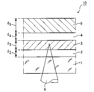
Fig. 1 shows a schematic cross-sectional view of an optical storage medium in
accordance with the invention,
Fig. 2 shows the relation between CET (in ns) and the thickness d3 (in nm) of
the recording layer for Ge7Sb76.4Te1s.~ material.
Example.
In Fig 1 shows a part of a cross-section of a rewritable optical storage
medium
10 for erasable high-speed recording in accordance with the invention.
Recording and
reading is performed by means of a laser-light beam 6. The medium 10 has a
substrate 1
made of PC having a diameter of 120 mm and a thickness of 0.6 mm. An IPIM
stack of
layers is present on the substrate including a first dielectric layer 2 of
(ZnS)8o(SiOz)zo with a
thickness dz=70 nm, a recording layer 3 of a phase-change material with the
composition
Ge7Sb76.4Te1s.6 with a thickness d3, and a second dielectric layer 4 of
(ZnS)$o(Si~z)zo with a
thickness d4= 20 nm and a metal reflective layer 5 of Al with a thickness
ds=100 nm. The
recording layer 6 having a thickness d3 is varied between 4 and 30 nm. Results
of the effect
of this variation are shown in Fig.2.
The phase-change recording layer 3 is applied to the substrate by vapor
depositing or sputtering of a suitable target. The layer 3 thus deposited is
amorphous and is
initialized, i.e. crystallized, in a special recorder, as described earlier.
The layers 2, 4 and 5
are also provided by sputtering.
The laser-light beam 6 for recording, reproducing and erasing of information
enters the recording layer 3 via the substrate 1. The amorphous marks are
written with a
single laser pulse of power PW = 1.25 Pm (Pm melting threshold power) and
duration 100 ns.
The erase power is PW/2. Note that alternative embodiments are possible in
which the
substrate 1 is present adjacent the metal reflective layer 5 while the laser-
light beam 6 still
enters the recording layer 3 through layer 2. In this case an optional
optically transparent
cover layer of e.g. 0.1 mm may be present adjacent dielectric layer 2.
CA 02475372 2004-08-05
WO 03/067587 PCT/IB03/00221
8
In Fig. 2 the dependence of the CET in ns on the thickness d3 in nm of the
phase-change recording layer 3 for the compound Ge~Sb76_4Tels.s is shown. From
curve 11 of
Figure 2 it is clear that the CET decreases rapidly by increasing d3 up to
about 10 nm, and it
tends to increase slowly and saturate at a low value of about 47 ns upon
further increase of
d3.
It should be noted that the above-mentioned embodiment illustrates rather than
limits the invention, and that those skilled in the art will be able to design
many alternative
embodiments without departing from the scope of the appended claims. In the
claims, any
reference signs placed between parentheses shall not be construed as limiting
the claim. The
word "comprising" does not exclude the presence of elements or steps other
than those listed
in a claim. The word "a" or "an" preceding an element does not exclude the
presence of a
plurality of such elements. The mere fact that certain measures are recited in
mutually
different dependent claims does not indicate that a combination of these
measures cannot be
used to advantage.
According to the invention an erasable optical storage medium is provided,
which is suitable for direct overwrite and high data rate recording, such as
DVD+RW and
rewritable DVR, having a relatively thin phase change type recording layer
with a possible
data rate of at least 25 Mb/s.