Note : Les descriptions sont présentées dans la langue officielle dans laquelle elles ont été soumises.
CA 02475520 2004-07-22
SPECIFICATION
TITLE OF THE INVENTION
DRIVER CIRCUIT
BACKGROUND OF THE INVENTION
Field of the Invention
A driver circuit of the present invention relates to an output driver
circuit the output signal of which is connected to an input of a device in the
next stage via a member having a parasitic inductance such as a wire and
performs current drive or voltage drive and, more specifically, to a drive
circuit in which the effect of the parasitic inductance that varies according
to applied material and packaging can be reduced, and good output
matching and wide band characteristics can be maintained.
Description of the Related Art
Recently, as the Internet becomes widespread, transmission rates
required for an IC for optical communication is ever-increasing into 10 Gb/s
to 40 Gb/s. In order to realize the speeding up of the IC, it is necessary
that high speed response characteristics of transistors constituting the IC
are improved, and characteristic deterioration such as band limiting at the
time of mounting is suppressed. Especially, in an LC circuit constituted by
a parasitic capacitance (a pad capacitance, an output capacitance of a
transistor, etc.) of the output end of an IC or a parasitic inductance such as
a
wire connected to the input of a device in the next stage, band limiting and
output mismatching becomes a factor of characteristic deterioration.
1
CA 02475520 2004-07-22
In order to solve the problem, conventionally, a filter as shown in Fig.
19.6.2 of "40Gb/s 2:1 Multiplexer and 1=2 Demultiplexer in 120nm CMOS,"
ISCCC Digest of Technical Papers, pp. 344-345, 2003 is constituted at the
output end of the IC.
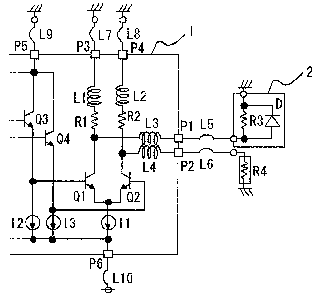
A conventional configuration example of a driver circuit having the
filter of the above document is shown in Fig. 11. In Fig. 11, an IC chip 1 as
the driver circuit has a pair of differential transistors Qi, Q2, a constant
current source I1 connected between emitter terminals of the pair of
differential transistors Q 1, Q2 and a negative voltage terminal within the
IC for setting current driving in the pair of differential transistors Q l,
Q2,
emitter follower transistors Q3, Q4 for inputting output signals drawn from
the emitter terminals of themselves to base terminals of the pair of
differential transistors Q 1, Q2, constant current sources 12, 13 connected
between the emitter terminals of the emitter follower transistors Q3, Q4
and the negative voltage terminals within the IC, respectively, for setting
current flowing in the emitter follower transistors Q3, Q4, terminating
resistors R1, R2 for IC internal matching connected to collector output
terminals of the pair of differential transistors Q 1, Q2, inductors L1, L2
connected between the collector outputs of the pair of differential
transistors
Q1, Q2 and a positive voltage terminal within the IC via the terminating
resistors Rl, R2, respectively, bonding pads P1, P2 respectively provided on
differential output parts of the IC chip 1, inductors L3, L4 inserted between
the collector output terminals of the pair of differential transistors Q1, Q2
and the bonding pads Pl, P2, respectively, a bonding pad P5 connected to
the positive voltage within the IC, and a bonding pad P6 connected to the
2
CA 02475520 2004-07-22
negative voltage within the IC.
A wire L9 connects the pad P5 and a positive voltage source on the
mounting substrate, a wire L10 connects the pad P5 and the negative
voltage source on the mounting substrate.
Alight output part 2 driven by the IC chip 1 includes an optical
modulator D and a resistor R3 connected in parallel with the modulator, and
an anode of the optical modulator D is connected to the pad P5 through a
wire L5 and a cathode of the optical modulator D is connected to a positive
voltage source. Further, a terminating resistor R4 is connected between
the pad P2 and the positive voltage source via a wire L6.
In the driver circuit in Fig. 11, the wideband characteristics of the
IC are realized by the effects of the inductors L1, L2 serially connected to
the terminating resistors Rl, R2, respectively, for inductor peaking, and the
inductors L3, L4 connecting the respective collector outputs of the pair of
differential transistors Ql, Q2 and the IC output pads P1, P2. Further, the
filter is constituted by the on-chip inductors (L1 to L4), output capacitances
of the pair of differential transistors Q1, Q2, the pad capacitances of P1,
P2,
and the bonding wires L5, L6 and, by optimizing the L value, the cutoff
frequency of the filter itself can be made sufficiently higher so that the
cutoff frequency may not become a factor of the band limiting of the entire
IC. Further, characteristic impedance of the filter can be set to desired
values by the optimization of the L value. The improvement in bands and
good output matching characteristics have been realized by the output
circuit having such a filter.
Moreover, in "20Gb/s transimpedance preamplifier and modulator
3
CA 02475520 2004-07-22
driver in SiGe bipolar technology", IEE Electron Lett. Vol. 32, No. 13, pp.
1136 to 1137, 19, June, 1997), rising/falling time of an output waveform is
improved by inserting a bonding wire in serial with a terminating resistor.
In the driver circuit having the filter in the conventional form,
inductances of the wires L5, L6 are required to be specified at the time of
design. However, in a driver for driving a laser diode or an optical
modulator, for example, there are some cases where used packages are
different according to their application, the driver is bare chip mounted for
miniaturization of a module and a transmission unit, or an IC and an
optical element are spaced and connected by a long wire by intention so that
the effect of heat generation of the IC may not adversely affect the
characteristics of the optical element. On this account, it has become
difficult to uniquely determine inductances of the wires L5, L6 in advance.
Therefore, despite the fact that the h.lter is provided, there has been
a problem that band deterioration and output mismatching can not be
suppressed sufficiently due to the effect of inductances that vary according
to packaging. Furthermore, in the case where the filter is constituted in a
driver circuit having the conventional form in whicli the signal from the
emitter follower is amplified, there has been a problem that, as described in
detail below, the characteristics of the emitter follower affect the output
impedance of the driver circuit and output capacitances of the pair of
differential transistors Q1, Q2 do not appear to be ideal capacitances;
thereby, good filter characteristics can not be obtairied.
The effect on the output impedance of the differential amplifier
when output impedance of the differential amplifier, the output impedance
4
CA 02475520 2004-07-22
of the emitter follower, and the emitter fo]lower are connected to the input
will be described below. Basic equivalent circuits of the differential
amplifier are shown in Figs. 12a to 12c. Fig. 12a is a circuit diagram of the
differential amplifier including the transistors Q l, Q2 and the terminating
resistors R1, R2. When a differential signal is input to the differential
amplifier in Fig. 12a, the common emitter point becomes a virtual grounded
point, and the differential amplifier can be replaced by a single-ended
equivalent circuit. Therefore, the small-signal equivalent circuit is shown
by Fig. 12b (see "Analysis and Design of Analog Integrated Circuits -Fourth
Edition-").
In Fig. 12b, RS denotes an output impedance of an input signal
source, rb denotes a base resistor, rg denotes an input resistor, Cic denotes
a
base-emitter capacitance, Cg denotes a base-collector capacitance, gm
denotes a transconductance, RL denotes a resistance value of the
terminating resistor R1 or R2, vi denotes a voltage of the signal source, v1
denotes a voltage applied to both ends of the resistor r7r, and vo denotes an
output voltage drawn from both ends of the resistor RL.
Fig. 12c shows an output impedance equivalent circuit obtained
from the equivalent circuit in Fig. 12b. As shown in Fig. 12c, the output
impedance of the transistor Q 1 or Q2 is represented by two CR series
circuits connected in parallel. Of these two CR series circuits, because the
magnitude of a capacitance proportional to gm varies according to the
condition of the collector current of the transistor Q'1 or Q2, when the
collector current is large, the impedance of the CR circuit constituted by the
capacitance proportional to gm becomes small and dominant; however,
CA 02475520 2004-07-22
because, in a condition in which the transistor is off, the capacitance
proportional to gm becomes smaller than C as gm becomes smaller, in turn,
the impedance of the CR circuit constituted by C becomes dominant.
Consequently, the output capacitance of the transistor Q1 or Q2 is estimated
as C of the either dominant CR circuit.
Fig. 13 shows S22 (a voltage reflection coefficient indicative of the
relationship between the input voltage and the reflection voltage) as S
parameter of the differential amplifier in a condition in which the collector
current is relatively larger plotted on a Smith chart.. It is also seen from
Fig. 13 that the output impedance of the differential amplifier is
represented by a parallel circuit of the load resistor RL and the CR series
circuit, that is, the output impedance of the transistor is represented by the
CR series circuit. Therefore, in the case of constituting the filter, the
filter
is designed in consideration of the value of C in the CR series circuit
estimated from the Smith chart.
Next, the output impedance of the emitter follower wiIl be described.
Basic equivalent circuits of the emitter follower are shown in Figs. 14a to
14c. Fig. 14a is a circuit diagram of the emitter follower circuit including
the transistor Q3 or Q4. Further, the small-signal equivalent circuit of the
emitter follower circuit is shown by Fig. 14b. Since the output impedance
equivalent circuit obtained from the equivalent circuit performs inductive
operation in the case where 12 and 13 are equal to or more than several
hundred micro amperes and 1/gm = (RS + rb) in a high-speed circuit, the
output impedance equivalent circuit is represented as shown in Fig. 14c (see
"Analysis and Design of Analog Integrated Circuits -Fourth Edition-").
6
CA 02475520 2004-07-22
Fig. 15 shows S22 of the emitter follower plotted on the Smith chart.
It is also seen from Fig. 15 that the output impedance of the emitter follower
is represented with inductivity.
Thus, when the output impedance of the emitter follower shows
inductivity and the emitter follower is connected to the input part of the
differential amplifier, the effect on the output impedance of the differential
amplifier is shown in Figs. 16a, 16b and 17. Fig. 16a shows an equivalent
circuit of the differential amplifier when the emitter follower is connected
to
the input of the differential amplifier, and the output impedance RS of the
input signal source in Fig. 12b is replaced by the output impedance Zout_ef
of the emitter follower.
Fig. 16b shows an output impedance equivalent circuit obtained by
the equivalent circuit shown by Fig. 16a. Since a resistor Rosc inversely
proportional to square of frequency w appears in the equivalent circuit, and
a parallel resonant circuit of Cn and L is formed, the output impedance of
the transistor Q 1 or Q2 can not be regarded as a simple CR series circuit.
Fig. 17 shows S22 of the differential amplit.er when the emitter
follower is connected to the input of the differential amplifier. Compared to
S22 shown in Fig. 13, the graph has a form bulging toward outside and this
reflects the effect of the resistor Rosc. Thus, the inductive operation of the
output of the emitter follower affects the output impedance of the
differential ampli.fier and, as a result, the operation also affects the
fi].ter
characteristics of the driver circuit output having output capacitances of the
pair of differential transistors Q1, Q2 as component elements; thereby, it
becomes difficult to obtain a desired inductor peaking amount or output
7
CA 02475520 2009-01-21
31268-34
matching and that causes band deterioration or output mismatching.
SUMMARY OF THE INVENTION
In some embodiments, the invention is achieved in order to solve the above-
described
problems, and the respective end terminals for IC internal termination are
not connected to the external via wires in a condition in which they are
mutually coupled within the IC, but the end terminals are connected to
individually provided bonding pads (P3, P4), respectively, and the respective
bonding pads (P3, P4) and voltage sources are connected by individual wires
(L7, L8) that function as inductors.
Even in the case where wire lengths or wire shapes of the output
terminals vary according to packaging, by determining the wire lengths of
the connected wires (L7, L8) suitably, the inductor peaking amount or
output matching can be optimized; thereby, waveform distortion when
mounting can be reduced and wide band characteristics can be realized.
Furthermore, by inserting resistors between the emitters of the transistors
having emitter follower configuration and input parts of the pair of
differential transistors, the resistors function as damping resistors to a
resonator circuit produced by coupling of the emitter follower outputs and
emitter grounded base inputs; thereby, the effect by adding transistors
having emitter follower configuration can be reduced and more ideal filter
characteristics can be realized.
8
CA 02475520 2009-01-21
31268-34
According to a broad aspect of the invention,
there is provided a driver circuit comprising: transistors
each having an emitter follower configuration; and a pair of
differential transistors with emitter outputs of the
transistors of the emitter follower configuration as inputs,
wherein end terminals of the pair of differential
transistors are connected to individual bonding pads, and
the individual bonding pads and voltage sources are
individually connected by wires that function as inductors;
wherein resistors are inserted between emitters of the
transistors of the emitter follower configuration and the
base of differential transistors.
BRIEF DESCRIPTION OF THE DRAWINGS
Fig. 1 is a circuit diagram of a driver circuit
according to a first
8a
CA 02475520 2004-07-22
embodiment;
Fig. 2 shows gain-frequency characteristics of the driver circuit
according to the first embodiment and a conventional driver circuit;
Fig. 3 shows group delay characteristics of the driver circuit
according to the first embodiment and the conventional driver circuit;
Fig. 4 shows output reflection attenuation S22 of the driver circuit
according to the first embodiment and the conventional driver circuit;
Fig. 5 is a specific layout diagram of a filter part of a driver circuit
according to a second embodiment;
Fig. 6 is a circuit diagram of a driver circuit according to a third
embodiment;
Fig. 7 shows damping resistance value dependency of S22 when an
emitter follower is connected to an input of a differential circuit;
Fig. 8 is a circuit diagram of a driver circuit according to a fourth
embodiment;
Fig. 9 is a circuit diagram of a driver circuit according to a f.fth
embodiment;
Fig. 10 is a circuit diagram of a driver circuit according to a sixth
embodiment;
Fig. 11 is a circuit diagram of the conventional driver circuit;
Figs. 12a to 12c are equivalent circuit diagrams of a basic
differential circuit;
Fig. 13 is a Smith chart of S22 of the basic differential circuit;
Figs. 14a to 14c are equivalent circuit diagrams of a basic emitter
follower;
9
CA 02475520 2004-07-22
Fig. 15 is a Smith chart of S22 of the basic emitter follower;
Figs. 16a and 16b are equivalent circuit diagrams when the emitter
follower is connected to the input of the differential circuit; and
Fig. 17 is a Smith chart of S22 when the emitter follower is
connected to the input of the differential circuit.
DESCRIPTION OF THE PREFERRED EMBODIMENTS
First Embodiment
Fig. 1 shows a configuration example of a driver circuit according to
a first embodiment of the invention. As seen by comparison with the
circuit in Fig. 11, in Fig. 1, respective end terminals for IC internal
termination are not connected to each other, but the respective end
terminals of the pair of differential transistors Ql, Q2 and the collectors of
the transistors Q3, Q4 in the previous stage are connected to individual
bonding pads P3, P4, P5, and the respective bonding pads P3, P4, P5 are
connected to positive voltage sources through wires L7, L8, L9, respectively.
By changing the wire lengths of the wires L7, L8 and the like, the
value of inductance can be adjusted. If the inductors L3, L4 at the output
terminals become longer in packaging and the inductances thereof become
larger than those when the IC is designed, the resistor when seeing the light
output part 2 or the terminating resistor R4 from the bonding pads P1, P2
as output terminals becomes higher at high frequencies and the output
signal loss become larger; thereby, the band is deteriorated. However, if
the inductances of the wires L7, L8 are simultaneously made larger, the
load resistors of the transistor Q 1, Q2 becomes larger at high frequencies
CA 02475520 2004-07-22
and the peaking amount increases; thereby, the band deterioration due to
the loss can be compensated.
The band improvement effect caused by the inductance insertion by
the wires L7, L8 is shown in Figs. 2 to 4. In Fig. 2, the solid line shows
frequency characteristics of gain of the driver circuit having the
conventional fi7.ter, the dotted line shows frequency characteristics when the
inductances of the inductors L3, L4 of the output terminal of the driver
circuit having the conventional configuration become twice as high, the
chain double-dashed line shows frequency characteristics when the
configuration of the first embodiment is applied in the condition in which
the inductances of the inductors L3, L4 are made twice as high and the
inductances of the inductors L7, L8 are made into the same as those of the
inductors L3, L4, and the dashed line shows frequency characteristics when
the wires L7, L8 having larger inductances than L3, L4 are inserted in the
configuration of the first embodiment.
In the case where the values of L3, L4 become larger than the design
values in the conventional circuit, the band becomes deteriorated at high
frequencies equal to or more than 4 GHz. However, by inserting L7, L8 as
in the first embodiment, the band can be wider than that of the conventional
circuit. Fig. 3 shows group delay frequency characteristics in the
above-described respective conditions. It can be seen that, when the
inductances of the output wires L3, L4 become larger than those when
designed, the amount of change in the group delay frequency characteristics
relative to change in frequency has a tendency to increase at the high
frequency zone; however, by inserting L7, L8, the amount of change in the
11
CA 02475520 2004-07-22
group delay frequency characteristics can be suppressed. Fig. 4 shows
output reflection attenuation S22 characteristics in the above-described
respective conditions. In the conventional circuit, L3, L4 become larger
than those when designed, and thereby, the output reflection attenuation at
high frequencies becomes deteriorated. However, by changing the lengths
of the wires L7, L8 in the configuration of the first embodiment, the output
reflection attenuation is improved.
Second Embodiment
Fig. 5 shows a specific layout example of the filter part in the driver
circuit according to the first embodiment of the invention. In Fig. 5,
reference number 3 denotes leads of the package. As shown in Figs. 2 to 4,
in order to compensate for the characteristic deterioration caused by that
the wires L5, L6 become longer, the wires L7, L8 are needed to be made
longer correspondingly. As shown in Fig. 5, when the pads P1, P2, P3, P4
are arranged on the same side of the IC chip 1, even if, with the distance
between the chip 1 and the mounting lead 3, the lengths of L5, L6 change
according to variations of the chip position with respect to each packaging
form or packaging, the lengths of L7, L8 change correspondingly; thereby,
the effect on the driver characteristics by the lengths of L5, L6 can be
automatically compensated.
Third Embodiment
Fig. 6 shows a configuration example of a driver circuit according to
a third embodiment of the invention. Compared to the circuit in Fig. 1, in
12
CA 02475520 2004-07-22
Fig. 6, resistors R5, R6 are inserted between the respective emitter outputs
of the emitter follower transistors Q3, Q4 and the respective base inputs of
the pair of differential transistors Ql, Q2, respectively.
The resistors R5, R6 serve as damping resistors to the resonator
circuit formed by coupling of the emitter follower outputs and the emitter
grounded base inputs. Insertion of the resistors R5, R6 equal to increase in
the value of rb in Fig. 16b. As rb increases, the capacitance represented by
C *gm*rb connected in parallel to Rosc increases. If the capacitance
increases and the impedance become sufficiently smaller than Rosc, the
effect of Rosc becomes difficult to be seen. As well as in the parallel
resonator circuit of Cn and L, damping effect of the resonator circuit is
obtained by increasing rb serially connected to L.
In Fig. 7, the solid line shows S22 when there is no damping resistor,
the dotted line shows S22 when R5, R6 are set to 5 SZ, and the dashed line
shows S22 when R5, R6 are set to 20 C. It can be seen that, as the
resistance is increased, the form is becoming in agreement gradually with
the S22 characteristics shown in Fig. 17. Thus, even if the impedance of
the emitter follower exhibits inductivity, the inserted resistors R5, R6 can
suppress the effect thereby, and the output capacitances of the pair of
differential transistors Q 1, Q2 can be approximated to the ideal.
capacitance.
Note that, since the insertion of the damping resistors R5, R6 is equal to
increase in base resistor rb and, when the resistance value is increased
improperly, band characteristics are affected, it is necessary to determine
the optimum value by considering the trade-off relationship between the
band characteristics and output matching characteristics.
13
CA 02475520 2004-07-22
As a result of such optimization of the damping resistance value, the
output capacitances of the pair of differential transistors of the driver
circuit
is approximated to the ideal capacitance; thereby, the fil.ter design of the
driver circuit output becomes easier and more ideal filter characteristics can
be realized.
Fourth Embodiment
Fig. 8 shows a configuration example of a driver circuit according to
a fourth embodiment of the invention. Compared to the circuit in Fig. 1, in
Fig. 8, the resistors R7, R8 are inserted between the respective emitter
outputs of the emitter follower transistors Q3, Q4 and the current sources 12,
13, respectively, and signals to the base inputs of the pair of differential
transistors Q 1, Q2 are drawn out from the coupled points of the respective
resistors and the current sources.
Such insertion of the resistors R7, R8 is equal to insertion of
damping resistors between the outputs of the emitter follower transistors
Q3, Q4 and the base inputs of the pair of diferential transistors Q 1, Q2 in
series as in the equivalent circuit; thereby, the same effect as in the third
embodiment is exerted.
Fifth Embodiment
Fig. 9 shows a configuration example of a driver circuit according to
a fifth embodiment of the invention. The circuit in Fig. 9 is a circuit in
which the damping resistors R5, R6 shown in the second embodiment are
applied to the conventional driver circuit in Fig. 11 and, in the circuit
14
CA 02475520 2004-07-22
configuration, the effect on the output impedance of the differential
amplifier by the inductive operation of the output impedance of the emitter
foIlower is also suppressed, so that the same effect as the third embodiment
is exerted.
Sixth Embodiment
Fig. 10 shows a configuration example of a driver circuit according to
a sixth embodiment of the invention. The circuit in Fig. 10 is a circuit in
which the damping resistors R7, R8 shown in the third embodini.ent are
applied to the conventional driver circuit in Fig. 11 and, also in the circuit
configuration, the effect on the output impedance of the differential
amplifier by the inductive operation of the output impedance of the emitter
follower is suppressed, so that the same effect as the third embodiment is
exerted.