Note : Les descriptions sont présentées dans la langue officielle dans laquelle elles ont été soumises.
CA 02478071 2004-09-09
WO 02/077682 PCT/CA02/00194
Single-Mode Vertical Integration of Active Devices Within Passive
Semiconductor Waveguides, A Method and its Applications
For Use in Planar WDM Components
Field of the Invention
(001] The invention relates generally to monolithic integration of active
semiconductor devices onto passive waveguides of planar wavelength division
multiplexing (WDM) components and more particularly to waveguide
photodetectors
(WPD), electro-absorptive attenuators (EAA) and semiconductor optical
amplifiers
(SOA), all having a PIN structure on top of a passive semiconductor waveguide
and, in
use, acting as a single-mode waveguide device with either 1) high-efficiency
photodetection, due to direct interband transitions in the I-layer of a
reverse-biased PIN
structure, or 2) variable optical attenuation, due to interband electro-
absorption in the I-
layer of a reverse-biased PIN structure, or 3) variable optical amplification,
due to
stimulated radiative recombination of carriers injected into the I-layer of a
forward-
biased PIN structure.
Background of the Invention
[002] In many WDM components of optical communication systems, such as
optical power (channel) monitors or dynamic gain (channel) equalizers, the
incoming
mufti-wavelength signal is first spectrally dispersed, then detected and/or
processed on
a per wavelength basis, and, optionally, multiplexed back into the mufti-
wavelength
outgoing signal. A common method of achieving the required functionality
typically
relies on hybrid integration of discrete passive devices, such as optical
spectral
analyzer, and active devices, such as photodetectors,~ attenuators, or
amplifiers.
Examples of this approach are found in US patent 6,327,075 by Ishii, issued 4
Dec
2001 and US patent 6,268,945 by Roberts, issued 31 July 2001. While simple
engineering solutions resulting in hybrid components are functionally
attractive for
some applications, they may be prohibitively cumbersome and costly for others.
The
search for more compact and cost efficient solutions has naturally resulted
the
development of integrated planar waveguide components, e.g. those reported by
C.
Cremer et al, in "Grating Spectrograph Integrated with Photodiode Array in
SUBSTITUTE SHEET (RULE 26)
CA 02478071 2004-09-09
WO 02/077682 PCT/CA02/00194
InGaAsP/InGaAs/InP", IEEE Photon. Technol. Lett, Vol. 4, P. 108, 1992; by J.B.
Soole
et al, in "Integrated Grating Demultiplexer and pin array for High-Density
Wavelength
Division Multiplexed Detection at 1.55 ~m", Electron. Lett., Vol. 29, P. 558,
1993; by
M.R. Amersfoort et al, in "Low-Loss Phased Array Based 4-channel Wavelength
Demultiplexer Integrated with Photodetectors", IEEE Photon. Technol. Lett,
Vol. 6, P.
162, 1994; by M. Zirngibl et al, in "WDM Receiver by Monolithic Integration of
an
Optical Preamplifier, Waveguide Grating Router and_Photodetector Array",
Electron.
Lett., Vol. 31, P. 581, 1995; by C.R. Doerr et al, in "Dynamic Wavelength
Equalizer in
Silica Using the Single-Filtered-Arm Interferometer", IEEE Photon. Technol.
Lett.,
Vol. 11, P. 581, 1999; by P.M. J. Schiffer et al, in "Smart Dynamic Wavelength
Equalizer with On-Chip Spectrum Analyzer", IEEE Photon. Technol. Lett., Vol.
12, P.
1019, 2000. In these components, the optical spectral analyzer most commonly
used is
either an echelle waveguide grating or ari arrayed waveguide grating (AWG) and
the
active devices are integrated within the passive ridge waveguides, physically
separating
the individual wavelength channels. As a result, a compact and inexpensive
integrated
component for use in WDM systems is produced, provided a method for monolithic
integration of active and passive waveguides is found that is feasible given
existing
production techniques as well as being cost efficient.
(003] It is not at all trivial to combine passive waveguides used in optical
spectral
analyzers with active waveguide devices, such as WPDs, EAAs or SOAs, within
the
same semiconductor structure. This is because the passive and active
semiconductor
optical components typically have different bandgaps relative to their
operating photon
energy. One having skill in the art of designing active waveguide devices will
be aware
that the operating photon energy should be above the bandgap in a
photodetector, close
to the bandgap in an amplifier and well below the bandgap in a passive
waveguide.
Various methods for monolithic integration of active and passive semiconductor
waveguides, which resolve this fundamental problem have been proposed, most of
them involving one or both of the following major techniques: butt-coupling
and
evanescent-field coupling, as described in a review paper by R. J. Deri,
"Monolithic
Integration of Optical Waveguide Circuitry with III-V Photodetectors for
Advanced
Lightwave Receivers", IEEE J. Lightwave Technol., Vol. 11, P. 1296, 1993. The
former is straightforward but expensive and unreliable due to its difficulty
in
2
SUBSTITUTE SHEET (RULE 26)
CA 02478071 2004-09-09
WO 02/077682 PCT/CA02/00194
implementation, since it requires complex epitaxial growth techniques such as
etch and
re-growth, e.g. reported by S. Lourdudoss et al, in "Uniqueness of Hydride
Vapour
Phase Epitaxy in Optoelectronic Device Fabrocation", Int. Conf. Indium
Phosphide and
Related Materials, 11-15 May 1998, Tsukuba, Japan, P. 785, or selective area
growth,
e.g. reported by D. Jahan et al, "Photonic Integration Technology without
Semiconductor Etching" Int. Conf. Indium Phosphide and Related Materials, 16-
20
May 1999, Davos, Switzerland, P. 28. The latter uses simple single-step
epitaxial
growth, but has problems with coupling efficiency between passive and active
waveguides, when the active waveguide is grown on top of the passive one. In
attempts
to achieve good and wavelength-independent coupling efficiency for two
vertically
integrated waveguides, various sophisticated techniques have been proposed,
e.g. Sllch
as those disclosed by B. Mersali et al, in "Optical-Mode Transformer: A III-V
Circuit
Integration Enabler", IEEE J. Selected Topics in Quantum Electron., Vol. 3, P.
1321,
1997; by P.V. Studenkov et al, "Efficient Coupling in Integrated Twin-
Waveguide
Lasers Using Waveguide Tapers", IEEE Photon. Technol. Lett., Vol. 11, P. 1096,
1999;
or by S. S. Saini et al, "Passive-Active Resonant Coupler (PARC) Platform with
Mode
Expander", IEEE Photon. Technol. Lett., Vol. 12, P. 1025, 2000. However, none
of
them are both simple to implement and cost efficient at present and hence
these
approaches also do not solve the problem of developing reliable and
inexpensive
integrated devices for sale and distribution in the very near teen.
Object of the Invention
[004] In order to overcome drawbacks of the prior art it is an object of the
invention to provide a method for integrating active devices within passive
semiconductor waveguides of planar WDM components with improved
manufacturability.
Summary of the Invention
[005] The invention describes a monolithically integrated semiconductor
waveguide device with active and passive semiconductor waveguide portions
comprising: a passive waveguide portion for single-mode guiding of light
propagating
therein, and an active waveguide portion provided by disposing additional
layers which
3
SUBSTITUTE SHEET (RULE 26)
CA 02478071 2004-09-09
WO 02/077682 PCT/CA02/00194
form a PIN structure on top of the passive waveguide portion, the active
waveguide
portion having waveguide properties substantially similar to those of the
passive
waveguide portion with the exception of a mode tail above a top surface of the
passive
waveguide portion within the active waveguide portion, such that, in use, an
optical
signal propagating within the active waveguide portion penetrates an I-layer
of the PIN
structure and interacts with semiconductor material therein for actively
affecting an
intensity of the optical signal with no substantial changes in guiding
properties of the
semiconductor waveguide.
[006] Additionally, the invention teaches an integrated waveguide comprising:
a
passive waveguide portion for single-mode guiding of light propagating therein
and
having a top surface, and an active portion disposed on the top surface for
actively
affecting in the active portion an intensity of light propagating within the
integrated
waveguide, wherein the integrated waveguide including the active portion has
an
optical mode having a first mode profile similar but different to a second
mode profile
of an optical mode of the passive waveguide portion absent the active portion
disposed
thereon, such that a difference between the first mode profile and the second
mode
profile is sufficient for substantially affecting an optical signal
propagating within the
integrated waveguide.
[007] Further, the invention teaches an integrated waveguide comprising: a
passive waveguide portion for single-mode guiding of light propagating therein
and
having a top surface, an active portion disposed on the top surface for
providing both a
monitoring control signal in dependence upon the intensity of the light
propagating
through the integrated waveguide and electro-absorption of light propagating
within the
integrated waveguide in the active portion in dependence upon a control
voltage, and a
controller for receiving the monitoring control signal and for providing the
control
voltage to the active portion in dependence thereon.
[008] The invention also teaches a method of affecting an optical signal
within an
integrated waveguide comprising: providing a passive optical waveguide having
a top
surface and for guiding light with a single mode and having a first mode
profile;
providing an active layer disposed on the top surface of the passive optical
waveguide
4
SUBSTITUTE SHEET (RULE 26)
CA 02478071 2004-09-09
WO 02/077682 PCT/CA02/00194
thereby producing an active portion, the active portion having a second mode
profile
similar to the first mode profile about a central portion of the mode profile
but differing
substantially from the first mode profile in at least a region of the mode
profiles other
than the central portion; providing an optical signal propagating within the
waveguide;
and, actively affecting an intensity of the propagating optical signal by
affecting that
portion of the propagating light corresponding to the portion of the second
mode profile
that differs substantially.
[009] The invention also describes an integrated active optical component
comprising: an active waveguiding portion formed of a passive waveguide
structure
and an active element disposed adjacent thereto, wherein the passive waveguide
structure has a first optical mode field absent the active element and wherein
the active
waveguiding portion has a second other optical mode field, wherein the first
optical
mode field and the second other optical mode field are similar differing
substantially
only outside of the central portion of the mode field.
Brief Description of the Drawings
[0010] The invention will now be described with reference to the drawings in
which:
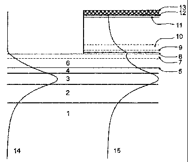
[0011] Figure 1 is a graphic representation of the layer structure and the
optical
field profile of the only vertical mode in the passive (left) and active
(right) portions of
the waveguide device;
[0012] Figure 2 is schematic layer structure and layout of the integrated WPD
with
end N-contacts;
[0013] Figure 3 is a schematic layer structure and layout of the integrated
EAA
with side N-contacts;
[0014] Figure 4 is a schematic layer structure and layout of the integrated
SOA
with lateral N-contacts;
SUBSTITUTE SHEET (RULE 26)
CA 02478071 2004-09-09
WO 02/077682 PCT/CA02/00194
[0015] Figure 5 is a graphic representation of the spatial distribution of the
TEo-
mode optical field at a wavelength of 1.55 pm in the passive and active
waveguide
portions of the embodiment with layer structure given in Table I;
[0016] Figure 6 is a graphic representation of the spatial distribution of TEo-
mode
optical field at a wavelength 1.55 pm in the passive and active waveguide
portions of
the embodiment with layer structure given in Tables IIA (solid line) and IIB
(dashed
line); and
[0017] Figure 7 is a simplified circuit diagram of an integrated EAA connected
to a
constant voltage supply through a resistive load.
Detailed Description of the Invention
[0018] Referring to. Fig. 1, an embodiment of the invention in the form of a
layered
structure of the passive waveguide portion is shown on the left half of Fig. 1
and a
corresponding layered structure of the active waveguide portion of a same
device is
shown on the right half of Fig. 1. The passive waveguide portion is designed
to be a
low-loss and low-birefringence waveguide. It comprises a number of layers
grown on
and lattice matched to the undoped substrate 1: a buffer layer 2, a waveguide
core layer
3, a lower cladding layer 4, an etch stop layer 5, and an upper cladding layer
with two
portions, 6 and 7, of which the top portion 7 is a heavily N-doped layer while
the layers
2-6 all are undoped. The structure of the active waveguide portion (shown on
the right
half of Fig. 1) includes additional layers on top of the passive waveguide
portion: an
undoped active layer 8, spacer layer 9, P-contact layers 10 and 11, a cap
layer 12 and a
metalization layer 13. The layers above the active layer 8 are produced such
that the
level of P-doping rises from a negligible value in the spacer 9 to a very high
(~1x10~~
cm 3) level in the cap. In this embodiment, the material of choice is InP and
related
compound semiconductors, so that layers 2, 4, 6, and 7 are InP layers, while
the
waveguide core 3 and etch stop 5 are quaternary GaInAsP layers, while the cap
layer 12
is a ternary GaInAs layer, all grown on and lattice matched to the InP
substrate. The
active layer 8 is the narrowest bandgap layer, and the material composition,
strain and
thickness of this layer are chosen on the basis of the device application, so
that the
SUBSTITUTE SHEET (RULE 26)
CA 02478071 2004-09-09
WO 02/077682 PCT/CA02/00194
bandgap Eb , defined as an energy separation between the lowest (sub)band in
the
conduction band and highest (sub)band in the valence band, is adjusted to the
operating
photon energy ~~ in some predetermined way. It may be a bulk ternary GaInAs
(photodetecting) or a quaternary GaInAsP (attenuating or amplifying) layer or,
alternatively, a photodetecting, attenuating or amplifying quantum well (QW)
layer
comprising one or more narrower bandgap wells separated by wider bandgap
barriers.
In this last case, either InGaAs/InP or InGaAsP/InP or InGaAs/InGaAsP or
InGaAsP/InGaAsP or InGaAs/InAIAs pairs of materials, lattice matched or
intentionally strained, are available as materials for well(s)/barriers. In
any case, the
entire layer structure is grown in a single step and then layers 8-12, absent
in the
passive waveguide portion, are etched out everywhere except in the active
waveguide
portion.
[0019] The properly designed layer structure ensures single vertical mode
propagation within a waveguide portion absent an active device (left half of
the Fig. 1)
and within a waveguide portion having an active device (right half of the Fig.
1), so that
the modes in the active and passive waveguide portions are substantially
matched in
terms of their propagation constants and field overlaps. Still, the profiles
of the modes,
indicated by 14 and 15 in Fig. l, differ due to their mode tails above the
passive
waveguide structure. While in the passive waveguide portion the optical field
14 above
the upper cladding drops sharply, in the active waveguide portion the optical
field 15
has a formation in the form of a peak or shoulder in the active layer 8, since
this layer
has a narrower bandgap and hence a higher refractive index than N- and P-
contact InP
layers below and above it. The mode field then drops smoothly towards the top
metallization layer(s). Due to an overlap between the waveguide mode 15 and
active
layer 8, even though a relatively small one, light propagating through the
active
waveguide portion experiences either interband transition induced
photodetection in the
spectral range above the bandgap ( ~~ > Eb ), or an electric field assisted
interband
absorption somewhat below the bandgap ( t~~ < EK ), or carrier injection
produced
interband amplification in the spectral range about the bandgap ( ~c~ ~ E~ ),
depending
on the device application . The response of the device is controlled through
an electric
bias applied between N- and P-contact layers on both sides of the active layer
8, which
SUBSTITUTE SHEET (RULE 26)
CA 02478071 2004-09-09
WO 02/077682 PCT/CA02/00194
is reverse bias in a case of photodetection or electro-absorptive attenuation
and forward
bias in a case of amplification. It also depends on the confinement factor of
the
waveguide mode 15 with the active layer 8, which is limited by the requirement
for
having no more than one vertical mode in either TE (electric field of the mode
in the
plane of epitaxial growth) or TM (magnetic field of the mode in the plane of
epitaxial
growth) polarizations, for one thing, and the desire to minimize coupling loss
and
reflection at junction between the active and passive waveguide portions, for
another.
In a properly designed layer structure, the confinement factor of the only
vertical mode
with the active layer is about 1-2% which apparently limits the performance of
the
device. However, such a limitation is not critical for applications in
relatively low
speed WDM components. This is because a small overlap between the waveguide
mode and the active layer atop the passive waveguide portion is easily
compensated by
increasing the length of the active waveguide portion, once device speed,
limited by the
capacitance, is not of concern. Practically, lengths a few mm for the active
portion of
the waveguide device would be sufficient for most applications.
[0020] At first glance, the layer structure shown in Fig. 1 is similar to that
of a
standard evanescent-field coupled device, e.g. integrated WPDs described in
many
earlier publications and exhaustively reviewed by R.G. Deri in "Monolithic
Integration
of Optical Waveguide Circuitry with III-V Photodetectors for Advanced
Lightwave
Receivers", IEEE J. Lightwave Technol., Vol. 11, P. 1296, 1993. However, there
is a
fundamental difference between the two. The standard scheme of evanescent-
field
coupling implies that there is at least one more vertical mode in the active
waveguide
portion, with the field maximum within the active layer, and relies on a
transfer of the
single mode of the passive waveguide portion into this (those) higher models).
On the
contrary, the integration method disclosed herein is based on the assumption
that there
is only one vertical mode (in each polarization) in the active waveguide
portion, and
that this mode substantially matches that of the passive waveguide portion. As
a result,
coupling between the active and passive portions of the two-section waveguide
device
is stable ,(high reproducibility from growth to growth) and very efficient.
The stability
of the coupling is due in part to a lack of intermode interference, since
either section
supports only one vertical mode. This type of performance is difficult to
achieve with a
standard evanescent-field vertical integration scheme according to the prior
art, e.g.
SUBSTITUTE SHEET (RULE 26)
CA 02478071 2004-09-09
WO 02/077682 PCT/CA02/00194
M.R. Amersfoort et al, "Low-Loss Phased Array Based 4-channel Wavelength
Demultiplexer Integrated with Photodetectors", IEEE Photon. Technol. Lett,
Vol. 6, P.
162, 1994; R. J. Deri, "Monolithic Integration of Optical Waveguide Circuitry
with III-
V Photodetectors for Advanced Lightwave Receivers", IEEE J. Lightwave
Technol.,
Vol. 11, P. 1296, 1993; and K. Steenbergen, "High-Capacity Integrated Optical
Receivers", Ph. D. Thesis Delft University of Technology, The Netherlands,
1997.
[0021] The operation principles of specific devices using the integration
method
disclosed above, which is labeled as single-mode vertical integration, are now
discussed with reference to Figs. 2-4. The details of the layer structure and
numerical
examples are given by assuming InP-based devices designed for operating in C-
band of
I.SSpm communication window at room temperature. It is apparent to those of
skill in
the art that though those details and examples provide a variety of
embodiments, other
layer structures and materials are also employable within the spirit and scope
of the
invention.
[0022] Figs. 2-4 show the schematic layer structure and layout of possible InP-
based waveguide devices using the single-mode vertical integration method. It
is
assumed that active devices may be integrated within passive waveguides of
single-
wavelength channels of planar WDM components, such as optical
(de)multiplexers,
and thus form an array of devices operating in different wavelengths. The
devices
shown in Figs. 2-4 are similar in their layer structures 1-11 (to extend that
the active
layer 8 is specific to the embodiment, see below) and layout of P-contacts 12,
but
different in the layout of their N-contacts) 13. This difference reflects two
fundamental
restrictions on device performance, associated with having the N-contact layer
7 of
limited thickness and separated by limited distance from the waveguide core 3.
First,
the optical field on the upper boundary of the N-contact layer, even though it
is
relatively small, is not negligible. Otherwise it would not be coupled into
the active
layer 8 just above N-contact layer 7. It follows that the metal of the N-
contacts 13
deposited on the N-contact layer 7 will introduce a certain amount of loss,
should they
be placed at the ends of the active portion of the waveguide device as shown
in Fig. 2.
Furthermore, this loss will be a polarization dependent loss (PDL) that
results from the
fact that the TM mode has higher optical field in the end N-contact than TE-
mode. The
SUBSTITUTE SHEET (RULE 26)
CA 02478071 2004-09-09
WO 02/077682 PCT/CA02/00194
problem is, however, solved by replacing the end N-contacts shown in Fig. 2
with the
side N-contacts shown in Fig. 3. Second, an N-contact layer 7, of limited
thickness and
doping level, has substantial sheet resistance. In the device with either end
or side N-
contacts, shown in Figs. 2 and 3, respectively, this results in a significant
series
resistance. Current flowing through this resistance may consume most of the
applied
electric bias and, additionally, lead to a release of substantial Joule power
that would
heat up the entire device and degrade its performance. Series resistance is
reduced by
about three orders of magnitude when the lateral N-contacts, shown in Fig. 4,
are used
rather than end or side N-contacts.
Example: Integrated Waveguide Photodetector
[0023] An exemplary embodiment of the invention in application to an
integrated
WPD, with the layer structure specified in Table I, and the device layout
illustrated in
Fig. 2, was designed and modeled. The epitaxial layers may be divided into two
groups:
waveguide layers (2-7) and photodetector layers (8-11). The device also has
two metal
contacts 12 and 13 of Fig. 2 (not present in Table I). The passive waveguide
is designed
to be a single-mode, low birefringence guide. This is a straightforward design
used in
planar waveguide demultiplexers, e.g. those described by E. S. Koteles in
"Integrated
Planar Waveguide Demultiplexers for High-Density WDM Applications", Wavelength
Division Multiplexing. A Critical Review, CR71, R. T. Chen & L. S. Lome, ed.,
SPIE,
Bellingham, P. 3, 1999. Most of the optical mode in eitherTE or TM
polarization is
confined within the waveguide core 3, which is a relatively thick (0.6 p.m)
and low As
composition (15.6%) quaternary layer. However, the overall thickness of the
InP
cladding layers above the core is just 1.05 p,m, which allows the tail of an
optical mode
to reach the upper boundary of the waveguide. The N-doped upper part (0.25 p.m
in this
particular structure) 7 of the InP cladding also serves as the N-contact layer
of the
planar PIN photodiode. Where this layer is disposed on top of the passive
waveguide
portion, as is the case in an active waveguide portion of the integrated WPD,
the
propagating light penetrates the photodetector layers. Both waveguide portions
operate
in a single vertical mode, which does not change substantially when light
propagates
from the passive to active portion of the waveguide as shown in Fig. 5. The
effective
index difference between the TEo-mode in the active and passive waveguide
portions of
to
SUBSTITUTE SHEET (RULE 26)
CA 02478071 2004-09-09
WO 02/077682 PCT/CA02/00194
integrated WPD with the layer structure shown in Table 1 is as little as
0.002, i.e.
about 0.06%, while the mode field overlap between these two waveguide portions
is
about 0.952, corresponding to only 0.43 dB coupling loss in a slab waveguide
geometry. In layman's terms, the active and passive waveguide portions of the
integrated WPD are approximately mode matched. Still, there is a difference in
the
shapes of the mode in the active and passive waveguide portions that allows
the mode
to overlap the absorbing active layer 8. Although the confinement factor
corresponding
to the absorbing layer, hA , is low - about 1.21% for TE polarization and
0.68% for TM
polarization - the mode coefficient of absorption, a , which is substantially
due to
interband transitions within the active layer, is fairly high - about 4.7x10²
dB/cm and
2.6x10² dB/cm in TE- and TM-polarizations, respectively. Thus a reasonably
long
active waveguide portion will absorb and detect all the light, coupled to this
active
waveguide portion, in any polarization state. For the given exemplary layer
structure of
Table I, a WPD of just 1 mm length detects practically all the incoming light
in either
TE or TM polarization, with only 0.22% difference between the photocurrents
associated with these two polarizations.
TABLE I: Possible Layer Structure of InP-based Monolithically
Integrated WPD for Operating in 1.SS~tm
Communication Window at Room Temperature
No Layer Material's Doping Thickness
1 SubstrateInP U/D 350+ pm
2 Buffer InP U/D 1.0 pm
3 Core InGaAsP[~,g U/D 0.6 ~tm
l.Opm]
4 CladdingInP U/D 0.3 p,m
Etch InGaAsP[~,g U/D 0.005
stop 1.3p,m] p.m
6 CladdingInP U/D 0.5 p.m
7 N-contactInP:S Sx10~8 0.25 pm
cm 3
~~ All layers are lattice matched to InP substrate. Shown in parenthesis are
the wavelengths corresponding
to the bandgap in quaternary layers.
SUBSTITUTE SHEET (RULE 26)
CA 02478071 2004-09-09
WO 02/077682 PCT/CA02/00194
No Layer Materiah~ Doping Thickness
8 AbsorbingInGaAs U/D 0.065
~.m
9 Spacer InP U/D 0.065
~m
P-contactInP: Zn 1 x 10 0. 3 ~.m
~ ~
cm 3
11 P-contactInP:Zn 1x10'$ 0.7 p,m
cm 3
12 Cap InGaAs:Zn 1x10¹⁹ 0.1 ~m
cm 3
[0024] A WPD, as an end-point device in WDM components like optical power
(channel) monitors, has to provide an estimate for optical power P~ in a
single
wavelength channel with photon energy ~~ by measuring the photocurrent J~, in
this
particular channel, which is physically separated from other channels by a
demultiplexer. Two important characteristics of this device are the
responsivity Ot~, and
dynamic range ~P~,",;n,P~,",~X~ . BY assuming that the active waveguide
portion is long
enough to completely absorb all the light coupled into this portion, the
former is
defined as
'~~ = p = ~7c~7r ~~ (1)
W
with ~jc as the coupling efficiency between the active and passive waveguide
portions,
~P as the quantum yield in the active waveguide portion, and a as the charge
of an
electron. In the ideal device with both ~c and riP equal to unity, the
responsivity at
1.55 ~m wavelength would be 1.25 A/W. The actual responsivity of the WPD is
somewhat lower, due to coupling loss, recombination loss, and propagation loss
independent from interband absorption. Coupling loss in the slab waveguide
with a
layer structure given in Table I is roughly 0.43 dB, which is somewhat more
than that
in the ridge waveguide shown in Fig 2 with an otherwise equivalent layer
structure.
Recombination of photogenerated carriers in a PIN double heterostructure with
that
thin narrower bandgap absorbing layer and with a quality of heterointerfaces
typical for
12
SUBSTITUTE SHEET (RULE 26)
CA 02478071 2004-09-09
WO 02/077682 PCT/CA02/00194
modern growth techniques is substantially negligible. Then, the quantum yield
photogeneration efficiency - is determined as
are ~2)
~lr=ao+a,B'
where a,B and coo are the contributions of the interband transitions in the
absorbing
layer 7 and all the other mechanisms of propagation loss, respectively, to the
mode
coefficient of absorption a = ao + a,B . Typically, ao does not exceed a
couple of
dB/cm, while a,Q is well in the hundreds of dB/cm, i.e. even in a WPD with a
very thin
absorbing layer the quantum yield is close to unity. That brings us to an
estimate of
responsivity as ~Ji~, >_ 1.1 AlW , which indeed is a very high value for this
parameter.
[0025] The dynamic range of the device is determined as an input power window,
within which a registration of the photocurrent occurs with a certain level
of~
confidence. Minimum input power in each wavelength channel, P~,m;~ , is
limited by the
noise and dark currents of a photodiode. Assuming room temperature operation
and
taking into account that the electric passband of the device is restricted by
its RC-time
constant and thus amounts to 100 MHz for a 1 mm long device, it is easily
found that
the noise current is dominated by the shot noise. It is estimated as ~16 pA
for a device
with the layer structure given in Table I, that would result in P~,m~~ W80
dBm, should
the noise be a limiting factor. Most probably, however, it is the. dark
current that limits
the detected optical power on the low power side. Still, the dark current 300
pA at
reverse bias of ~ -S V in lrrun long device with the layer structure given in
Table I is
not seen to be unreasonable, which suggests that P~,m~~ 0 -65 dBm, at the very
least. As
to the maximum input power, P~ max , this is limited primarily by nonlinear
saturation
effects in the process of photodetection. This process relies on collecting
the
photocarriers, generated in the absorbing layer 8, by the N- and P-contact
layers below
and above that layer, respectively. An efficient collection of photocarriers
requires high
electric field in the absorbing layer and adjusted space-charge regions of the
contact
layers that is normally reached by reverse electrical biasing of the PIN
structure.
However, it is expected that at high optical powers, either the electric field
in the
13
SUBSTITUTE SHEET (RULE 26)
CA 02478071 2004-09-09
WO 02/077682 PCT/CA02/00194
absorbing layer will be screened by photocarriers or the local reverse bias
will be
reduced by the voltage drop in the contact layers, caused by the photocurrent.
In the
particular case of the integrated device disclosed herein, the second
mechanism is more
important, since the very principle of the single-mode vertical integration
assumes that
the N-contact layer 7 is quite resistive. The voltage drop dV across the N-
contact layer
of length QN , assuming that the only metal contact to this layer is
positioned at the
output end of the active portion of the waveguide device, is estimated as
dV D ~NPN ~~ p~
WN
where 2N , wN and pN = Il(euNNdN) are the length, width and sheet resistance
of the
N-contact layer 7, respectively, with ,uN as the electron's mobility, N as the
concentration of electrons and dN as the thickness of the N-contact layer. In
a device
with the layer structure of Table I, the sheet resistance is estimated as pN ~
40 S2 . By
taking ~N (J 1 mm and wN 0 4 Eun as reasonable values for the length and width
of the
N-contact layer, respectively, Eq. (3) predicts a voltage drop of about 10 V
for each
mW of the input optical power. Because of this voltage drop, the actual
reverse bias of
a PIN structure is lower than that applied between the contacts, the
difference between
the two growing with increasing distance from the N-contact. Assuming a
typical
operating voltage of -5 V, which is the voltage 14 (15) between the P- and N-
contacts,
12 and 13, respectively, in Fig. 2, and admitting that the reverse bias in any
point across
the WPD should not be above -2 V, one finds that high electric resistance of
the N-
contact layer 7 limits the input optical power to P~,,",aX ~ -5 dBm.
Optionally, if the
dynamic range of WPD has to be extended towards higher powers, another N-
contact is
positioned at the input end of the active portion of the device or,
alternatively, two or
more side N-contacts, such as those shown in Fig. 3, are used rather than the
end N-
contacts.
14
SUBSTITUTE SHEET (RULE 26)
CA 02478071 2004-09-09
WO 02/077682 PCT/CA02/00194
Example: Integrated Electro-Absorptive Attenuator
[0026] Also, an exemplary embodiment of the invention in application to an
integrated EAA, with the layer structure specified in Table IIA and the device
layout
illustrated in Fig. 3, was designed and modeled. The distribution of the
vertical mode
field in the passive and active waveguide portions is shown in Fig. 6. The
layer
structure of the integrated EAA is similar to that of the integrated WPD, an
embodiment disclosed above. The only difference appears in the material of the
active
layer 8 and also in the thickness of the spacer layer 9 ixmnediately above the
active
layer. The interband absorption in the active layer, which is still the
narrowest bandgap
layer but now has the bandgap energy slightly above the operation photon
energy,
occurs only in a relatively high electric field. Some increase in the spacer
thickness
improves the overlap between the optical mode field and electric field of PIN
structure.
The layout of the device also is similar to that of the WPD. However, even
though end
N-contacts such as those shown in Fig. 2 also are employable in this
embodiment,
higher operating power and lower tolerance to insertion loss in applications
for which
EAA is intended, such as dynamic channel equalization, make the design using
the side
N-contacts shown in Fig. 3 preferable. One or more side N-contacts 13
schematically
shown in this figure are optionally positioned anywhere along the active
portion of the
waveguide device. This configuration eliminates PDL associated with the end N-
contacts and, in a case of multiple side N-contacts, substantially reduces the
voltage
drop across the N-contact layer. At the same time, it introduces some extra
loss, similar
to that at a waveguide crossing. It is felt, however, that a proper design of
the side N-
contacts 13 will keep this loss at a level well below 0.1 dB per crossing, as
is the case
with conventional waveguide crossing, e.g. reported by H. G. Bulckems et al,
in
"Minimization of the loss of integrated waveguides in InP-based photonics
integrated
circuits", IEEE Photonics Technol. Lett., Vol. 11, P. 1420, 1999.
SUBSTITUTE SHEET (RULE 26)
CA 02478071 2004-09-09
WO 02/077682 PCT/CA02/00194
TABLE IIA Possible layer structure of InP-based monolithically
integrated EAA with a bulk active layer for operating in
1.55~,m communication window at room temperature.
No Layer Material's Doping Thickness
1 Substrate InP U/D 350+ ~m
2 Buffer InP U/D 1.0 p,m
3 Core InGaAsP[~,~ U/D 0.6 ~,m
1.0~m]
4 Cladding InP U/D 0.3 ~m
Etch stop InGaAsP[~,g U/D 0.005
l.3pm] ~.m
6 Cladding InP U/D 0.5 ~m
7 N-contact InP: S 5x 10 0.25 ~,m
~ g cm
3
8 Electro-AbsorbingInGaAsP[~,g=1.43~.m]U/D 0.08 ~,m
9 Spacer InP U/D 0.12 ~.m
P-contact InP:Zn 1x10" 0.3 ~m
cW 3
11 P-contact InP:Zn 1x10$ 1.5 ~m
cm 3
12 Cap InGaAs:Zn 1x10'9 0.1 ~,m
cm 3
[0027 The operation principles of this embodiment in form of an integrated EAA
are based on controlling the interband absorption in the active layer 8, in
the spectral
range of photon energies somewhat below the bandgap in this layer, ~C~ < E~ ,
by
changing the vertical quasi-static electric field F therein. In the embodiment
disclosed
in Table IIA, the electro-absorbing layer 8 is a bulk direct-gap semiconductor
material
wherein the mechanism of absorption below the bandgap is associated with
electric
field assisted interband tunneling, known as the Franz-Keldysh effect (FKE)
and first
reported by W. Franz in Z. Naturforsch. T. A 13, P. 484, 1958 and L.V. Keldysh
in Zh.
~~ All layers are lattice matched to InP substrate. Shown in parenthesis are
the wavelengths corresponding
to the bandgap in quaternary layers.
16
SUBSTITUTE SHEET (RULE 26)
CA 02478071 2004-09-09
WO 02/077682 PCT/CA02/00194
Exp. Teor. Fiz., T. 34, S. 1138, 1958 (Sov. Phys. -.IETP, Vol. 7, P. 788,
1958). The
quasi-static electric field in the active layer 8 is tuned by alternating the
reverse electric
bias 14 (15) of the PIN structure, according to the sketch of a waveguide
device shown
in Fig. 3. The device design is such that at zero bias field-assisted
interband transitions
in the active layer 8 are not very probable and, therefore, the active
waveguide portion
has a relatively low propagation loss. However, the probability of field-
assisted
interband tunneling and hence the absorption loss grows with an increase of
reverse
bias. As a result, the transmission of this active waveguide portion is
controlled by the
reverse bias of the P1N structure. Thus, the integrated EAA operates as a
voltage-
controlled variable optical attenuator, in contrast to most previous art using
current-
controlled devices, such as, those based on a phase modulation in branches of
a Mach-
Zehnder interferometer due to thermo-optical effect, as reported by C.R. Doerr
et al, in
"Dynamic Wavelength Equalizer in Silica Using the Single-Filtered-Arm
Interferometer", IEEE Photon. Technol. Lett., Vol. 11, P. 581, 1999; or the
free-carrier
plasma effect, as reported by LE. Day et al, "Solid-State Absorption
Attenuator in
Silicon-on-Isolator with MHZ Bandwidth", Paper Presented at NFOEC'01, 2001. As
inthe case of any variable optical attenuator, which is an in-line optical
component with
light propagating through, the important characteristics of the device
described by this
embodiment are the insertion loss and dynamic range.
[0028] The insertion loss is determined by the loss in the N-contacts, which
in the
case of side contacts shown in Fig. 3 is the crossing loss, coupling loss at
junctions
between the active and passive waveguide portions, and propagation loss,
mainly in the
active waveguide portion. As mentioned above, the crossing loss with proper
design
and fabrication is easily reduced well below 0.1 dB per crossing. Coupling
loss is
estimated by the overlap integral between the mode fields in the active and
passive
waveguide portions of the integrated EAA and amounts to ~0.3 dB per single
pass for
the embodiment with the layer structures given in Table IIA. Propagation loss
in the
active portion of the waveguide device is primarily due to residual
electroabsorption in
the unbiased PIN structure, although intervalence band absorption in the P-
contact
layers provides some contribution as well. The resulting propagation loss of
the guided
mode is estimated as
17
SUBSTITUTE SHEET (RULE 26)
CA 02478071 2004-09-09
WO 02/077682 PCT/CA02/00194
a~(V) = a° + I-'~(V)A~(V) , (4)
where the first and second teens on the right hand side account for the loss
disconnected from the interband absorption and that due to interband
absorption,
respectively, with Tw (V ) and A~, (V ) as the mode confinement factor and
material
absorption corresponding to the active layer 8, both functions of the electric
bias V .
Then, the contribution of the propagation loss to the insertion loss is
determined as the
propagation loss at zero bias, i.e. a~(0) = a° + T~(0)A~(0) . For the
embodiment with
the layer structure given in Table IIA, a° is expected to be about 1
dB/cm, assuming
state of the art growth and fabrication technologies that reduce the
scattering loss in the
transparent ridge waveguides to just a fraction of dB/cm, e.g. as reported by
R. J. Deri
et al, in "Low-loss III-V Semiconductor Optical Waveguides", IEEE J. Quantum
Electron., Vol. 26, P. 640, 1991. For the same embodiment, the confinement
factor of
the single waveguide mode with the active layer 8 is roughly 1% (~1.2% for TE-
polarization and ~0.8% for TM-polarization). These values do not depend much
on the
bias since the device is designed for electroabsorption rather than for
electrorefraction.
The material absorption, Aw, has a sharp and highly nonlinear dependence on
the
electric field, F , in the active layer and also is very sensitive to the
deficit of photon
energy therein, Es - W v > 0 , both due to the tunneling nature of the
electroabsorption
below the bandgap. At the same time, the material absorption in the bulk
active layer
does not really depend on the polarization of light. For the embodiment with
the layer
structure given in Table IIA, at zero bias F <- 4x10⁴ V/cm which ensures that
h~,(0)A~,(0) <_ I dB/cm across the entire C-band in either polarization.
Overall, the
insertion loss of the EAA with the layer structure of Table IIA and a 2 mm
long active
portion, which combines the contact, coupling and propagation loss, is roughly
1 dB at
the blue edge of C-band and somewhat less (~0.8 dB) at the red edge of C-band.
[0029] The dynamic range of the integrated EAA is determined by its variable
attenuation range and the input power range that enables this attenuation
range. The
attenuation range is defined as a maximum to minimum transmission ratio, where
maximum and minimum transmissions are those at zero and the highest possible
18
SUBSTITUTE SHEET (RULE 26)
CA 02478071 2004-09-09
WO 02/077682 PCT/CA02/00194
reverse biases, respectively. The upper limit of the reverse bias apparently
is restricted
by electric breakdown of the PIN structure, but it also depends on the design
of the
voltage controller. By any account, however, a reverse bias of up to ~12 V
does not
seem to be unreasonable considering the embodiment given in Table IIA. At such
a
bias, the electric field in the active layer reaches F ~ 3.6x10⁵ V/cm which
brings the
material electroabsorption therein above 1.8x103 cm' even at the red edge of C-
band,
resulting in at least 15 dB attenuation range over the entire C-band. In fact,
the variable
attenuation range is well above 15 dB for most wavelengths within this band.
The
lower limit of the input power range, within which 15 dB range of attenuation
is
achievable, is really limited only by the noise floor of the optical signal.
On the higher
power side, the limitation is due to the same saturation effects as those
discussed above
referring to the embodiment in the form of the WPD. The major one is
associated with
the voltage drop across the highly resistive N-contact layer 7, caused by the
photocurrent generated as a result of interband electroabsorption in the
active layer 8.
This voltage drop reduces the actual bias of the PIN structure V(x) , which
becomes a
function of the coordinate in the direction of propagation, x . Since the
coefficient of
the interband absorption and hence the propagation loss heavily depend on the
local
bias of the PIN structure, both are suppressed by photogeneration which is
seen as
saturation of the electro-absorptive attenuation at high optical powers.
Propagation in
such a nonlinearly absorbing active waveguide portion is optionally described
through
the coordinate dependence of the optical power, P~,(x), and bias voltage,
Y(x), which
have to satisfy the system of nonlinear equations:
=-[aw +cr~ (V)'P~,
dZV __ _ ePN ~e '
dx2 ~t~wN a~' (Y)Pw
where a~ (Y) =T~,(Y)A~(V) is the contribution from the interband
electroabsorption
in the active layer to the propagation loss of the mode. The boundary
conditions to
these equations are formulated in terms of the optical power at the start of
the active
waveguide portion and the electric bias of the PIN structure on each N-
contact.
Numerical simulations based on these equations predict that for an embodiment
with
19
SUBSTITUTE SHEET (RULE 26)
CA 02478071 2004-09-09
WO 02/077682 PCT/CA02/00194
the layer structure given in Table IIA, 3-4 side N-contacts of the kind shown
in Fig. 3
will keep the voltage drop between the contacts below 1 V, provided the input
optical
power is equal to or below S dBm. Thus, the EAA described herein is expected
to
provide at least 1 S dB variable attenuation for an optical signal with a
power at the
device input port up to 5 dBm in a spectral range over the entire C-band at a
voltage
equal to or below 12 V. Given that this device has a transient time limited by
its RC-
constant, similar to the previously described embodiment in the form of a WPD,
the
electrical bandwidth of the EAA with a 2-mm long active portion is estimated
to be
roughly 25 MHz.
[0030] Yet another exemplary embodiment of the invention in the form of an
integrated EAA has the layer structure specified in Table IIB and a device
layout
illustrated in Fig. 3. The distribution of the vertical mode field in the
passive (solid line)
and active (dashed line) waveguide portions is shown in Fig. 6. This device is
similar to
that disclosed above referring to Table IIA but has QWs rather than bulk
semiconductor
material for the electro-absorbing active layer 8. Specifically, this is a
stack of 6 44-mn
quaternary Gao,o~,Ino,9z9Aso,,~~Po.sz9 layers as barriers and 5 7-nm ternary
Gao,6lno,4As
layers as wells. These ternary wells are strained in a tensile manner at about
0.9%,
while the quaternary barriers are compressively strained, to a much lesser
degree of
0.05%. The resulting quantum subband structure is such that the upper hole
subband is
the light hole subband corresponding to a bandgap wavelength of about 1430 nm
and
the bandgap involving the heavy hole subband is some 20-25 nm shorter, in
terms of
bandgap wavelengths. It is well known that inverting the relative positions of
the light
and heavy hole subbands, achieved byintroducing a certain amount of
controllable
tensile strain into the wells, are optionally used for enhancing the intensity
of interband
transitions in the TM polarization (magnetic field of the optical signal in
the plane of
the wells) versus the TE polarization (electric field of the optical signal in
the plane of
the wells), as reported by J.E. Zuker et al, in "Optical Transitions in
Strained
InGaAs/InGaAs Quantum Wells", IEEE Photonics Technol. Lett., Vol. 4, P. 432,
1992;
or Cheung et al, in US Patent No 5,117,469 (5/1992). Also, a QW active layer
optically
behaves as a uniaxially anisotropic material, which has slightly different
refractive
indexes in the TE and TM polarizations. When the wells are strained in a
tensile
manner as described above, the material birefringence of the QW active layer
is such
SUBSTITUTE SHEET (RULE 26)
CA 02478071 2004-09-09
WO 02/077682 PCT/CA02/00194
that light in the TM polarization sees higher refractive index than light in
the TE
polarization, as reported by Zucker in US Patent No 5, 090, 790 (2/1992); or
by J.E.
Zuker et al, in "Strained Quantum Wells for Polarization-Independent
Electrooptic
Waveguide Switches", J. Lightwave Technol., Vol. 10, P. 1926, 1992. As a
result, the
confinement factor of the TM-mode with the active layer increases and
approaches that
of the TE-mode, which in a waveguide made up from optically isotropic
materials, is
higher, as described in the textbook "Theory of Dielectric Optical
Waveguides", 2°a
ed., Academic Press, 1991 by Marcuse. For an embodiment with the layer
structure
given in Table IIB, the confinement factor with the active layer is 1.74% for
the TE-
mode and 1.68% for the TM-mode.
TABLE IIB Possible Layer Structure of InP-based Monolithically
Integrated EAA With a Tensile-Strain Quantum Well Active
Layer for Operating in 1.SS~m Communication Window at
Room Temperature
No Layer Material's Doping Thickness
1 Substrate InP U/D 350+ ~.m
2 Buffer InP U/D 1.0 ~.m
3 Core lnGaAsP[~,g l.Opm] U/D 0.6 yn
4 Cladding InP U/D 0.3 p.m
Etch stop InGaAsP[~,g 1.3p.m] U/D 0.005
~m
6 Cladding InP U/D 0.5 p,m
7 N-contact InP:S Sx10t8 0.25 pm
cm 3
6 x 44nm CS InGaAsP(barrier)
8 Electro-Absorbing+ U/D 0.3 ~m
5 x 7.2nm TS InGaAs(well),
~ =1.43 m LH1-C1 band
a
9 Spacer InP U/D 0.02 p,m
'~ All the layers except those of electro-absorbing QW stack, are lattice
matched to lnP substrate. Shown
in parenthesis are the wavelengths corresponding to the bandgap in quaternary
layers. InGaAs QWs in
electro-absorbing layer are tensile strained, InGaAsP barriers are,
optionally, slightly compressive
strained. Bandgap of ~1.43ttm in this layer is determined by the upper light
hole subband, which is above
the upper heavy hole subband due to a tensile strain.
21
SUBSTITUTE SHEET (RULE 26)
CA 02478071 2004-09-09
WO 02/077682 PCT/CA02/00194
No Layer Material's Doping Thickness
P-contact InP:Zn 1x10'7 0.3 pm
cm 3
11 P-contact InP:Zn 1x101$ 1.5 ~m
cm 3
12 Cap InGaAs:Zn 1x10¹⁹ 0.1 ~.m
cm 3
[0031] The operating principle of this embodiment is similar to that of the
embodiment disclosed in Table IIA and discussed above. Still, there is a
difference in
the actual characteristics of the device that is due to a difference in the
mechanism of
electroabsorption between the bulk and QW active layers. A quasi-static
electric field
applied in the direction of growth shifts the electron's and hole's dimension
cjuantization levels towards each other, on one hand, and broadens these
levels due to
field-assistant tunneling, on another. This phenomenon, known as the quantum
confined Stark effect (QCSE) and first reported by D.A.B. Miller et al, in
"Band-Edge
Electroabsorption in Quantum-Well Structures: The Quantum-Confined Stark
Effect",
Phys. Rev. Lett., Vol. 53, P. 2173, 1984, is seen as an electric field induced
increase in
the iriterband absorption in a spectral range somewhat below the band gap. The
electroabsorption in the QW active layer is determined mostly by the red shift
of
effective the bandgap at lower electric fields and tunnel broadening of the
absorption
edge at higher electric fields. In the classic limit, i.e. wide QWs with a
small energy
separation among the dimension quantization levels, the QCSE is naturally
reduced to
the FKE, as was shown by D.A.B. Miller et al, in "Relation Between
Electroabsorption
in Bulk Semiconductors and in Quantum Wells: The Quantum-Confined Franz-
Keldysh Effect", Phys. Rev. B, Vol. 33, P. 6976, 1986. The details of the
electroabsorption in QWs have been well studied both theoretically and
experimentally,
e.g. in publications: D.A.B. Miller et al, "Electric Field Dependence of
Optical
Absorption Near the Band Gap of Quantum-Well Structures", Phys. Rev. B, Vol.
32, P:
1043, 1985; D.A.B. Miller et al, "Electric-Field Dependence of Linear Optical
Properties in Quantum Well Structures: Waveguide Electroabsorption and Sum
Rules",
IEEE J. Quantum Electron., Vol. QE-22, P. 1816, 1986; and S. Schmitt-Rink et
al,
"Linear and Nonlinear Optical Properties of semiconductor Quantum Wells",
Advances
in Physics, Vol. 38, P. 89, 1989. These references teach that the absorption
edge in QW
22
SUBSTITUTE SHEET (RULE 26)
CA 02478071 2004-09-09
WO 02/077682 PCT/CA02/00194
material is generally sharper than that in bulk semiconductors with
approximately the
same bandgap energy and that this difference is preserved over a range of
electric fields
up to several units of 105 V/cm. With regards to the EAA performance, this
means a
lower insertion loss and a higher dynamic variable attenuation range in a
device with a
QW active layer as compared to the device with a bulk active layer. For an
embodiment
with the layer structure given in Table IIB, at zero bias the electric field
in the active
layer is about F ~ (3-4)x104 V/cm which ensures h~(0)A~,(0) <_ 0.2 dB/cm
across the
entire C-band for either TE- or TM-polarization. The total insertion loss of
the
integrated EAA with 2-mm long active waveguide portion, which combines
contact,
coupling and propagation loss, does not exceed 0.6 dB in the C-band. As for
the
variable attenuation range, the reverse electrical bias of 12 V produces
roughly a
3.1x10⁵ V/cm strong electric field in the active layer of the embodiment
specified in
Table IIB, resulting in a material absorption therein of A~, >_ 1.3x103 cm ~
and a mode
attenuation of 20 dB or more over the entire C-band. The range of the input
power that
enables this dynamic range of variable attenuation is limited by the same
nonlinear
saturation effects, associated with a photocurrent-induced voltage drop on the
sheet
resistance of the N-contact layer 7, as was discussed above referring to the
embodiment
specified in Table IIA. Again, assuming 3-4 side N-contacts of a kind shown in
Fig. 3
and requiring that the voltage drop between the contacts does not exceed 1 V,
one finds
that the optical power at the input of the active waveguide portion is limited
to roughly
dBm.
[0032] Besides the variable attenuation, the embodiment of the invention in
the
fornl of an integrated EAA, irrespective of the structure of the device active
layer and
the mechanism of electroabsorption therein, is also employable for detecting
the optical
signal propagating within the device. This is a natural feature of the EAA,
which
attenuates the light due to electric field assisted interband absorption in
the device
active layer. Electrons and holes generated in this layer are separated by the
high
electric field resulting in a photocurrent estimated, accordingly to Eqs. (5),
as
e~.
~m=~ml'm.rn= a ~~~a~BLv(x)lp~(x)= WN dvl >0. (6)
~t CO o PN dx X=o
23
SUBSTITUTE SHEET (RULE 26)
CA 02478071 2004-09-09
WO 02/077682 PCT/CA02/00194
[0033] Here, P~,.;n is the input optical power at photon energy ~xr.~ and it
is assumed
that x = 0 corresponds to the input of the active waveguide portion. At every
given
photon energy t~to, the photocurrent is a function of the input optical power
P~,,;n and
bias voltage applied between the P- and N-contacts of the PIN structure, VB .
The
functional dependence .Iw(P~,,;~,VB) is determined through either direct
calibration
measurements or simulations or both. The same is applicable to the relative
electro-
absorptive attenuation, T~(P~,;n,Ve), determined, accordingly to Eqs. (S), as
e~
T~, = I'~,o", l P~,,;" = exp ~- ( dx ~ c~~ ~V (x)~~ , (7)
0
where P~,o"~ is the output optical signal. At a given photon energy ~r.~ it is
also a
function of the input optical power P~.;" and bias voltage VB, which are
optionally
tabulated by using calibration measurements or/and simulations. Once
J~,(P«,;",VQ) and
T~(P~.;n, VB ) are known - they are provided, for example, in look-up tables -
the EAA
is employable as an optical power controller, which combines both optical
power
monitoring and variable optical attenuating functions. It is worth noting that
despite
various combinations of attenuating and photodetecting functionalities that
have been
suggested for device applications in the prior art, none of them have been
focused on
optical power controlling. So, the device proposed by R.B. Westland et al, in
"Dual
Function Electro-Absorption Waveguide Modulator/Detector for Optoelectronic
Transceiver Applications", IEEE Photon. Technol. Lett., Vol. 8, P. 1540, 1996,
operates either as an electroabsorption modulator or a photodetector, but by
no means
was the photocurrent generated by electroabsorption therein used for driving
the
modulator. The integrated device proposed by N. Yokouchi et al, in
"GaInAsP/InP
Attenuator Integrated Waveguide Photodetector (AIPD) Based on the Franz-
Keldysh
Effect", 10'x' Intern. Conf. On Indium Phoshide and Related Materials, 11-15
May
1998, Tsukuba, Japan, and also disclosed by N. Yokouchi et al, in US Patent No
5,973,339 (10/1999), does have a feedback electric circuit that enables
driving the
attenuator by analyzing the photocurrent. However, this device has two P-
electrodes
and two separate active waveguide portions: one for attenuating and one for
24
SUBSTITUTE SHEET (RULE 26)
CA 02478071 2004-09-09
WO 02/077682 PCT/CA02/00194
photodetecting, these portions have different layer structures and are butt-
coupled by
using a sophisticated multi-step epitaxial growth technique.
[0034] An embodiment in the form of an optical power controller, based on the
above-disclosed integrated EAA devices with a layer structure given in either
Table IIA
or Table IIB, has a single P-electrode for both photodetecting and attenuating
functions.
The operating principle of the device is explained referring to Fig. 7. This
figure is a
simplified electric circuit diagram, which represents the EAA as a current
source
connected to a voltage supply through a resistive load. In circuit schematics,
the EAA is
described in terms of series resistance R(VB) and parallel capacitance C(VB),
each of
which is a known function of the bias voltage VB . The load is characterized
by
resistance R~(V~) and capacitance C~(V~) both, optionally, the functions of
the voltage
drop across the load, V~ = Vo - VB , where Vo is some predetermined voltage
provided
by the voltage supply. In fact, the load is optionally another electric
circuit, e.g. voltage
controller circuit. Under (quasi)-stationary conditions, the load current is
equal to the
EAA photocurrent, so that by neglecting non-essential dark current, one gets:
Vo _ Vs (8)
J~ (P~,;n ~ Va ) _
RL(Vo _Va) .
[0035] If the current-voltage characteristic of a resistive load is known,
this
equation determines the unique value of the reverse electric bias VB that
corresponds to
a given input optical power P~,,;n at a given photon energy ~t~ . On the other
side, once
the photocurrentJ~(P~,;", VB) and relative electro-absorptive attenuation
T«(P~,,;n,Va)
are known as functions of the input optical power and bias voltage, Eq. (7)
together
with Eq. (7), re-written in the form
T~ ( p~,rn ~ Ve ) = P~,oar ~ p~,~n
determine these two parameters, P~,;n and VB, respectively, as functions of
the output
optical power, P~,,o", . This last option provides a way for designing the
voltage
controller, such that it adjusts the bias voltage VB for attenuating the
signal at the output
SUBSTITUTE SHEET (RULE 26)
CA 02478071 2004-09-09
WO 02/077682 PCT/CA02/00194
optical port to an approximately known level, P~,o", , which is less than
P~,;" . In this
case, the device operates as an optical power controller. A standard method of
achieving similar functionality involves, along with variable attenuation,
also tapping
and monitoring a small fraction of the optical signal to be attenuated. System
implementation requires a tap, a monitor and a variable optical attenuator to
be
integrated in a single component, which, if this is hybrid integration, may be
a
prohibitively cumbersome and costly solution for some applications. An
embodiment
described herein is a truly monolithic integration solution that eliminates
the need for
tapping and the need to set down two separate devices, one for monitoring and
one for
variable attenuating.
Example: Integrated Semiconductor Optical Amplifier
[0036] Another exemplary embodiment of the invention, in the form of a
monolithically integrated SOA having the layer structure specified in Table
III and the
device layout illustrated in Fig. 4, is described. The distribution of the
vertical mode
field in the passive and active waveguide portions is close to that shown in
Fig. 6 for
the embodiment in the form of the EAA with the layer structure of Table IIB.
The layer
structure of the integrated SOA is similar to that of the integrated EAA, with
the only
difference being in the material of the active layer 8. As in the case of the
EAA, it is
optionally either bulk or QW material, in any event having a bandgap energy
close to
operating photon energy, Ex ~ ~~. In a particular embodiment with the layer
structure
given in Table III, the stack of 5 16-nm tensile-strained InGaAs wells and 6
36.6-nm
unstrained GalnAsP layers having a bandgap wavelength of 1.0 p,m, i.e. the
same as
that in the quaternary material of the waveguide core 3, is chosen as the
material of the
active layer. A small amount of tensile strain, resulting in a bandgap of the
as-grown
active layer of about 1520 nm, is introduced into the wells to equalize the
mode gain
seen by light in TE- and TM-polarizations. At high injection levels, when the
sheet
concentration of electrons and holes captured into the wells reaches values
providing
the required gain, the bandgap wavelength experiences a red shift of some 20-
30 mn,
towards 1540-1550 nm, due to many body and band-bending effects, e.g. as
discussed
by V.I. Tolstikhin in "Carrier Charge Imbalance and Optical Properties of
Separate
26
SUBSTITUTE SHEET (RULE 26)
CA 02478071 2004-09-09
WO 02/077682 PCT/CA02/00194
Confinement Heterostructure Quantum Well Lasers, J. Appl. Phys., Vol. 87, P.
7342,
2000. Without the strain or if the wells are compressively strained, the modal
gain
would be higher for TE-polarization than for TM-polarization, both due to
higher
material gain and a higher confinement factor with the active layer
experienced by the
TE-mode as compared to the TM-mode. However, a small amount of tensile strain
shifts of the gain and refractive index seen by the light in the TM-
polarization in a
direction that equalizes the two polarizations. Since unstrained GaInAs has a
bandgap
at 1654 nm and tensile strain shifts it up, the wells should be thick and the
amount of
strain should be small for operation in the C-band with the wavelength range
from
about 1530 nm to roughly 1560 nm. There are many other ways for achieving
polarization insensitive amplification of the guided waves in InP-based SOAs
operating
in the C-band, all by tailoring the real and imaginary parts of the
permittivity in the
active layer by means of band engineering in the semiconductor material of
this layer,
e.g. as reviewed by P. J. A. Thijs et al, in "Progress in Long-Wavelength
Strained-
Layer InGaAsP Quantum-Well Semiconductor Lasers and Amplifiers", IEEE J.
Quantum Electron., Vol. QE-30, P. 477, 1994.
TABLE III Possible Layer Structure of InP-Based Monolithically
Integrated SOA With a Tensile-Strain Quantum Well Active
Layer for Operating in 1.55pm Communication Window at
Room Temperature.
No Layer Material's Doping Thickness
1 SubstrateInP U/D 350+
~m
2 Buffer InP U/D 1.0 pin
3 Core InGaAsP[~,g l.O~m] U/D 0.6 pin
4 Cladding InP U/D 0.3 ~.m
Etch stopInGaAsP[7~g l.3pm] U/D 0.005
pin
~~ All the layers except well layers in QW stack of amplifying layer are
lattice matched to InP substrate.
Shown in parenthesis are the wavelengths corresponding to the bandgap in
quaternary layers. InGaAs
QWs in amplifying layer are slightly tensile strained, InGaAsP barriers are
unstrained quaternary layers
having the bandgap wavelength of 1.0 ~tm. Bandgap wavelength of ~1.52~tm in
amplifying layer is
determined by the upper light hole subband, which is above the upper heavy
hole subband due to a
tensile strain.
27
SUBSTITUTE SHEET (RULE 26)
CA 02478071 2004-09-09
WO 02/077682 PCT/CA02/00194
No Layer Material's Doping Thickness
6 Cladding InP U/D 0.5 ~m
7 N-contactInP:S 5x10'$ 0.25
cm 3 ~m
6 x 36.6nm InGaAsP(barrier)
8 Amplifying+ U/D 0.3 ~m
S x I6nm TS InGaAs(well),
7t, =1.52 m LHl-Cl
band a
9 Spacer InP U/D 0.02
pm
P-contactInP:Zn 1x10" 0.3 ~m
cm 3
11 P-contactInP:Zn 1x101$ 1.5 ~m
cm 3
12 Cap InGaAs:Zn 1x10'9 0.1 ~m
cm 3
[0037] The layout of a monolithically integrated device is shown schematically
in
Fig. 4. It is substantially different from those of the embodiments in the
form of a WPD
or an EAA primarily in the geometry of N-contacts. As has been already
discussed
above, the N-layer 7 of a PIN structure has a limited thickness, due to the
principle of
the single-mode vertical integration, resulting in a significant sheet
resistance of this
layer, amounting to pN 0 40 S2 in the embodiment with the layer structure of
Table IlI.
Assuming an injection current density in the range of 1 kA/cm2, an N-layer
length of
PN D 1 mm and a width of wN ~ 4 pm, the injection current to be conducted by
the N-
layer is estimated to be J 0 40 mA. Should the end N-contacts of the kind
shown in
Fig. 2 be used for injection, the voltage drop on N-layer 7 would be
0V D JpNQN l wN D 400 V, which, of course, is absolutely unacceptable.
Practically, at
forward bias voltages much lower than this value, the Joule power released in
the N-
layer would heat up the entire device and, therefore, prevent the SOA from
reaching
amplification conditions even with increasing the injection current. However,
if lateral
N-contacts, such as those shown in Fig. 4, are employed for injection, the
voltage drop
on the N-layer will be only ~V D JpNwN lPN 0 0.0064V, i.e. lower by a factor
of
( 2N / wN )Z D 6.25x 10⁴ than the end N-contacts. One possible solution
featuring lateral
N-contacts is schematically shown in Fig. 4. In this design, the active
waveguide
28
SUBSTITUTE SHEET (RULE 26)
CA 02478071 2004-09-09
WO 02/077682 PCT/CA02/00194
portion is implemented in the form of a two-step ridge, which comprises the
deep and
shallow ridges. The bottom part is the deep ridge etched through the waveguide
core 3
into the substrate, while the top part is the shallow ridge, etched only up to
the N-
contact layer 7. The active waveguide portion still supports only one vertical
mode in
each polarization, but may have more than one lateral mode. However, this two-
step
ridge active waveguide portion is optionally designed such that the properties
of the
mode corresponding to the main mode therein are close to those of the single
mode in
the passive waveguide portion. In one particular embodiment related to Fig. 4,
the
width of the deep-etched ridge is 8 pm and the width of the shallow-etched
ridge is 4
p.m, corresponding to a difference between the effective indices of the single
mode in
the passive waveguide portion and the main mode in the active waveguide
portion of
less than 0.27% and with an overlap integral between these modes as high as
0.965.
Indeed this allows an efficient coupling between the active and passive
waveguide
portions and also enables forming the lateral N-contacts on the top surface of
the deep-
etched ridge, which is the upper boundary of the N-contact layer 7.
[0(138] The operating principle of this embodiment in the form of an
integrated
SOA is based on providing interband optical gain in the active layer 8, in a
spectral
range ofphoton energies close to the bandgap in this layer, ~e~0 EK, by
injecting free
carriers therein. The amount of gain is related to the level of inversion in
carrier
population within the active layer 8, which is pre-determined by the
concentration of
electrons and holes in the active (sub)bands therein. The last is controlled
through
modulation of the injection current, achieved by variable forward biasing of
the PIN
structure at the top of the active waveguide portion. Once the optical signal
propagates
within the active waveguide portion having a controllable gain feature as
described
above, it is variably amplified. The mechanisms of both optical gain and
amplification
are not any different from those in standard InP-based SOAs, e.g. such as
those
reviewed by J. C. Simon in "GaInAsP Semiconductor Laser Amplifiers for Single-
Mode Fiber Coimnunications", IEEE J. Lightwave Technol., Vol. LT-S, P. 1286,
1987.
The integrated SOA operates as a current-controlled device, the important
characteristics being the injection current and amplification range. For the
embodiment
with the layer structure of Table III, the sheet concentration of the electron-
hole plasma
29
SUBSTITUTE SHEET (RULE 26)
CA 02478071 2004-09-09
WO 02/077682 PCT/CA02/00194
in each of the quantum wells in the active layer 8 of about 4x102 cm 2 will be
sufficient for providing optical gain in this layer exceeding 9.2x102 cm ~ for
all
wavelengths within the C-band. Given that the confinement factor of either the
TE- or
TM-mode with the active layer under such conditions is estimated as ~1.5%,
this means
that the integrated SOA with a 2-mm long active waveguide portion will show a
gain of
at least 12 dB across the entire C-band. This is more than enough for many
applications
requiring on-chip optical gain as a means for compensating insertion loss and
enabling
loss-free WDM components. However, on-chip optical amplification comes with a
price, which is a high injection current and related heating of the device.
While an
accurate estimate of the injection current that would result in a pre-
determined amount
of optical gain is very difficult to make, taking into account the realities
of capture-
escape and recombination dynamics in the active layer along with the lattice
and carrier
heating effects therein, a rough estimate and published experimental data,
e.g. those
reported by P. J. A. Thijs et al in "Progress in Long-Wavelength Strained-
Layer
InGaAsP Quantum-Well Semiconductor Lasers and Amplifiers", IEEE J. Quantum
Electron., Vol. QE-30, P. 477, 1994, both suggest that in the example above,
we are
looking at injection currents in the range of 100 mA.
SUBSTITUTE SHEET (RULE 26)