Note : Les descriptions sont présentées dans la langue officielle dans laquelle elles ont été soumises.
CA 02478357 2004-08-20
METHOD AND APPARATUS TO REDUCE SECOND ORDER DISTORTION
IN OPTICAL COMMUNICATIONS
FIELD OF THE INVENTION
[0001] This invention relates to optical communications and especially to
reducing distortion in
optical communications.
BACKGROUND
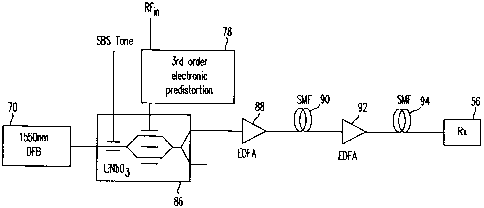
[0002] FIG. 1 shows a conventional optical (light) analog communications
system of the type
used in cable television (CATV). A 1550 nm DFB (distributed feedback) laser 70
is externally
modulated using a lithium niobate modulator 86. The laser beam is first phase
modulated by a
high frequency "SBS" tone supplied to the modulator 86 in order to suppress
Stimulated Brilloui
Scattering (SBS). The beam is then intensity modulated by the RF (radio
frequency) signal
which is the information bearing signal, such as a television signal which
includes various CATV
channels. The RF signal is predistorted by an electronic predistortion circuit
78 to compensate
for the third order non-linearities of the modulator 86. The two output
signals from modulator 86
are 180° out of phase. At the output port of the modulator, one output
signal is amplified by an
optical amplifier such as an EDFA (erbium doped fiber amplifier) and
transmitted in single mode
(SMF) optical fiber span 90, 94. One, two or more additional optical
amplifiers 92 are provided
depending on the span length. The signal is then conventionally detected at
the remote receiver
56.
[0003] In order to improve carrier to noise ratio, multi-wavelength optical
systems have been
proposed (see for instance U.S. Patent 5,940,196 PIEHLER et al. and U.S.
Patent 5,278,688
BLAUVELT et al., both incorporated herein by reference in their entireties).
In such systems the
laser beams can be combined upstream of the modulator, as shown in FIG. 2a
(from PIEHLER et
al.) or after the modulator as shown in FIG. 2b (from BLAUVELT et al.) In FIG.
2a two light
sources, typically lasers 70 and 72 (such as distributed feedback lasers),
output respectively
optical signals of wavelength A1 and ~2. These are applied via waveguides 74
and 76 to a
wavelength division multiplexer (WDM) 80 which is coupled via waveguide 82 to
a conventional
RF modulator 86. These modulated signals are then carried via the optical
fiber span 90 to
remote receiver 56 which includes a second wavelength division multiplexer 96
which outputs
CA 02478357 2004-08-20
the signals along waveguides 98 and 100 and connects them to respectively
photo detectors 104
and 108 detecting wavelengths ~~ and a2. The electrical (RF) signals output
from photo detectors
I04 and 108 are then combined in radio frequency combiner 110 to provide the
RF (CATV)
output signal.
[0004] In Fig. 2b, an RF signal source 111 drives (modulates) each of lasers
110 which are
connected in parallel so as to output, on waveguides 112, modulated optical
signals. These are
combined in optical coupler 113 and transmitted along the optical span to the
receiver end along
waveguides 114 to respectively receivers 115. In FIG. 2b the combination of
optical signals is
performed subsequent to (downstream of) the RF modulation.
[0005] The second order (CSO) distortion generated in optical fiber in a mufti-
wavelength
optical communications system is believed to include three major sources which
are respectively
self phase modulation (SPM), cmss phase modulation (XPM), and optical Ken
effect (OKE) in
conjunction with polarization dependence loss (PDL). SPM is considered to be
one of the main
technical problems in a long optical fiber scan with high launch power for a
single wavelength
transmitter. SPM is a non-linear optical phenomenon in which the optical phase
of an optical
wave varies with the intensity of the light. This non-linear phase variation
phase is given by the
formula:
(2xAZn2~ ~l'~t~ ( 1 )
where Z is the distance propagated, A the effective area (cross section) of
the optical fiber, n2 the
non-linear refractive index, A the wavelength of the light, and P the optical
power being
modulated by the RF signal as it varies with time t.
[0006] In effect, when the wave propagates through the optical fiber SPM
creates a "chirp" that
depends on the intensity of the propagated light signal. Dispersion in the
fiber then transforms
the chirp into an intensity modulation at sum and difference frequencies of
the fourier
components on the fundamental signal P(t). These new frequency components are
called the
composite second order (CSO) distortion. In digital and analog CATV networks
CSO is a
measurement of degration of signal quality.
(0007) SPM dispersion-induced CSO has been studied: see Phillips, et al., IEEE
Photonics
Technology Letters, vol. 3, p. 489 (1991 ). The second order non-linearity
introduced by the SPM
dispersion for a single wavelength transmitter is given by:
2
CA 02478357 2004-08-20
2 NL,,v,~p = _0.5 P,n (Zet1')~ ~2 k ~a, m (2 ~t' fd)2
[0008] The resulting CSO intensity is then given by:
1 2 n2
CSO = Ncso~ 2 Pin (Zet~') ~2 k Aea m (2 ~ ~)
where
Ncso is the CSO beat count
P~, is the launched optical power
~i2 is the 2nd derivative of the propagation constant (related to
the dispersion (D) by ~2= D~2/(2mc))
k=2u/awhere A, is the laser wavelength.
nz is the non-linear refractive index
m is the modulation index
Ae~ is the effective area of the fiber.
f~ is the frequency where the CSO occurs.
(Z~)2 is the square of the effective length of fiber (fiber length
corrected for the losses), if one EDFA is used just after the
transmitter, and (Ze~)2 is defined by:
(~) 2 = ~ ~ (4)
a
where L is the fiber length and a the fiber attenuation.
[0009] For an 80 channel CATV system having a SOkrn long fiber link with one
l7dBm EDFA
located just downstream of the transmitter, the CSO at 547MHz due to SPM
dispersion is about -
64dBc. If a link of 100km length is used with an additional l7dBm EDFA located
at SOkrn from
the transmitter, the CSO is about -54dBc.
[0010] Cross Phase Modulation (XPM) is similar to Self Phase Modulation (SPM),
except the
optical phase of one wavelength is modulated by the optical power of the other
wavelength.
When two optical signals propagate in the same optical fiber the non-linear
phase shift generated
by the two signals due to SPM and XPM is:
3
CA 02478357 2004-08-20
(2~rAZn2~ ~'r(t~ + bPJ(t~~ (5)
where the indices i and j refer to the signal i or j, P; and P~ are the power
of signals i and j, b is a
parameter that depends on polarization, and is equal to 2 when the
polarizations are aligned and
2/3 when the polarization are perpendicular. The first term in the second
parentheses
corresponds to SPM and the second term to XPM.
[0011] The CSO generated by the non-linear phase shift of the combined effect
of SPM and
XPM can be calculated numerically using the split-step Fourier technique (see
G. Agrawal, "Non
Linear Fiber Optic" second edition, Academic Press, or F. Coppinger, et al.,
"Proceedings,
Optical Fiber Communication, 2001, paper WCC2-1. FIG. 3 shows (see key to FIG.
3) the
calculated CSO as a function of distance when launching l6dBm into optical
fiber with only one
wavelength, two wavelengths at l6dBm each with parallel polarization, and two
wavelengths at
l6dBm with perpendicular polarization. The two wavelengths carry the same
information (i.e.,
the RF signal phase is the same for the two wavelengths). The CSO distortion
is shown for
NTSC CATV channel 78 (547.25 MHz) which is a high frequency end of the CATV RF
channel
allocation. CSO generated by SPM and XPM is worse at higher frequency
channels.
(0012] Clearly the use of two wavelengths significantly increases the CSO
distortion. In
FIG. 3, it is assumed that one of the wavelengths is delayed at the receiver
side to compensate for
the dispersion in the fiber (the delay element is not however depicted).
[0013] Another source of CSO distortion in a dual wavelength fiber link is the
above-
mentioned optical Kerr effect combined with polarization dependence loss (OKE-
PDL). The
optical Ken effect modulates the polarization of one wavelength with the
intensity of the other
wavelength, leading to intensity to polarization modulation. When there is a
polarization
dependent loss (or gain) element before the receiver, the polarization
dependence loss multiplies
the signal with itself and therefore generates distortion. OKE-PDL has been
studied in Phillips
and Ott, Journal of Lightwave Technology JLT, Vol. 17, p. 782, (1999). The CSO
distortion
generated by OKE-PDL is at a minimum if the two wavelengths are transmitted
with their two
states of polarization either parallel or perpendicular. It is at the maximum
if the polarization
difference between the two wavelengths is at 45 degrees. In this later case
the CSO distortion
would vary as a function of time as the polarization state between the two
wavelengths will vary
as a function of time due to different temperatures or mechanical stress of
the fiber. Note that the
4
CA 02478357 2004-08-20
CSO distortion generated by OKE-PDL only occurs if PDL is present in the
optical link; it is
minimized when low PDL optical components are used.
SUMMARY
[0014] The present invention is directed to a method and apparatus which
reduce CSO
distortion induced by SPM, XPM and dispersion in a multiple wavelength optical
communication
system by using a delay to launch the multiple optical (light) signals (each
having different
wavelengths) at different RF phases. Using the delay introduces an RF phase
shift proportional
to the RF frequency. In this case "phase" merely refers to the relative delay
between two signals
which are otherwise carrying the same information. If the number of
wavelengths is increased,
an incremental delay could be introduced between each wavelength.
[0015] CSO distortion generated by dual wavelength operation in an optical
system is worse
than with a single wavelength is that the non-linear optical phase shift
generated by SPM
combines positively with the optical phase shift generated by the XPM when the
two
wavelengths carry exactly the same information, e.g. in the RF domain, as in
FIGS. 2a~ 2b.
Referring to equation 5 above, if the two optical signals have identical power
levels, identical
polaristtyions-as well as the same variation with time, the optical phase
shift will be triple
compared to that of single wavelength operation. The variation is multiplied
by S/3 when the
polarizations are perpendicular.
[0016) To produce this effect therefore, in accordance with the invention the
two optical signals
are phase shifted by the equivalent 180 degrees of the highest frequency RF
signal. That is, one
of the optical signals is delayed by the equivalent of half a wavelength in
terms of the highest RF
frequency information carried by the two signals. In one embodiment at the
transmitter (or
repeater) there are two lasers outputting optical signals at two slightly
separated wavelengths.
The two optical signals are then applied to a modulator and are modulated by
the same RF input
signal, which is the information carrying signal. The modulated optical
signals are then applied
to a first wavelength division multiplexer splitting the signal into the two
wavelengths. The two
wavelengths are carried in different paths, one of which includes a delay
device such as a short
length of optical fiber providing the required delay. The two signals on their
respective paths,
one signal delayed relative to the other, are applied to the input terminals
of a second wavelength
division multiplexer which outputs on the optical fiber span the combined
signal which is
CA 02478357 2004-08-20
transmitted to the remote conventional optical receiver which conventionally
splits up the
received optical signal into the two wavelengths which are then respectfully
photo detected and
output as in FIG. 2a. In other embodiments the delay is provided in the RF
domain, that is the
RF signal is split into two paths to one of which the delay is applied and
then the signal in each of
the two paths is used to modulate one of two lasers, each operating at one of
the two respective
wavelengths.
[0017] This approach can be used either in the head end optical transmitter or
in a repeater in a
middle of a long optical fiber span. Thus in accordance with the invention a
first optical signal is
provided having a first center wavelength and a s~ond optical signal is
provided having a
second, slightly different center wavelength. Both optical signals are
modulated by the same
information signal and carried in an optical fiber span or other optical
communications channel.
The phase of the RF information in the first optical signal is delayed
relative to the phase of the
RF information in the second optical signal. When the phase shift is applied
in the middle of a
span the RF phase shift is done only in the optical domain. The actual amount
of delay is
determined theoretically or experimentally, as described in further detail
below. It has been
found that a delay of about half a wavelength of the high frequency RF channel
(typically S50
MHz) is useful; however this is not limiting.
BRIEF DESCRIPTION OF THE DRAWINGS
[0018] FIG. 1 shows a conventional optical analog communication system as used
in cable
television.
(0019] FIG. 2a shows a known two wavelength communication system which is an
improvement over that of FIG. 1.
[0020] FIG. 2b shows a second known mufti-wavelength communications system.
[0021] FIG. 3 shows a plot of transmission span distance (horizontal axis) vs.
CSO distortion in
channel 78 (vertical axis).
[0022] FIG. 4 shows an embodiment of an optical communication system in
accordance with
the invention.
[0023] FIG. S shows a plot of the delay (horizontal axis) vs. CSO distortion
(vertical axis) in
accordance with the invention.
(0024] FIG. 6 shows an optical transmitter in accordance with the invention.
6
CA 02478357 2004-08-20
[0025] FIG. 7 shows another version of an optical transmitter in accordance
with the invention.
[0026] FIG. 8 shows yet another optical transmitter in accordance with the
invention.
[0027] Similar reference numerals in various figures are intended to refer to
similar elements or
components.
DETAILED DESCRIPTION
[0028] FIG. 4 shows one embodiment of an optical system in accordance with
this invention
which is essentially the same as that of FIG. 2a, with like elements similar
labeled, but with the
addition of a delay device 118 including an additional wavelength division
multiplexer 120
connected to a third wavelength division multiplexer 126 in the transmitter
portion of the system.
These two WDMs 120, 126, in delay device 118 as shown, are connected port-to-
port by two
optical waveguides 122, 124 which are, for instance, short lengths of optical
fiber or similar
coupling components. However, the upper optical waveguide 122 is longer than
the lower one,
124 and hence is a delay element. The delay is provided by, e.g., a short
additional length of
optical fiber. The typical length of delay is for instance one nanosecond as
described above and
this can be, as shown in waveguide 122, readily provided by approximately 20
cm of
conventional optical fiber. In FIG. 4 the dual wavelength transmitter includes
the two lasers 70,
72 which are typical conventional optical sources. The output optical signals
are coupled into a
waveguide using the polarization maintaining wavelength division multiplexer
80. The two
signals are thereby combined and coupled into the conventional modulator 86
where they are
modulated by the RF input signal, which is the information bearing signal. If
at the output of the
modulator the two RF signals carried by the two wavelengths are in phase, as
described above for
FIG. 2a, this would give the maximum undesirable CSO distortion if coupled
into the fiber span.
[0029] In accordance with the method and apparatus described here, instead the
two RF signals
carried by the two optical signals are forced to be out of phase, that is one
optical signal is
delayed relative to the other. In order to do this, the two optical signals
are separated in WDM
120 and one optical signal (that on waveguide 122) is delayed relative to the
other and the two
optical signals are then recombined by the third WDM 126. Note that the
resulting RF phase
shift is frequency dependent and is greater for higher frequency. By doing so
when launched into
the main optical fiber span the CSO distortion generated by SPM, XPM and
dispersion is reduced
or suppressed. The receiver 56 of this system is the same as that in FIG. 2a.
7
CA 02478357 2004-08-20
[0030] Note that in one variant of the Figure 4 receiver 56, a single
photodiode is capable of
receiving both optical signals ~,, ~.
[0031] We have determined that the CSO distortion at any distance along the
fiber span is
dependent on the time delay (phase shift). FIG. 5 is a graph showing the
calculated (theoretical)
CSO distortion as a function of the time delay for a 50 km long optical fiber
span having a launch
power of the optical signal of 16 dBm per wavelength. The difference between
the two
wavelengths here is about 1.6 nanometers; exemplary wavelengths are 1558.98 nm
and 1560.61
nm. In this case the phase delay is provided to the signal having the shorter
of the two
wavelengths. The CSO distortion of FIG. 5 is calculated for channel 78 which
is at 547 Mhz and
assuming transmission of 80 channels of NTSC CATV as is typical in most U.S.
commercial
cable television systems. The plots in FIG. 5 are calculated for parallel
polarization for the two
wavelengths and also for perpendicular polarization of the two wavelengths, as
shown in the FIG.
key. Also shown in FIG. 5 is the measured data indicated by the vertically
extending solid
lines. The launch polarization was varied during these measurements and the
range of variation
of the CSO distortion was measured. FIG. 5 shows that the CSO distortion is
significantly
reduced using a phase delay, in this case of approximately one nanosecond.
This is the intended
result, as confirmed by both the theoretical considerations and the measured
data shown in
FIG. 5.
[0032] FIG. 6 shows another transmitter portion of an optical communications
system in
accordance with the invention using two optical transmitters 130, 132 again of
two different
wavelengths, where each transmitter is a laser plus associated conventional
components.
Transmitter 130 outputs wavelength ~1 and transmitter 132 outputs wavelength
~2; both
transmitters are modulated by an RF signal from RF source 128. The optical
signals are output
on waveguides 134, 136 to optical coupler 138 and hence to the optical fiber
span. In this case
the phase delay is introduced in the optical domain as shown in the upper
waveguide 134 path
carrying the signal of wavelength ~1. The coupler could be a 3dB combiner or
more preferably a
WDM combiner.
[0033] FIG. 7 shows a different transmitter in accordance with the invention
where the phase
delay is introduced in the electrical (RF) domain. Here the RF signal from the
RF source 128 is
applied to transmitter (laser) 130 using an RF transmission path 140 which
includes an RF delay
device. There is no such delay device present in the lower RF transmission
path 142 where the
8
CA 02478357 2004-08-20
same RF signal drives transmitter 132. An example of an RF delay device is for
instance a length
of coaxial cable or other well-known RF delay element such as a delay line. In
the optical
domain, a typical delay element is a length of optical fiber between the two
WDMs. Also, an
optical chirp grating or a length of dispersion compensating fiber can be used
as the delay device
in the optical domain to create the delay between the two wavelengths.
[0034] The methods and apparatus disclosed here can also use polarization
maintaining optical
fiber for the delay element in the optical domain. Using polarization
maintaining fiber and also
polarization maintaining wavelength division multiplexers impxoves control of
the polarization of
the optical signals and ensures that the wavelengths of the two optical
signals are launched with
either parallel or perpendicular polarization. In effect, launching the two
wavelengths with
parallel or perpendicular polarization reduces the effect of the optical Kerr
effect and polarization
dependence loss as described above. In addition, launching two wavelengths at
known
polarization enables an accurate calculation of nonlinear effects via equation
5, compared to the
case of random polarizations.
[0035] Using a time delay to achieve the desired phase shift gives a frequency
dependent phase
shift. The phase shift can also be achieved in yet another transmitter by
using the two output
signals from the optical modulator. When using two lasers 70, 72 driving one
conventional Mach
Zender external modulator 80, the modulator 80 typically provides two optical
output signals (see
FIG. 8). The RF information carried by one of the optical outputs is out of
phase by 180 degrees
with respect to the other output, i.e. one output is "RF inverted" compared to
the other.
[0036] As shown in the transmitter of FIG. 8, which is partly similar to that
of FIG. 4, the two
optical signals output from the modulator 86 are coupled to two wavelength
division multiplexers
146, 148 in order to be separated into the two optical signal wavelengths ~,
and ~2. One optical
signal, of the first wavelength, provided from one output is then combined
with the other optical
signal. The resulting optical signals contain two different wavelengths with
the RF information
phase 180° shifted between the two RF signal carried by the two optical
beams over all RF
frequencies. The FIG. 8 transmitter has been found to significantly reduce the
CSO distortion
due to XPM and SPM. Note there is no explicit delay element shown here, but
the arrangement
of the WDMs 146, 148, 150, 152 provides the phase shift, hence this
transmitter also includes a
phase shifting device. In Figure 8, the subscript "+" refers to the upper
output of the modulator
86 and "-" refers to the other output of modulator 86. Each modulator 86
output has two
9
CA 02478357 2004-08-20
wavelengths A,, ~. The RF information carried by one modulator output is 180
degrees out of
phase with the other output.
[0037] While the above description is for a system that minimizes CSO
distortion, a similar
arrangement compensates for dispersion in the optical fiber span. This allows
a wide variety of
single photodiode receivers to achieve a minimum high channel CNR (carrier to
noise ratio)
degradation due to the optical fiber dispersion. Using a system similar to
that in Figure 4, in one
example a launch power of 20dB is provided per wavelength into the optical
fiber span 90. The
RF carrier signals are delayed by delay device 118 so as to add coherently,
providing a value of,
e.g.+6dB. Noise caused by dispersion in the span 90 adds incoherently, and has
a value of, e.g.,
3dB. The delay (phase shift) supplied by the delay device advantageously
increases the CNR by
up to 3dB. If each wavelength has, e.g., l7dbm of SBS (Stimulated Brillouin
Scattering)
suppression, then the sum of the two optical signals advantageously has 20 dBm
of SBS
suppression thereby providing the desired dispersion compensation.
[0038] The invention is not limited to dual wavelength optical systems as
described above, but
is applicable to systems carrying three or more optical wavelengths. With more
than two
wavelengths, an incremental time delay is applied between the wavelengths such
that the sum of
the different RF frequency signals carried by the different wavelengths
becomes independent of
the time for high frequency channels. In the following equation, the non-
linear optical phase
shift for wavelength i in such a mufti-wavelength system is:
~,."' =(2~cAZnzl~,; P,. (t)+~bjP~(t-zi) (6)
jxi
Where P;(t) is the optical power for wavelength i, b~ is a coefficient that
depends on the
polarization of wavelength j compared to wavelength i, and T~ is the time
delay introduced
between wavelength j and wavelength i. The time delays between the wavelengths
are chosen
such that the sum in the brackets of equation 6 becomes independent of the
time. Such a system
would be an extension of that of e.g. Figure 4 with an additional third laser
source and an
additional delay device for the third optical wavelength.
[0039] This disclosure is illustrative and not limiting. Further modifications
to the invention
will be apparent to one skilled in the art in light of this disclosure and are
intended to fall within
the scope of the appended claims.