Note : Les descriptions sont présentées dans la langue officielle dans laquelle elles ont été soumises.
CA 02478573 2004-09-02
WO 02/071246 PCT/CA02/00299
1
Title of the Invention
AN APPARATUS FOR CONTROLLING ACCESS IN A DATA PROCESSOR
Field of the Invention
The present invention relates to access control in
a data processor, and in particular but not limited to
access control in a single instruction multiple data (SIMD)
processor.
Background of the Invention
A typical single-instruction-multiple-data (SIMD)
processor has multiple processor units each having its own
associated memory space. The processor units are simple
processes unable to fetch or interpret instructions, and are
controlled by a single control unit whereby the processor
units act as slaves, performing at its request, arithmetic-
logic operations. One advantage of this architecture is
that more memory and processor units can be easily added to
the computer.
An example of a SIMD processor is described in
U.S. Patent No. 5,956,274 ('274b patent) issued on 21St
September, 1999 to Duncan G. Elliott, et al. In this
architecture the processing units are placed within the
memory, there being one processor unit per column of storage
elements, each processor unit being directly coupled to the
sense amplifier of each column, and whose output is coupled
to the memory column decoder. Each processor element is a
single bit processor element and is capable of processing
serial data output from the memory column to which it is
coupled and associated. The disclosed structure allows for
higher bandwidth communications between the memory and
processing elements, allowing for a much high processing
CA 02478573 2004-09-02
WO 02/071246 PCT/CA02/00299
2
throughput as processing is not limited by the ability to
provide data to the individual processing elements.
There are however aspects to the disclosed
architecture that hamper its ability to be widely
implemented. First, the structure disclosed in the '274
patent implements a single row i.e. 1-D layout of processing
elements. Second, processing elements are coupled to and
associated with a single column of memory such that the
processing elements in the '274 patent are only able to
communicate, with the column or columns of memory with which
they are coupled and associated.
In applications such as the processing of image,
including video, it is desirable to have a high bandwidth of
data from the memory. It is further desirable to have
access to numerous portions of memory, including those with
which a given processing element is not associated. It is
also advantageous to implement an array of processing
elements i.e. a 2-D structure.
The tight integration of processing elements and
memory as outlined in the '274 patent generally makes it
difficult to provide for communications between a two
dimensional array of processing elements. It is further
difficult to provide for communications between a given
processing element and the portions of memory with which it
is not associated. A communication network that implements
1 to 1 communications links between a given processing
element and all other processing elements and all portions
of memory is not practical, even with multi-layer
metallization technology as is found in current
semiconductor processing. Therefore there is a need for a
communications between processing elements and memory
without requiring 1 to 1 links between elements and is
CA 02478573 2004-09-02
WO 02/071246 PCT/CA02/00299
3
implementable within a structure where processing elements
are integrated in memory.
Summary of the Invention
According to one aspect of the present invention,
there is provided a data processor apparatus, comprising: a
first processor element and a second processor element, a
memory having a first part and a second part, the first
processor element being coupleable to the first part for at
least one of read and write access, the second processor
element being coupleable to the second part for at least one
of read and write access, and an access switch for
selectively coupling the first processing element to one of
the first part, for at least one of read and write access
and the second part, for at least one of read and write
access.
Advantageously, this arrangement enables a
processor element to access a memory segment associated with
another processor element without the need to involve the
processor element associated with the other memory segment
in the data transfer, which therefore allows the associated
processor element to perform other functions, rather than
spend time/cycles transferring data to another processor
element from its memory segment. This arrangement not only
provides any flexibility of enabling data transfers between
different memory segments and a given processor element, but
also significantly reduces the time required for the
transfer, and in embodiments of the present invention, data
transfers from non-local memory segments may be achieved in
a single cycle.
According to another aspect of the present
invention there is provided a data processor apparatus,
comprising: a first processor element and a second processor
CA 02478573 2004-09-02
WO 02/071246 PCT/CA02/00299
4
element, a memory having a first part and a second part,
said first processor element being coupleable to said first
part for at least one of read and write access, said second
processor element being coupleable to said second part for
at least one of read and write access, and an access switch
for selectively coupling said first processing element to
one of said first part, for at least one of read and write
access, and said second part, for at least one of read and
write access.
According to another aspect of the present
invention there is provided a data processor apparatus
comprising a plurality of processor elements, a memory
having a plurality of parts, each different part being
coupleable to a different one of said plurality of processor
elements, and switch means for switch/coupling at least one
of said processor elements from its associated memory part
to the memory part associated with at least one other
processing element.
According to another aspect of the present
invention there is provided a switching element for
switchably coupling an array of circuit elements each having
an input and an output, the switching element comprising: an
input for coupling to the output of a circuit element, an
output for coupling to an input of a circuit element, and
first and second switch means, said first switch means
having a first state in which said first port is coupled to
said input port, and a second state in which said first port
is coupled to said output port, and said second switch means
having a first state in which said second port is coupled to
said input port and a second state in which said second port
is coupled to said output port.
CA 02478573 2004-09-02
WO 02/071246 PCT/CA02/00299
According to another aspect of the present
invention there is provided a data processor apparatus
comprising a plurality of processor elements and a memory
having a plurality of segments, each containing at least one
5 column of storage elements, and each segment having a memory
port, and wherein at least one memory port is coupled to at
least two processor elements.
According to another aspect of the present
inventions there is provided a data processor having a first
memory block, a first array of processor elements, each
processor element being capable of accessing said first
memory block, a first array of switching elements each
associated with a respective processor element of said first
array, a second memory block and a second array of processor
elements, each being capable of accessing said second memory
block, a second array of switching elements each associated
with a respective processor element of said second array,
wherein a corresponding switching element of said first
array is coupled to a corresponding switching element of
said second array.
According to another aspect of the present
invention, there is provided a data processor comprising an
array of circuit elements and a switching element associated
with each of said circuit elements said switching elements
being interconnected to enable data to be transferred
between said circuit elements.
Brief Description of the Drawings
Examples of embodiments of the present invention
will now be described with reference to the drawings, in
which: -
CA 02478573 2004-09-02
WO 02/071246 PCT/CA02/00299
6
Figure 1 shows a block diagram of a data processor
according to an embodiment of the present invention;
Figure 2 shows a diagram of an access switching
arrangement according to an embodiment of the present
invention;
Figure 3 shows a schematic diagram of a data
processor apparatus according to an embodiment of the
present invention;
Figure 4 shows a schematic diagram of a
computational unit according to an embodiment of the present
invention;
Figure 5 shows a schematic diagram of a switching
element interconnect scheme according to an embodiment of
the present invention;
Figure 6 shows a diagram of an array of
computational units according to an embodiment of the
present invention;
Figure 7 shows a diagram of a two-dimensional
array of switching elements and an interconnect scheme
according to an embodiment of the present invention;
Figure 8 shows an embodiment of a switching
element, which may be used in the interconnect scheme of
Figure 7;
Figure 9 shows a diagram of a switching element,
according to another embodiment of the present invention;
Figure 10 shows an array of interconnected
switching elements of the embodiment shown in Figure 8;
CA 02478573 2004-09-02
WO 02/071246 PCT/CA02/00299
7
Figure 11 shows a diagram of a switching element
according to another embodiment of the present invention;
Figure 12 shows a diagram of an array of switching
elements of the embodiment of Figure 10;
Figure 13 shows a diagram of a switching element
according to another embodiment of the present invention;
Figure 14 shows Table 1, which contains the
possible states of a tri-stateable inverter;
Figure 15 shows Table 2, which contains examples
of various sets of control signals for controlling the
embodiment of the switching element shown in Figure 13;
Figure 16 shows a diagram of a switching element
according to another embodiment of the present invention;
Figure 17 shows a diagram of a switching element
according to another embodiment of the present invention;
Figure 18 shows a diagram of a switching element
according to another embodiment of the present invention;
Figure 19 shows a diagram of a switching element
according to another element of the present invention;
Figure 20 shows a block diagram of a data
processor according to an embodiment of the present
invention;
Figure 21 shows a diagram of a data processor
according to another embodiment of the present invention;
Figure 22 shows a diagram of a switching element
according to an embodiment of the present invention;
CA 02478573 2004-09-02
WO 02/071246 PCT/CA02/00299
8
Figure 23 shows a block diagram of a data
processor according to another embodiment of the present
invention, and
Figure 24 shows a data processor according to
another embodiment of the present invention.
Description of Embodiments
Embodiments of the current invention present
aspects of a communications network that allows for
communications between a given processing element and other
processing elements, as may be found in a processor that
implements a plurality of SIMD processing elements, and
between a given processor and various regions of memory.
Referring to Figure 1, a data processor 1,
according to an embodiment of the present invention,
comprises a plurality of processor elements (PE) 3, 5, 7 and
a memory 9, which may for example comprise a random access
memory (RAM). The memory includes a plurality of segments
11, 13, 15 and each segment has an associated input/output
port 17, 19, 21 to permit read/write access to a respective
memory segment. Each memory segment may comprise a one
dimensional array (e. g. a column) or a two-dimensional array
(e.g. containing a plurality of rows and columns) of one bit
memory or storage elements. The memory may include a row
selector to select a particular row of memory elements and
each segment may include a column selector to select a
particular column of memory elements and to connect that
column to the I/O port, if each segment contains more than
one column of memory elements.
The data processor 1 further includes a plurality
of switching elements (SE) 23, 25, 27. The first switching
element 23 is coupled to the I/O ports 17, 19 of the first
CA 02478573 2004-09-02
WO 02/071246 PCT/CA02/00299
9
and second memory segments 11, 13 and is switchable to
selectively couple one of the first and second memory
segments 11, 13 to the first processor element 3.
Similarly, the second switching element 25 is coupled to the
I/O ports 19, 21 of the second and third memory segments 13,
and is arranged to selectively couple either the second
or third memory segment 13, 15 to the second processor
element 5. The third switching element 27 is coupled to the
third memory segment 15 and possibly to a fourth memory
10 segment (not shown) and may be arranged to selectively
couple the third memory segment 15 or the fourth memory
segment to the third processor element 7. The first
switching element 23 may be arranged to provide at least one
of read access by the first (i.e. its local) processor
15 element to at least one of the first (i.e. its local) memory
segment 11 and to the second (i.e. its remote, e.g.
neighbouring or more remote than neighbouring) memory
segment 13, and write access from the first processor
element 3 to at least one of the first and second memory
segments 11, 13. Similarly, the second and/or third
switching elements 25, 27 may be arranged to provide at
least one of read access to at least one of its local and
remote memory, and write access from the processor element
to at least one of its respective local and remote memories.
The switching of each switching element 23, 25, 27 may be
controlled by applying a control signal to a respective
control signal input port 29, 31, 33.
Advantageously, the switching arrangement shown in
Figure 1, allows each processor element direct access not
only to its local memory segment but also to the local
memory segment of another processor element. This enables
each processor element to perform calculations based on data
contained in its local and associated remote memory
CA 02478573 2004-09-02
WO 02/071246 PCT/CA02/00299
segments. For example, in one embodiment, each processing
element includes first and second local registers for
storing data from its local memory and data from its
associated remote memory, respectively, and an arithmetic
5 logic unit (ALU) for performing a calculation based on the
contents of these registers. This arrangement is
particularly beneficial for image processing, where a
comparison is made between the value of one pixel and that
of another pixel, for example a neighbouring pixel for
10 motion estimation and/or data compression.
In one embodiment, each of the switching elements
may be controlled to provide the same memory segment to
processor element coupling at the same time. For example,
each switching element may first be controlled to couple
each processor element to its local memory segment for read
access. Secondly, each switching element may be controlled
to couple each processor element to its respective remote or
neighbouring memory segment for read access. Thirdly, each
processor element may be controlled to perform an operation
based on the data from its local and associated remote
memory segment and subsequently to output the result of the
operation. Each switching element may then be controlled to
write the result of the operation into either its local or
remote memory segment. Advantageously, controlling all of
the switching elements to perform the same switching
operation avoids memory segment and processor element access
conflicts and enables all of the switching elements to be
controlled simultaneously by the same control signal or
instruction. This form of processing is particularly
applicable to digital image processing and allows image
pixels to be processed in parallel.
The embodiment shown in Figure 1, illustrates an
example of a switching arrangement in which each processor
CA 02478573 2004-09-02
WO 02/071246 PCT/CA02/00299
11
element has access either to its local memory segment or to
the memory segment to its right (i.e. East). In another
embodiment, each switching element may be arranged to
provide each processor element access to its local memory
segment or to a remote memory segment to its left (i.e.
West). In a further embodiment, each switching element may
be arranged to permit each processor element selective
access to either its local memory segment, a remote (e. g.
neighbouring) memory segment to its right (East), or to a
remote (e. g. neighbouring) memory segment to its left
(West). An example of such a switching arrangement is shown
in Figure 2.
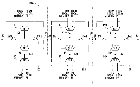
Referring to Figure 2, the switching arrangement
101 according to an embodiment of the present invention,
comprises a plurality of switching elements 103, 105, 107.
Each switching element includes a first port 109, 111, 113,
which is coupled to the output of a selector switch (SL1),
which selectively couples the first port either to the local
memory (segment) associated with each switching element or
the local processor element associated with each switching
element, the switching being controlled by a control signal
applied to a control signal input port 115, 117, 119. Each
switching element further comprises a second port 121, 123,
125 (located to the left, or west, of each switching element
in this embodiment), and a third port 127, 129, 131
(situated to the right or east of each switching element, in
this embodiment). The east port 127 of the first switching
element 103 is coupled to the west port 123 of the second
switching element 105, and the east port 129 of the second
switching element 105 is coupled to the west port 125 of the
third switching element 107. Each switching element 103,
105, 107 further includes first and second switches SW1,
SW2, the first switch SW1 being arranged to couple/de-couple
CA 02478573 2004-09-02
WO 02/071246 PCT/CA02/00299
12
the first port 109, 111, 113 of each switching element to
the west port 121, 123, 125, and the second switch SW2 being
arranged to couple/de-couple the first port 109 to the east
port 127, 129, 131 of each switching element.
Each switching element 103, 105, 107 further
includes a second switch selector SL2 connected to each of
the first, second and third ports of each switching element,
and which is arranged to selectively couple one of the
first, second and third ports to a fourth port 133, 135,
137, under the control of a control signal applied to its
control signal input port 139, 141, 143. Each of the fourth
ports 133, 135, 137 are coupled to a third selector switch
SL3 for selectively switching the output from the second
selector switch either to the local memory associated with
the switching element or to the local processor element
associated with the switching element. Switching of each
selector switch SL3 is controlled by a control signal
applied to its control signal input port 145, 147, 149.
The switching arrangement 101 shown in Figure 2 is
configurable to permit data transfer between local memory
and local processor element, or between the local memory or
local processor element associated with one switching
element and the local memory or local processor element
associated with a neighbouring switching element to which it
is coupled. Examples of various modes of operation of the
switching element 101 will now be described.
According to a first mode of operation each
switching element is configured to permit its local
processor element to read from its local memory. In this
mode, selector switch SL1 is controlled to couple each of
the first ports 109, 111, 113 to a respective local memory,
switches SW1 and SW2 are both open (as shown), the second
CA 02478573 2004-09-02
WO 02/071246 PCT/CA02/00299
13
selector switch SL2 is controlled to couple the first port
109, 111, 113 to the fourth port 133, 135, 137, and the
third selector switch SL3 is controlled to couple the fourth
port 133, 135, 137 to the local processor element.
In a second mode of operation, each switching
element is configured to write from its local processor
element to its local memory, in which case the first
selector switch SL1 is controlled to couple the output of
its local processor element to the first port 109, 111, 113,
the first and second switches SW1, SW2 are both open, the
second selector switch SL2 is controlled to couple the first
port 109, 111, 113 to the fourth port 133, 135, 137, and the
third selector switch SL3 is controlled to couple the fourth
port 133, 135, 137 to the local memory.
In a third mode of operation, each switching
element is configured to transfer data from its local memory
to the local processor element of the switching element to
its right (east). In this mode, the first switching element
SL1 is controlled to couple the first port 109, 111, 113 to
the local memory, the first switch SW1 of each switching
element is open, the second switch SW2 of each switching
element is closed to connect the first port 109, 111, 113 to
a respective east port 127, 129, 131, the second selector
switch SL2 is controlled to couple a respective west port
121, 123, 125 to the fourth port 133, 135, 137. In this
configuration, the first port 109, 111, 113 of each
switching element is connected to the fourth port 135, 137
of the neighbouring switching element to its right.
Finally, the third switch selector SL3 is controlled to
couple the fourth port 133, 135, 137 to its local processor
element.
CA 02478573 2004-09-02
WO 02/071246 PCT/CA02/00299
14
In another mode of operation, each switching
element is configured to write from its local processor
element into the local memory associated with a switching
element to its right (east). In this case, each switching
element is configured in a similar way to that described
immediately above in connection with a memory read access,
except that the first selector switch SL1 is controlled to
couple the local PE to the first port 109, 111, 113, and the
third selector switch SL3 is controlled to couple the fourth
port 133, 135, 137 to the local memory.
In another mode of operation, each switching
element is configured to transfer data from its local memory
to a processor element associated with a switching element
to its left (west). In this mode, each first selector
switch SLl is controlled to couple the first port 109, 111,
113 to the local memory, the first switch SW1 is closed to
couple the first port 109, 111, 113 to the left port 121,
123, 125, and the second switch SW2 is open. The second
selector switch SL2 is controlled to couple the right port
127, 129, 131 of each switching element to the fourth port
133, 135, 137, so that the first port of each switching
element is effectively coupled to the fourth port of the
switching element to its left. Finally, the third selector
switch SL3 is controlled to couple the fourth port 133 to
the local processor element.
In another mode of operation, each switching
element may be configured to write the output of its local
processor element to the local memory associated with the
switching element to its left (west). This mode is similar
to that described immediately above in connection with a
west read access, except that the first selector switch SL1
is controlled to couple the first port 109, 111, 113 to the
output of its local processor element, and the third
CA 02478573 2004-09-02
WO 02/071246 PCT/CA02/00299
1S
selector switch SL3 is controlled to couple the fourth port
133, 135, 137 to its local memory.
In each of the switching modes described above,
each switching element has the same configuration, and
therefore conveniently, the same set of control signals can
be applied to the switches SW1, SW2 and the selector
switches SL1, SL2, SL3 of each switching element.
Therefore, the control lines for corresponding switches and
selector switches can be connected together, substantially
simplifying and reducing the number of control wires which
would otherwise be required if each element was controlled
independently of the others.
Any number of switching elements may be used to
transfer data between any number of processor elements or
1S their respective memory segments. Generally, one switching
element is required for each processor element.
Byte-Wise Processing and Data Transfer
In one embodiment, each processor element is
capable of processing a single bit, and a plurality of
processor elements may be functionally grouped together to
process a multiple bit word, for example, a byte (8 bits).
A group of processor elements which function to operate on a
multiple bit word will be referred to as a computational
unit (CU) .
Figure 3 shows an example of a data processor
having a plurality of computational units, and a switching
arrangement which allows the transfer of multiple bit words
between computational units and/or between computational
units and the local memories associated with other
computational units (and optionally between memory
segments) .
CA 02478573 2004-09-02
WO 02/071246 PCT/CA02/00299
16
Referring to Figure 3, the data processor 201
comprises a plurality of computational units (CU) 203, a
memory block 205 and a plurality of groups of switching
elements (SEs) 207. In this embodiment, the computational
units are arranged in a two-dimensional array having two
rows, row 1 and row 2 and n columns. Each computational
unit has 8 processor elements allowing the computational
unit to perform byte processing, and an associated group of
switching elements 207, each containing 8 switching
elements, one switching element for each processor element.
This configuration is shown in Figure 4, in which a
computational unit 203 includes 8 processing units 211, each
connected to a switching element 213. Returning to Figure
3, each computational unit 203 has 8 memory I/O ports
associated therewith, one for each processor element of the
computational unit, and in which a respective I/O port is
coupleable to a respective processor element through a
respective switching element. Thus, in this embodiment,
each 8 bit computational unit is pitch-matched to the I/O
ports of the memory. In the arrangement shown in Figure 3,
the first set of 8 I/O ports 210 and each alternate set of 8
I/O ports is associated with a successive computational unit
203 in the first row, and the second set of 8 I/O ports 212
and each alternate set of 8 I/O ports is associated with
each successive computational unit in the second row.
Each group of 8 switching elements 207 is
connected to an adjacent group of switching elements to
allow byte transfer of data from one group to an adjacent
group, as shown in Figure 5.
Referring to Figure 5, four groups of switching
elements 215, 217, 219, 221 are shown, in which the first
two groups 215, 217 occupy a first row 223 and the third and
fourth groups 219, 221 occupy a second row 225. Each group
CA 02478573 2004-09-02
WO 02/071246 PCT/CA02/00299
17
contains eight switching elements labelled 0 to 7. Each
group has an associated computational unit and an associated
local memory (not shown), wherein each local memory is
capable of storing at least one byte of data (containing 8
bits), and each computational unit is capable of byte-wise
processing.
In order to perform byte-wise transfer between a
computational unit or local memory associated with one group
of switching elements and a computational unit or local
memory associated with an adjacent group of switching
elements, each switching element of one group is connected
to a switching element of the adjacent group which has a
corresponding bit significance. Thus, as shown in Figure 5,
switching element 0 of the first group 215 is directly
connected to switching element 0 of the second, adjacent
group 217 (when position 0 may correspond to the least
significant bit (LSB)). Similarly, each of the other
switching elements 1 to 7 of the first group 215 is
connected to a corresponding switching element 1 to 7 of the
second group 217 (where position 7 may correspond to the
most significant bit (MSB)). These connections allow east-
west or west-east byte-wise transfer between the local
memory or computational unit associated with the first group
of switching elements 215 and the second group of switching
elements 217. The switching elements of the third and
fourth groups 211, 221 are connected in like manner to
permit east to west or west to east byte-wise transfer
between the computational unit or local memory associated
with the third group of switching elements 219 and the
computational unit or local memory associated with the
fourth group of switching elements 221.
In the embodiment shown in Figure 5, the first and
third group of switching elements 215, 219 are also
CA 02478573 2004-09-02
WO 02/071246 PCT/CA02/00299
18
connected to permit north-south or south-north byte-wise
transfer between the computational unit or local memory
associated with the first group of switching elements 215
and the computational unit or local memory associated with
the third computational unit 219. To permit this byte-wise
transfer, each switching element associated with the first
group 215 is connected to a switching element of the third
group 219 which has corresponding bit significance. Thus,
the switching element 0 of the first group 215 is directly
connected to the switching element 0 of the third group 219,
and each of the other switching elements 1 to 7 of the first
group 215 is directly connected to a corresponding switching
element 1 to 7 of the third group, as shown by the arrows
224. The second and fourth groups of switching elements
217, 221 are also coupled to permit north to south and south
to north byte-wise transfer between the computational unit
or local memory associated with the second group of
switching elements 217 and the computational unit or local
memory associated with the fourth group of switching
elements 221. Again, to enable this byte-wise transfer,
each of the switching elements of the second group 217 is
connected to a switching element of the fourth group 221
having the same bit significance. Thus, the switching
element 0 of the second group 217 is directly coupled to the
switching element 0 of the fourth group 221 and each of the
other switching elements 1 to 7 of the second group 217 is
directly coupled to a corresponding switching element 1 to 7
of the fourth group 221, as shown by the arrows 226.
It can be seen from the embodiment shown in Figure
5, that the switching arrangement allows byte-wise transfer
between the computational unit or local memory associated
with one group of switching elements and the computational
unit or local memory associated with an adjacent group of
CA 02478573 2004-09-02
WO 02/071246 PCT/CA02/00299
19
switching elements displaced in the east/west direction and
a group of switching elements displaced in the north/south
direction. The array of groups of switching elements can be
extended limitlessly to any size of array so that byte-wise
data transfer can be permitted between a computational unit
and/or local memory associated with any group of switching
elements and the computational unit and/or local memory
associated with any other adjacent switching element in the
same row or the same column. This arrangement is
particularly advantageous in video image processing as it
allows a pixel, which is typically described by an 8 bit
word to be compared with each of its north, south, east and
west neighbours, and each comparison can be performed for
all pixels in parallel. Thus, for example, one parallel
operation may involve the transfer of a byte of data from
the memory associated with each group of switching elements
to the computational unit associated with its adjacent
southern neighbour, for comparison with a byte stored in the
memory of its southern neighbour. Another parallel
operation may involve the transfer of a byte from a local
memory associated with each group of switching elements into
the computational unit associated with its immediate
northern neighbour for comparison with a byte stored in the
memory associated with. its northern neighbour. Other
parallel operations including for example east and west
byte-wise transfers may also be performed. In addition to
performing north to south (or south to north) and east to
west (or west to east) byte-wise transfers, it may also be ,
desirable to perform byte-wise transfers between
neighbouring groups of switching elements on the diagonal.
An example of a two dimensional array of computational units
in which byte-wise transfers between a computational unit
and its nearest eight neighbours is shown in Figure 6.
CA 02478573 2004-09-02
WO 02/071246 PCT/CA02/00299
Figure 6 shows a two-dimensional, three-by-three
array 251 of nine computational units, in which the central
computational unit 253 has 8 nearest neighbours, which
include its adjacent computational units 255 to the north
5 and 257 to the south in the same column, its adjacent
computational units 259, to the west, and 261 to the east in
the same row, and its immediately adjacent computational
units 263 to the north-west and 265 to the south-east on one
diagonal, and its immediately adjacent computational units
10 267 to the north-east and 269 to the south-west, on the
other diagonal. Tn order to permit data transfer between
the central computational unit 253 or its local memory and
the computational unit or local memory of each of its 8
nearest neighbours, each computational unit and local memory
15 has an associated switching element. In one embodiment, the
switching element associated with the central computational
unit 253 may be connected to each of the switching elements
associated with each of its nearest neighbours and each
switching element may have 8 input-output ports or buses
20 extending therefrom to connect to each of its neighbours, as
shown schematically by the arrows 271 in Figure 6. An
example of an interconnect scheme in which each switching
element is connected to each of its nearest neighbours by
one of eight buses, is shown in Figure 7. Figure 7,shows a
two-dimensional, three-by-three array 273 of switching
elements 275, in which each switching element has 8 ports or
buses 277 extending therefrom for connecting to each of its
nearest neighbour switching elements (for example to a bus
or port of each element).
Figure 8 shows an embodiment of a switching
element which may be implemented in the interconnect scheme
of the embodiment shown in Figure 7. The switching element
comprises a first multiplexer 240 having nine inputs 242 and.
CA 02478573 2004-09-02
WO 02/071246 PCT/CA02/00299
21
an output 244. Eight of the inputs are for coupling to
neighbouring switching elements and the remaining input is
for coupling to the local unit, for example a memory or
processor element output. The switching element further
includes a second multiplexes 246 having a first input 248
coupled to an output port of the local PE, and a second
input port 250 for receiving data from the local unit, e.g.
the local memory. The output of the second multiplexes is
broadcast to other switching elements. The switching
element further includes a third multiplexes having a first
input connected to the output of the first multiplexes, and
a second input coupled to an output of the local processor
element. The output of the third multiplexes is coupled to
the local memory input.
An embodiment of a switching arrangement which
advantageously allows the number of buses to be reduced,
while still retaining the connectivity of a local memory
and/or processor element to its nearest 8 neighbours will
now be described below. Referring to Figure 9, a switching
element 301 has four input/outputs 303, 305, 307, 309. In
this embodiment, the first and third output ports 303, 307
lie on a first north to south axis and the second fourth
input/output port 305, 309 lie on a transverse axis, which
in this embodiment is a substantially orthogonal, east to
west axis which enables other similar switching elements to
be connected to each of the input/output ports in a two-
dimensional grid pattern (which will be described below),
although other arrangements are also possible.
The switching element 301 further includes four
switches 311, 313, 315, 317, the first switch 311 being
connected to the first input/port 303, the second. switch 313
being connected to the second input/output port 305, the
third switch 315 being connected to the third input/output
CA 02478573 2004-09-02
WO 02/071246 PCT/CA02/00299
22
port 307 and the fourth switch 317 being connected to the
fourth input/output port 309. Each switch is switchable
between three terminals 319, 321, 323, and further includes
at least one neutral position in which the switch is not
connected to any of the three terminals. The switching
element 301 further includes an input port 325 which is
connected to each middle terminal 321 of the four switches.
Each one of the other two terminals of each switch is
connected to the terminal of an orthogonal switch on the
same side. Thus, the first terminal 319 associated with the
first switch 311 is connected to the third terminal 323 of
the fourth switch 317. The third terminal 323 associated
with the first switch 311 is connected to the first terminal
319 of the second switch 313. Similarly, the first terminal
319 of the third switch 315 is connected to the third
terminal 323 of the second switch 313, and the third
terminal 323 of the third switch 315 is connected to the
first terminal 319 of the fourth switch 317.
The switching element further includes an output
selector switch 327 having four inputs A, B, C and D and an
output 329. A respective one of the four inputs A, B, C and
D is connected to a respective one of the interconnected
switch terminal couples 319, 323 also labelled A, B, C and D
(although these interconnections are not shown for clarity).
This embodiment further includes a second selector switch
341 having two inputs 343, 345 and an output 347. The first
input 343 is connected to the output 329 of the first
selector switch 327 and the second input 345 is connected to
the input port 325 of the switching element (although this
connection is also not shown for clarity).
The switching element 301 is capable of directing
data received at the input 325 either to local elements
(e. g. local memory or local processor element) associated
CA 02478573 2004-09-02
WO 02/071246 PCT/CA02/00299
23
with the switching element, or to one of the four
input/output ports 303, 305, 307, 309. The input port 325
may be coupled to receive data from its associated local
memory, or the output of its associated local processor
element, and a switch may be provided to selectively couple
the input port 325 to one of the associated local memory and
an output of the associated processor element.
The switching element 301 is also capable of
directing data received at any one of its four input/output
ports 303, 305, 307, 309 to the output port 329 of the first
selector switch 327 and to the second output port 347 of the
second selector switch 341, depending on its state. The
switching element is also capable of transferring data
received at the input port 325 to the output port of the
second selector switch 347 again depending on its state. In
one embodiment, the output 347 of the second selector switch
341 is connected to the input of the local processor element
associated with the switching element 301. Thus, in one
mode of operation, the switching element is capable of
transferring data received at its input 325 to its output
347, for example to enable the transfer of data from its
local memory to its local processor element. In another
mode of operation, the switching element is capable of
transferring data received at any one of the four
input/output ports to its associated local processor
element. Examples of the various possible operating modes
of the switching element 301 will now be described below.
To perform a data transfer to the south, the third
switch 315 is controlled to couple the input port 325 to the
third (south) input/output port 307 so that data from the
local unit (e.g. local memory or local processor) is
transferred to the south port 307. At the same time, the
first switch 311 is controlled to couple the first (north)
CA 02478573 2004-09-02
WO 02/071246 PCT/CA02/00299
24
input/output port 303 either to its first terminal 319 or to
its third terminal 323, thereby coupling the north port 303
either to the first input A or the second input B of the
first selector switch 327. The second selector switch 327
is controlled to couple the input port to which the first
switch 311 is connected, to the output port 329. The second
selector switch 341 is controlled to connect its first input
port 343 to the output port 347, which is connected to an
input of the local unit (e. g. memory or local processor)
associated with the switching element 301. Thus, in this
mode of operation, the switching element is configured to
transfer data from the local unit to the south port 307 and
to transfer data into the local unit via the north port 303.
In another mode of operation, the switching
element 301 may be controlled to transfer locally derived
data to its north neighbour and simultaneously to receive
data derived from its southern neighbour. In this mode, the
first switch 311 is controlled to connect the north
input/output 303 to the input port 325 of the switching
element 301, and the third switch 315 is controlled to
connect the south port 307 to one of the first and third
terminals 319, 323 associated with the third switch 315, to
connect the south port 307 to one of the third or fourth
inputs C, D of the first selector switch 327, and the second
selector switch is controlled to output the data to the
local unit.
In another mode of operation, the switching
element may be configured to transfer locally derived data
to its east neighbour and to receive data from its west
neighbour. In this mode of operation, the second switch 313
is controlled to couple the input 325 of the switching
element 301 to the east port 305, and the fourth switch 317
is controlled to connect the west port 309 to one of the
CA 02478573 2004-09-02
WO 02/071246 PCT/CA02/00299
first or third terminals 319, 323 associated with the fourth
switch 317 to couple the west port 309 to one of the first
and third input ports A, C of the first selector switch 327.
The first selector switch 327 is controlled to connect the
5 appropriate input port A, C to its output port 329 and the
selector switch 341 is appropriately controlled to output
the data received at the west port 309 to the local unit.
In a fourth mode of operation, the selector switch
301 is configured to transfer data to its west neighbour and
10 to receive data from its east neighbour. In this mode, the
fourth switch 317 is controlled to couple the input port 325
of the switching element 301 to the west port 309, and the
second switch 313 is controlled to couple the east port'305
to one of the first and third terminals 319, 323 associated
15 with the second switch 313, so that the east port 305 is
coupled to one of the second and fourth inputs B, D of the
first selector switch 327. The first and second selector
switches 327, 341 are appropriately controlled so that data
received at the east port 305 is transferred to an input of
20 the local unit (e. g. local memory or local processor.
element).
In each of the modes described above for a north
to south, south to north, east to west and west to east
transfer, the switching element 301 assumes both an output
25 mode for transferring data out from one of its north, south,
east or west ports and an input mode for receiving data at
the respective opposite port. The switching element 301 can
also be configured to operate in any one of four further
modes to allow the transfer of data received at any one of
its input/output ports 303, 305, 307, 309 to an adjacent
orthogonal input/output port 303, 305, 307, 309 for
transferring data between diagonally disposed nearest
neighbours. To perform a diagonal data transfer, each
CA 02478573 2004-09-02
WO 02/071246 PCT/CA02/00299
26
switching element 301 is configured to operate in an input
mode, for receiving data at one of its input/output ports
303, 305, 307, 309 and transferring the received data to the
local unit, an orthogonal output mode, in which locally
derived data is output at a port which is orthogonal to the
input/output port established for the input mode, and a by-
pass or pass-through mode, in which the other two adjacent
orthogonal input/output ports are interconnected to allow
the transfer of data received at one of these ports to the
other remaining port. The switching element 301 is capable
of adopting all three modes simultaneously to enable
diagonal (e. g. NE, NW, SE, SW) nearest neighbour or more
remote diagonal data transfers.
An example of how switching elements may be
configured to enable a diagonal data transfer will now be
described with reference to Figure 10.
Figure 10 shows an array of three switching
elements 351, 353, 355, each of which is similar to the
switching element 301 shown in Figure 9, and like parts are
designated by the same reference numerals. The switching
elements are interconnected such that the east input/output
port 305 of the first switching element 351 is connected to
the west input/output port 309 of the second switching
element 353, and the north input/output 303 of the second
switching element 353 is connected to the south input/output
port 307 of the third switching element 355. Thus, the
second switching element 351 constitutes the east neighbour
(which may or may not be the nearest east neighbour) to the
first switching element 351, and the third switching element
355 constitutes the Northeast neighbour (which may or may
not be the nearest Northeast neighbour) to the first
switching element 351. It is to be noted that the array of
three switching elements shown in Figure 10 may be part of a
CA 02478573 2004-09-02
WO 02/071246 PCT/CA02/00299
27
larger array of switching elements and that Figure 10 simply
serves to illustrate an arrangement of switching elements
which enable a transfer between one switching element and
another switching element on its Northeast diagonal.
To perform a transfer of data locally derived at
the third switching element 355 to the first switching
element 351, the third switching element 355 assumes an
output mode, in which the third switch 315 is controlled to
connect the input port 325 of the third switching element
355 to its third (south) input/output port 307, so that
locally derived data is transferred onto the output port
307. The second switching element 353 assumes a pass-
through mode, in which the first switch 311 is connected to
its associated first terminal 319, and the fourth switch 317
of the second switching element 353 is connected to its
associated third terminal 309, thereby connecting the first
(north) input/output port 303 of the second switching
element to its fourth (west) input/output port 309. The
first switching element 351 assumes an input mode, in which
the second switch 313 of the first switching element 351 is
controlled to connect the second (east) input/output port
305 to the third terminal 323 associated with its second
switch 313 so that the east input/output port 305 is
connected to the fourth input port D of the selector switch
327. The selector switch 327 is controlled to connect the
fourth input D to its output port 329 (not labelled on
Figure 10). Thus, it can be seen that the first, second and
third switching elements are configured to provide a
continuous path from the input port 325 of the third
switching element 355 to the output port 329 of the first
switching element 351.
It is to be noted in this operating mode that each
of the switching elements 351, 353, 355 may all assume the
CA 02478573 2004-09-02
WO 02/071246 PCT/CA02/00299
ti
same three operating modes: output mode, pass-through mode
and input mode, so that each switching element assumes an
output mode in which a respective input port 325 is
connected to a respective south port 307, a pass-through
mode, in which the first and fourth switches are controlled
to couple a respective north port 303 to a respective west
port 309, and an input mode, in which a respective east port
305 is connected to a respective output port 329. This
symmetrical configuration of all of the switching elements
allows same direction, parallel, diagonal transfers between
diagonally disposed switching elements in the array. Since
each switching element is configured in the same way to
perform a given diagonal transfer, all of the switching
elements may be configured by the same set of control
signals, which enables the control of data transfers between
the switching elements to be considerably simplified.
Advantageously, as each switching element is
designed to enable data to be transferred from any of its
input/output ports to either of its adjacent, orthogonal
input/output ports, an effective diagonal data transfer can
be performed using the same buses which are used for north-
south and east-west data transfers, thereby obviating the
need for additional diagonal buses between diagonally
disposed switching elements. Thus, the switching elements
allow data transfer between a given switching element and
its nearest eight neighbours using only four buses rather
than eight, thereby considerably simplifying and reducing
the cost and complexity of the additional interconnects,
which would otherwise be required. This arrangement also
alleviates the problem of superimposing or combining a
diagonal interconnect system to a "Manhattan geometry", in
which the interconnect wires are drawn orthogonally, i.e. in
the north, south, east and west directions.
CA 02478573 2004-09-02
WO 02/071246 PCT/CA02/00299
29
In the embodiments of the switching elements shown
in Figures 9 and 10, each input mode from any of the
input/output ports 303, 305, 309, 311 has two possible
configurations. The first configuration is illustrated in
Figure 10, in which for the input mode associated with the
transfer of data into the switching element from the east
input/output port 305, the second switch 313 is connected to
the third terminal 323 associated with the second switch, so
that the east input/output port is connected to the fourth
port D of the selector switch 327. In the alternative
configuration of this input mode, the second switch 313 may
be controlled to couple to the first terminal 319 associated
with the second switch 313 so that the east input/output 305
is connected to the second input port B of the selector
switch 327, in which case the selector switch is controlled
to connect the second input port B to its output port 329.
The embodiments of the switching elements shown in
Figures 9 and 10 allow any diagonal transfer to be performed
via all possible routes. In the case of a transfer to a
switching element from a Northeast neighbour, one route is
to pass the data via its east neighbour, as shown in Figure
10, and the second route is to pass the data via its north
neighbour, for example north neighbour 357 shown
schematically in Figure 10.
In another embodiment, each of the switching
elements may be simplified to permit a diagonal transfer
using only one of these two possible routes. An example of
another embodiment of a switching element is shown in Figure
11, and an example of an array of such switching elements is
shown in Figure 12. The switching element shown in Figure
11 is similar to that shown in Figure 9, and like parts are
designated by the same reference numerals. The switching
element 301 comprises four input/output ports 303, 305, 307,
CA 02478573 2004-09-02
WO 02/071246 PCT/CA02/00299
309 having associated switches 311, 313, 315, 317. Each
switch has first and second terminals 319, 321, the first
terminal 319 (also labelled N, E, S and W) being connected
to a respective one of four input terminals, also labelled
5 N, E, S, W of a first selector switch 327. The first
terminal 319 associated with each switch is also connected
to the input/output port connected to its adjacent switch
displaced in the clockwise sense. Thus, the first terminal
319 associated with the first switch (connected to the first
10 (north) input/output port 303) is connected to the second
(east) input/output port 305, the first terminal 319
associated with the second switch 313 is connected to the
third (south) input/output port 307, the first terminal 319
associated with the third switch 315 is connected to the
15 fourth (west) input/output port 309, and the first terminal
319 of the fourth switch 317 is connected to the first
(north) input/output port 303. The second terminal 321 of
each switch is connected to the input port 325 of the
switching element.
20 Each switch is switchable between its associated
first and second terminals 319, 321, and a third, neutral or
floating state (e.g. between the two terminals), as shown in
Figure 11.
Figure 12 shows an array of four switching
25 elements of the kind shown in Figure 11 and will be used to
illustrate a diagonal transfer from a Northeast neighbour.
The switching elements are arranged such that the north port
303 of the first switching element 371 is connected to the
south port 307 of the second switching element (north
30 neighbour) 373, and the east port 305 of the second
switching element 373 is connected to the west port 309 of
the third switching element 375, and which constitutes the
Northeast neighbour of the first switching element 371.
CA 02478573 2004-09-02
WO 02/071246 PCT/CA02/00299
31
To transfer data from the third switching element
375 to the first switching element 371, the third switching
adopts an output mode in which the fourth switch 317 couples
the input port 325 to the fourth (west) input/output 309,
the second switching element 373 adopts a pass-through mode,
in which the second switch 313 connects the second (east)
port 305 to the third (south) input/output port 307, and the
first switching element 371 adopts an input mode, in which
the first switch 311 connected to the first (north)
input/output port 303 is in its neural (or floating)
position and the selector switch 327 is controlled to couple
the first input port N to its output port. In this way,
data can be transferred from the local unit (e. g. local
memory or processor element) associated with the third
(Northeast) switching element 375 to the local unit (e. g.
local memory or processor element) associated with the first
switching element 371.
It is to be noted that the output mode adopted by
the third switching element 375, the pass-through mode
adopted by the second switching element 373 and the input
mode adopted by the first switching element 371 may all be
adopted by all switching elements, as shown in Figure 12.
This enables data to be transferred to each of the second
and third switching elements from their respective Northeast
neighbours, in an extended array.
It is to be noted that the array shown in Figure
12 can be extended to any size, and that the~switching
elements enable data to be transferred in parallel in any of
N, S, E, W, NE, NW, SE, SW directions.
Embodiments of the switching element may be
implemented using any suitable components, and fabricated
using any suitable technology (e. g. CMOS and/or passgate).
CA 02478573 2004-09-02
WO 02/071246 PCT/CA02/00299
32
For example, the switching element may comprise any suitable
logic circuitry which can be controlled to perform the
required function. An example of one implementation of the
switching element of Figure 11 is shown in Figure 13, where
corresponding parts are designated by the same reference
numerals.
Referring to Figure 13, a switching element 301
has first, second, third and fourth input/output ports 303,
305, 307, 309, each of which has an associated switch 311,
313, 315, 317, as for the embodiment of Figure 11. Each
switch comprises a 2 to 1 multiplexer 350 having a first
input port 352 connected to the input port 325 of the
switching element, and a second input port 354 connected to
the first terminal 319 of each. switch. Each switch further
comprises a tri-stateable inverter 356 whose input 358 is
coupled to the output port 360 of the 2 to 1 multiplexer
350. The output port 362 of the tri-stateable inverter is
connected to a respective input/output port 303, 305, 307,
309, with which the switch is associated.
The switching element 301 further includes first,
second, third and fourth inverters 362, 364, 366, 368, each
having an input port 370 connected a respective input/output
port 303, 305, 307, 309, and an output port 372 connected to
a respective first terminal 319 of the adjacent switch to
its left, so that, for example, the output port 372 of the
inverter connected to the north port 303 is connected to the
first terminal of the fourth switch 317.
The switching element 301 also comprises a first
selector switch 327, which may comprise a multiplexer,
having four inputs labelled N, E, S and W which are
connected to a respective terminal N, E, S and W coupled to
a respective input/output port 303, 305, 309, 311 via an
CA 02478573 2004-09-02
WO 02/071246 PCT/CA02/00299
33
inverter 302. The first selector switch 327 has two control
signal input ports 328, 330 for reviewing a control signal
for selectively switching one of the inputs N, E, S, W to
the output 329. In one embodiment, the output of the first
selector switch 327 could be connected to the local
processor element associated with the switching element. In
another embodiment, the output of the first selector switch
329 could be coupled to the local memory associated with the
switching element. In another embodiment, a further
selector switch (not shown) may be provided to selectively
couple the output of the first selector switch 327 to one of
an input to the local memory and an input to the. local
processor element. In the embodiment shown in Figure 13, a
second selector switch 341 is optionally provided, which may
also comprise a multiplexer, and has first and second input
ports 343, 345, the first input port 343 being connected to
the output port 329 of the first selector switch 327, and
the second input port 345 being connected to the input port
325 of the switching element 301. The output port of the
selector switch 341 may be coupled to an input of the
processor element associated with the switching element 301.
The second selector switch 341 has a control signal input
port 342 for selectively connecting the output port to one
of the first and second input ports 343, 345, in response to
a control signal. The second selector switch enables data
to be transferred either locally between the local memory
and the local processor element or from one of the
input/output ports of the switching element into the local
processor element.
The 2 to 1 multiplexer 350 of each switch has a
control signal input port 374 for receiving a control signal
which selectively couples its output port 360 to one of the
input port 325 of the switching element 301 and the
CA 02478573 2004-09-02
WO 02/071246 PCT/CA02/00299
34
input/output port which is adjacent and displaced in a
clockwise direction relative to the input/output port to
which the output of the 2 to 1 multiplexer is connected
through its respective tri-stateable inverter 356.
The tri-stateable inverter 356 of each switch 311,
313, 315, 317 has a control signal input port 376 for
receiving a control signal which, with the signal at the
input port controls the signal output from the inverter,
according to the table shown in Figure 14. As can be seen
from the table, the tri-stateable inverter can assume a
neutral floating position, which implements the neutral or
floating position of each switch of the switching element
shown in Figure 11. In this embodiment, the tri-stateable
inverter is controlled to adopt this state when the control
signal is low (e.g. zero) as shown in the table. When the
control signal is in the other state (i.e. high or one) the
tri-stateable inverter functions as a simple inverter, by
inverting the input signal.
The inverters are arranged such that on
transferring data between one switching element and any one
its eight neighbours (i.e. N, E, S, W, NE, SE, SW and NW),
the data always passes through a minimum of two inverters
and, always passes through an equal number of inverters to
maintain signal polarity. Advantageously, passing binary
data through an inverter pair enhances the signal strength
and signal definition, and also enhances the definition of
the high to low or low to high transition edge, and thus
functions as a repeater.
In an array of switching elements of the kind
shown in Figure 13, data which is transferred between one
switching element and any one of its north, south, east or
west neighbours, passes through two inverters, one being
CA 02478573 2004-09-02
WO 02/071246 PCT/CA02/00299
provided by a tri-stateable inverter 356 on passing the data
from the input port 325 to one of the input/output ports
303, 305, 307, 309, and the other being provided by a simple
inverter 364 on passing the data to the opposite
5 input/output port to the output port 329 of the neighbouring
switching element.
In transferring data between one switching element
and a neighbouring switching element on a diagonal (e.g. NE,
SE, SW, or NW), the data passes through four inverters, the
10 first being provided by a tri-stateable inverter 356 between
the input port 325 of one switching element and the selected
input/output port 303, 305, 307, 309, the second and third
being provided by a simple inverter 362 and a tri-stateable
inverter 356, respectively, between adjacent orthogonal
15 ports of the intermediate switching element, which
effectively turns the data through 90°, and the fourth being
provided by the simple inverter 364 between the input/output
port 303, 305, 307, 309 and the output port 329 of the
destination switching element.
20 In the embodiment of the switching element 301
shown in Figure 13, a total of 11 (SOSO (bar), REN,
REN(bar), UEN, UEN(bar), S1, S2, Den) control signals are
required to control all of the switching components.
However, the switching element may be implemented such that
25 the control signals required for certain switching
components can always be the inverse of that required for
other switching components. The number of externally
applied control signals can be reduced by providing local
inversion. The switching element shown in Figure 13 can be
30 controlled to assume any configuration required for
transferring data between its eight neighbours using just
six control signals.
CA 02478573 2004-09-02
WO 02/071246 PCT/CA02/00299
36
In the implementation shown in Figure 13, the
control signals applied to the 2 to 1 multiplexes 350 of the
switches associated with the second and fourth input/output
ports 305, 309 can always be the same. Similarly, the
control signals applied to the 2 to 1 multiplexers 350
associated with the first and third input/output ports 303,
307 may also always be the same and can always be the
inversion of the control signal applied to the other two 2
to 1 multiplexers associated with the second and fourth
input/output ports. Thus, only a single external control
signal SO is required to control all 2 to 1 multiplexers
350, this single control signal being split locally for the
2 to 1 multiplexers 350 associated with the second and
fourth input/output ports 305, 309, and locally inverted and
split to control the other two 2 to 1 multiplexers 350
associated with the first and third input/output ports 303,
307 (or vice versa). Therefore, this implementation reduces
the number of externally applied control signals by three.
The embodiment of the switching element 301 shown
in Figure 13 is arranged such that the control signal, REN,
applied to one of the tri-stateable inverters 356 of the
second and fourth switches 313, 317 is always the inversion
of the signal applied to the other tri-stateable inverter.
Likewise, the switching element 301 may be implemented such
that the control signal, UEN, applied to one of the tri-
stateable inverters of the first and third switches 311, 315
is always the inversion of that applied to the other tri-
stateable inverter. In this way, the control signal for
controlling the tri-stateable inverters associated with the
second and fourth input/output ports may be inverted
locally, and the non-inverted signal applied to one tri-
stateable inverter, and the inverted signal applied to the
other. This enables the number of required control signals
CA 02478573 2004-09-02
WO 02/071246 PCT/CA02/00299
37
to be reduced by one. Similarly, a single control signal
for controlling the tri-stateable inverters 350 associated
with the first and third input/output ports may also be
inverted locally, and the non-inverted signal applied to one
of the these two tri-stateable inverters, and the inverted
signal applied to the other. This enables the number of
required externally applied control signals to be reduced by
a further one, so that the total number of external control
signals is reduced by a total of five from eleven to six.
The control signals required to configure the switching
element 301 to transfer data between one switching element
and another in any of the eight possible directions is given
in Table 2, of Figure 15. This table includes a by-pass
mode, in which data is transferred locally, for example from
the local memory to the local processor element.
Data Transfer Functions
Embodiments of the switching element may be
arranged for different data transfer capabilities, examples
of which will now be described with reference to Figures 16
and 17.
In one implementation, each switching element may
be capable of transferring data from its local memory space
to the input of a processing element associated with a
neighbouring switching element. Referring to Figure 16,
this implementation is provided by coupling the output of
the local memory space to the input port 325, and by
coupling the output port 329 to an input of the local
processor element. In a second implementation, each
switching element may be arranged to permit the transfer of
data from a register (or arithmetic logic unit (ALU) output)
to the input of a processor element (e. g. register or ALU)
associated with a neighbouring switching element. Again,
CA 02478573 2004-09-02
WO 02/071246 PCT/CA02/00299
38
referring to Figure 16, this functionality may be
implemented by coupling the input 325 of each switching
element to an output of its local processor element (e. g.
register or ALU output), and coupling the output port 329 of
the switching element to an input (e.g. register input or
ALU input) of its local processor element.
In a third implementation, each switching element
may be arranged to enable the transfer of data from a
processor element associated with a neighbouring switching
element to its local memory. Referring again to Figure 16,
this functionality may be implemented by coupling the input
325 of the switching element to an output (e.g. register or
ALU) of its local processor element, and coupling the output
329 of each switching to an input of its local memory.
In a fourth implementation, each switching element
may be adapted for transferring data either from its local
memory space or from an output from its local processor
element (e. g. register or ALU output) to a processor element
associated with a neighbouring switching element (i.e. a
combination of the first and second implementations
described above). Referring again to Figure 16, this
functionality may be implemented by providing a 2 to 1
selector switch (multiplexer) 302 which is switchable
between two inputs 304, 306 and coupling the local memory to
one of the inputs 304 and an output of the local processor
element to the other input 306. The output 308 of the
selector switch 302 is coupled to the input 325 of the
switching element, and the output 329 of the switching
element is connected to an input of its local processor
element.
In a fifth implementation, each switching element
may be arranged to transfer data from its local memory space
CA 02478573 2004-09-02
WO 02/071246 PCT/CA02/00299
39
to a PE associated with a neighbouring switching element or
to transfer data from a PE associated with a neighbouring
switching element to its local memory space (which is a
combination of the first and third implementations described
above). Referring to Figure 17, this functionality may be
implemented by providing a 2 to 1 selector switch 302 having
switchable inputs 304, 306, one connected to the local
memory and the other connected to an output of the local
processor element, as for the embodiment shown in Figure 16
and connecting the output 308 of the selector switch 302 to
the input 325 of the switching element. This arrangement
enables data derived locally either from the local memory or
local processor element to be transferred out of the
switching element to a neighbouring switching element. The
output port 329 of the switching element is arranged to be
coupleable to an input of its local PE or an input of its
local memory. Referring to Figure 17, the output 329 of the
switching element is connected to one of the two input ports
of a second 2 to 1 output selector switch 341, the output of
which is connected to an input of the local processor
element. The other input is connected to the local memory,
for eacample via the input port 325 of the switching element
to enable transfer from local memory to local processor
element. The output port 329 is also coupled to one of the
two inputs of a third 2 to 1 output selector switch 342
whose output is connected to the local memory, to enable
incoming data from a neighbouring switching element to be
written to the local memory. The second input of the third
selector switch 342 is connected to an output of the local
processor element to enable data output from the local PE to
be transferred directly to the local memory.
It is to be noted that, in addition to providing a
read function from a local memory to a processor element of
CA 02478573 2004-09-02
WO 02/071246 PCT/CA02/00299
a neighbouring switching element, and a write function from
the local memory of a neighbouring switching element to its
local memory, the circuit of Figure 17 also enables the
transfer of data between a local processor element and a
5 neighbouring processor element. This functionality may be
regarded as a combination of the first, second and third
implementations.
In a seventh implementation, each switching
element may be arranged for selectively, either transferring
10 data from its local processor element to the processor
element of a neighbouring switching element or to transfer
data from its local processor element to the memory
associated with a neighbouring switching element. Referring
again to Figure 17, this functionality may be implemented by
15 coupling an output of a local processor element (e. g.
register or ALU) to the input 325 of the switching element,
and selectively coupling the output of the switching element
to one of the local processor element and the local memory,
which may for example be achieved by the same output circuit
20 arrangement shown in Figure 17.
Figure 18 shows another embodiment of a switching
element which is capable of transferring data between its
nearest eight neighbours, in the row, column and diagonal
directions of a two dimensional array. The switching
25 element 401 has first, second, third and fourth input/output
ports 403 (N), 405 (E), 407 (S) and 409 (W), each of which
may be connected to one port of a similar switching element
of its nearest four neighbours. These input/output ports
have a similar function to the input/output ports of the
30 embodiments of the switching elements described above. The
switching element 401 also includes an input 425, which may
for example be coupled to either one or both. of a local
memory and local processor associated with the switching
CA 02478573 2004-09-02
WO 02/071246 PCT/CA02/00299
41
element, and an output 429, which may be coupled to one or
both of a local memory and local processor element
associated with the switching element.
The switching element 401 has a first group 431 of
four switches L, J, K and I which enable data to be
transferred from one input/output port to an adjacent
input/output port when the switching element is placed in
by-pass mode. The switching element 401 further includes a
second group 433 of switches P, O, C and M, a respective one
of which is switchable to a respective pair of switches of a
third group 435 of switches containing four switch pairs XA,
VU, TB and RQ. The first two pairs of switches in the third
group, XA and VU determine which of the first and second
input/output ports couples to the input 425 and the output
429. Similarly, the third and fourth switch pair of the
third group TB, RQ determine which of the third and fourth
input/output ports 407, 409 couple to the input port 425 and
output port 429. A fourth group 437 of four switches Z, Y,
Z and Y are connected such that the first switch Z is
connected to the terminal of the first switch in each of the
first and second switch pairs of the third group of switches
X, V, and the second switch Y of the fourth group is
connected to the switch terminals of the second switch of
the first and second switch pairs A, U. Thus, the first and
second switches Z, Y of the fourth group 437 together with
the first two switch pairs of the third group 435
selectively couple either the first and second input/output
ports 403, 405 to either the input port 425 or the output
port 429. Similarly, the third switch Z of the fourth group
437 of switches is Connected to the terminals of the first
switches T, R in each of the third and fourth switch pairs
of the third group of switches, and the fourth switch Y of
the fourth group is connected to each of the terminals of
CA 02478573 2004-09-02
WO 02/071246 PCT/CA02/00299
42
the second switches B, Q of the third and fourth switch
pairs. The third and fourth switches Z, Y of the fourth
group, in conjunction with the third and fourth switch pairs
of the third group 435 selectively couple the third or
fourth input/output port 407, 409 to one of the input and
output ports 425, 429. An input access switch 439 is
provided between the input 425 and the terminals of the
first and third switches 2, Z of the fourth group to
switchably couple the input 425 for an inter-switching
element transfer, and an output access switch 441 coupled to
the terminals of the second and fourth switches Y, Y of the
fourth group of switches for coupling the output of the
switching element for inter-switching element transfer. A
local access switch 443 is also provided for direct local
access between the input 425 and the output 429, for example
to enable direct local transfer between a local memory and a
local processor element. It is to be noted that in
operation, when the local access switch 443 is closed, both
input and output access switches 431, 433 are open, and vice
versa.
One of the main differences between this
embodiment and the embodiments described previously, is that
the input and output 425, 429 are switchably connected
through a local access switch 443, which may comprise a
toggle switch, instead of a 2 to 1 by-pass multiplexer. A
second difference between the switching element structure of
Figure 18 and that of the previously described embodiments,
is that the input 425 is coupleable to each of the first,
second, third and fourth input/output ports through a
branched communication network rather than directly through
a switch.
Figure 19 shows a switching element according to
another embodiment of the present invention. The switching
CA 02478573 2004-09-02
WO 02/071246 PCT/CA02/00299
43
element 402 is similar to that shown in Figure 18, and like
parts are designated by the same reference numerals. The
main differences between this switching element 402 and that
shown in Figure 18 are that the second group 433 of switches
P, O, C and M have been replaced by tri-state toggle
switches P, Q, R and T, each of which has a first position
which connects each of the first, second, fourth
input/output ports 403, 405, 409 directly to the input 425
of the switching element via an input access switch 439.
Each of the switches is switchable to a second position to
place the switching element in one of four modes, in which a
selected one of the four input/output ports 403, 405, 407,
409 is coupled to the output port 429. The switching
element 402 further includes a third group 435 of switches
404, 406, 408, 410, the first two of which select between
the first and second input/output ports 403, 405 and the
third and fourth of which select between the third and
fourth input/output ports 407, 409. In this embodiment, the
second switch is controlled by the inverse control signal
applied to the first switch, and the third and fourth
switches 408, 410 are controlled by the same control signals
as the first and second switches 404, 406, so that the third
group of switches has two outputs, one of which is coupled
to one of the first and second input/output ports 403, 405
and the other of which is connected to one of the third and
fourth input/output ports 407, 409.
The switching element 402 further includes a
fourth group 437 of two switches 412, 414, which selectively
couple one of the two outputs of the third group of switches
to the output port 329 of the switching element via the
output access switch 441. In this embodiment, the fourth
group 437 of two switches may conveniently controlled by
CA 02478573 2004-09-02
WO 02/071246 PCT/CA02/00299
44
applying a desired control signal to one of the switches and
the inverse of the control signal to the other switch.
Returning to Figure 3, a data processor apparatus
according to an embodiment of the present invention, which
may comprise a SIMD processor comprises an array of
computational units, each having access to an associated
local memory segment contained within a memory block. The
data processor further includes an array of switching
elements, which may comprise any switching elements
described above, as well as others, which enables data to be
transferred between one computational unit and/or its local
memory and another computational unit and its local memory.
The array of computational units and the memory block may
have any size. However, the size of the memory block may be
limited depending on the application of the processor, since
the access time for a read or write operation from or to a
memory generally increases with memory size. The power
drawn by the memory for read and write operations also
increases with memory size. Memory access time may also
depend on other factors such as the number of I/O ports.
Therefore, a memory of a given size will have a minimum
access or latency period. Advantageously, embodiments of
the present invention provide a data processor apparatus in
which the effective memory size may be increased to that
required by the particular application, while retaining the
desired memory access speeds and reducing power
requirements. In one embodiment, this is achieved by
selecting a memory block which provides the required memory
access speeds and incorporating into the data processor as
many memory blocks as necessary to provide the required
memory size. An embodiment of a data processor having a
plurality of memory blocks is shown in Figure 2fl.
CA 02478573 2004-09-02
WO 02/071246 PCT/CA02/00299
Referring to Figure 20, the data processor
apparatus 501, which may comprise a SIMD processor comprises
a first, second, third and fourth memory block 503, 505,
507, 509, each having a respective associated group 511,
5 513, 515, 517 of computational units 519. Each
computational unit comprises one or more processor elements,
and may comprise for example 8, 16 or 32 processor elements
for performing 8, 16 or 32 bit word processing. Each
computational unit has an associated group of switching
10 elements 521 which is arranged to provide data transfer
between the computational unit (or its associated memory)
and at least one other computational unit (or associated
memory). In the present embodiment, the computational units
519 of each group 511, 513, 515, 517 are arranged in a two-
15 dimensional array having two rows 523 (Row 1) and 525 (Row
2) and n columns 527. The groups of switching elements
associated with each row of computational units are also
arranged in rows 527 (Row 1), 529 (Row 2), and each group of
switching elements in each row is connected to its adjacent
20 groups) of switching elements to provide lateral or east to
west, (or west to east) data transfer between their
associated computational units contained in each row 523,
525. The two groups of switching elements in each column
are also interconnected to provide north to south and south
25 north data transfer between the two computational units in
each column, as indicated by the arrows 531.
In this embodiment, the first two-dimensional
array of computational units associated with memory block A
503 is effectively expanded from an array containing two
30 rows and n columns into an array containing four rows and 2n
columns by adding a second memory block B 505 and second
array of associated computational units 513 below the first
memory block 503, and adjacent third and fourth memory
CA 02478573 2004-09-02
WO 02/071246 PCT/CA02/00299
46
blocks 507, 509 and associated arrays of computational units
515, 517 to the side. Groups of memory elements in
corresponding columns and contained in the second row
associated with memory block A and the adjacent first row
associated with memory block B are interconnected, as shown
by the arrows 533, across memory block B to enable data to
be transferred between the second row of computational units
or their local memory, associated with memory block A and
the~first row of computational units or their local memory
associated with memory block B.
The groups of switching elements contained in the
nth column associated with memory blocks A and B are
connected to the groups of switching elements of
corresponding rows contained in the first column of the two
groups of switching elements associated with memory blocks C
and D, as indicated by the arrows 535, to enable data to be
transferred between computational units (and/or their
associated memory), contained in the nth column associated
with memory blocks A and B, and the adjacent first column
associated with memory blocks C and D. Thus, a module
containing a memory block of the required size and an
associated array of computational units may be expanded into
an enlarged integrated array, by adding any number of
further modules simply by interconnecting the groups of
switching elements at the edges of adjacent modules, as
shown in Figure 20.
In designing a module, the size of memory segment
per I/O port, and the number of computational units required
is generally determined by the application that is to be run
on the processor. For example, for MPEG4 decoding, the
inventors have determined that four kilobits of memory per
I/O port and an array of four by twenty-four eight bit
computational units are required. The number of required
CA 02478573 2004-09-02
WO 02/071246 PCT/CA02/00299
47
rows in each memory depends on the column decoder selected.
For example, using an eight to one column decoder (or
multiplexer), a memory having 512 rows is required to obtain
4 kb per I/O port (8 x 512 = 4,096 bits, 4kb). Having
determined the number of rows and the required array size,
the number of I/Os in a memory can then be determined.
For example, if the processor runs at 100 MHz, a
memory read must be completed in 10 ns. The inventors have
found that, after simulation, a memory with 192 I/Os and 512
rows deep has a latency period of 4ns. Each switching
element may have a latency of for example of 1.5 ns, and
therefore the latency period of a north to south or east to
west transfer, which requires two switching elements, is
about 3.Ons, and the latency period of a diagonal (i.e. NE,
SE, SW, NW) read, which requires three switching elements,
is about 4.5ns. Adding the memory latency period of 4ns to
the worst case switching element latency (i.e. a diagonal
read), data can be transferred to a neighbouring
computational unit with at least l.5ns to spare.
Thus, by adopting a processor architecture in
which the required size of memory is provided by a plurality
of memory blocks, the performance of the processor can be
optimized for the application, and at the same time scaled
to any size.
A data processor according to another embodiment
of the present invention comprises a plurality of processor
elements associated with a memory segment. In one
embodiment, each processor element is coupled to the same
memory port (for at least one of read and write memory
access). An input port of each processor element may be
coupled to a common read line, which is coupled to a memory
output port and/or an output port of each processor element
CA 02478573 2004-09-02
WO 02/071246 PCT/CA02/00299
48
may be coupled to a common write line, which is coupled to a
memory input port, which may be associated with the same or
different memory segment as the input port. The common read
access line and/or the common write line to which the
processor elements are connected, may be coupled to a
respective memory input and output port through a switching
element, which enables other processor elements associated
with one or more different memory segments accessed to one
or more of the processor elements and their associated
memory segments.
The data processor may include at least one
register for each processor element, each coupled to a
common read access line, each of which may be selectively
enabled to receive data from the common access line in order
to control which processor element has access to the memory
segment at any one time. The input registers may be
controlled in conjunction with the memory decoders such that
either the same or different data from the memory is read
into different processor elements. An embodiment of a data
processor having multiple processor elements associated with
a memory segment is shown in Figure 21.
Referring to Figure 21, a data processor 601
comprises a memory 603 (for example a RAM) having a
plurality of columns 607 of storage elements. The memory
2S may have a plurality of segments 609 (only one of which is
shown in Figure 21), each segment having a plurality of
columns of storage elements connected to a column decoder
611, which has a memory port 613 (e. g. an I/O port, which
may include separate terminals for read and write access or
a common read/access terminal). The memory 603 also
includes a row decoder 615 for selecting a row of storage
elements for read and/or write access. The data processor
601 comprises a plurality of processor elements 617, 619,
CA 02478573 2004-09-02
WO 02/071246 PCT/CA02/00299
49
621 each having an input port 623, 625, 627 coupled to a
common read access line 629, which is coupled to the memory
port 613 via an optional switching element 631 which may be
switchable to couple either the local read access line 629
to the local memory port 613, or to connect one or more
other processor elements and/or their associated memory
segments to the local memory segment 609 or to the local
processor elements 617, 619, 621.
Each processor element 617, 619, 621 has at least
one and in the present embodiment two input registers 633,
635 coupled to a respective processor input port 623, 625,
627 for temporarily storing data output from the memory
before being processed by the respective processor element.
Data write access to each register to enable or disable each
register from receiving data on the common read access line
629 is controlled by a control signal applied to a control
input port 637. Each register is individually controllable
by a control signal. The control signals may be applied by
any suitable device, for example a memory access controller
(MAC, not shown). Although in another embodiment, simple
switches may be used to selectively couple the input port of
each processor element to the common read line, the
provision of one or more registers enables a processor
element to operate on the data contained in its register(s),
while another processor element performs a memory access and
data is downloaded into its register(s). The provision of
two or more registers for one or more processor elements
enables the or each processor elements to process data
stored in one register and at the same time make a memory
access so that data from the memory is downloaded into the
second register (or one of its other registers, if the
processor element has more than two registers) so that data
to be processed is pre-fetched. In this way, each register
CA 02478573 2004-09-02
WO 02/071246 PCT/CA02/00299
of a PE may be alternately selected for (1) receiving data
from the memory and (2) for outputting data to be processed
by the PE, for example to its ALU.
In the present embodiment, the memory port 613 is
5 switchably coupled to another line 639 via a switch 641,
which may for example comprise a tri-stateable inverter, and
may be controlled by any suitable device, e.g. the same or
different device used to control the registers 633, 635.
Advantageously, this arrangement enables the memory segment
10 to be accessed by another device, such as a data processor.
The provision of one or more registers 633, 635 coupled to
the input port of each processor element enables the
processor elements to process data from the memory, while
the memory is being accessed by another device, via the
15 other read access line 639.
The process or architecture of the embodiment of
Figure 21 offers a designer a wide range of possible
operating modes. For example, the present configuration
allows a page mode memory access. In page mode, a single
20 row of memory (or segment of memory) is selected, and
columns within the same memory segment are then successively
selected by the column decoder (column access storage (CAS)
signal), while the row access strobe (RAS) signal remains
active. As each data bit appears on the common read line
25 629, the input registers of the processor elements may be
successively activated so that for example a bit from each
successive memory column is written to a register of
successive processor elements. In one example, a byte of
data may be stored in a row of storage elements, and the
30 data processor may include eight or more processor elements.
Different bits of the byte may be read into different
processor elements, and the processor elements may be
arranged to perform a parallel operation on the byte word.
CA 02478573 2004-09-02
WO 02/071246 PCT/CA02/00299
51
A second byte, for example from a second row of storage
elements may also be read from the memory, for example using
page mode, and different bits of the second byte also read
into different processor elements, which may then perform an
operation on both bytes, for example by making a comparison
calculation, or any other operation.
In this embodiment, each memory segment includes
one or more columns of storage elements, and may include any
number of processor elements, for example 2, 4, 16, 32, or
any other number:
Returning to Figure 21, the data processor 601
also includes circuitry to enable each processor to output
data to its local memory, or optionally, another memory
segment or another processor element, associated with that
memory segment, through the switching element 631.
Each switching element 617, 619, 621 has an output
port 645, 647, 649 each coupled to a respective output line
651, 653, 655. The output port of each processor element
may be coupled to, far example, the output of an ALU, a
register {e.g. internal register) or another element of the
processor element, or may be coupleable to any one of these.
The output circuit further includes a first output selector
switch 657 coupled to each of the output lines 651, 653,
655, which switchably connects one of the output lines to
the output port 659 of the selector switch 657. The output
659 of the selector switch 657 may be coupled to the
switching element {SE) 631, which may be arranged to enable
data from the processor elements to be written into their
local memory 609, or into one or more other parts of the
memory or into one or more other processor elements.
Alternatively, the output of the first selector switch 657
may be coupled directly to the local memory input port {or
CA 02478573 2004-09-02
WO 02/071246 PCT/CA02/00299
52
to another memory input port). In the present embodiment, a
second selector switch 661 is provided having two inputs
663, 665, one of which 663 is coupled to the output port 659
of the first selector switch 657, and the other being
connected to another line 667 which may be used to receive
data from another device. The second selector switch 661 is
controlled by appropriate control signals applied (by any
device, e.g. the array controller) to its control input port
669 for connecting one of its input ports to its output port
671. The output port of the second selector Switch 661 may
be connected to the switching element 631, or directly to
the memory input port 613. (Alternatively, the output 671
port may be connected to any other component, for example,
of the data processor, such as a memory segment of the same
or different memory, or a different processor or other
device.
An embodiment of a switching element which may be
implemented as the switching element 631 in the embodiment
of Figure 21 is shown in Figure 22. The switching element
631 has an input port 673, first and second input/output
ports 675, 677 which is switchably Coupled to the input port
673 by a respective first and second switch 679, 681, and an
output port 683 which is switchably coupled to the input
port 673, and the first and second input/output ports 675,
677 via a selector switch 685. The input port may be
coupled to the local memory port (613 in Figure 21), to one
or more outputs of the processor elements (e.g. to one or
more of the output lines 651, 653, 655 in Figure 21, for
example via the first or second selector switches 657, 661
in Figure 21), or may be selectively coupled to either of
the local memory or the output from one or more processor
elements.
CA 02478573 2004-09-02
WO 02/071246 PCT/CA02/00299
53
The output port 683 of the switching element may
be coupled to the input port of one or more processor
elements, and may, for example, be coupled to the common
read access line 629 in Figure 21 or may be coupled to the
local memory input port (for example memory ports 613 in
Figure 21), or switchable coupled to either.
A series of switching elements, for example
switching elements 631, 685, 687 may be coupled together to
enable the lateral transfer of data from one unit,
comprising, for example a memory segment and a plurality of
local processor elements, associated with one switching
element, and another unit associated with another switching
element.
The combination of switching elements which allows
east to west and west to east data transfer in the east to
west and west to east directions, and the interconnected
processor elements associated with each switching element
enables data to be transferred between a processor element
(or its associated memory) and any one of its eight
neighbours (processor elements or their local memory) (or
more remotely) in the north to south, south to north
direction, the east to west and west to east directions and
both diagonal directions (i.e. Northeast to Southwest and
vice versa and Northwest to Southeast directions and vice
versa) .
Another embodiment of a data processor having an
architecture comprising a plurality of units, each having a
memory segment and a plurality of processor elements
associated with a memory segment, is shown in Figure 23.
The data processor 701 comprises a memory 703 having a
plurality of column segments 705 which are divided into a
plurality of row segments 707. Each column segment has an
CA 02478573 2004-09-02
WO 02/071246 PCT/CA02/00299
54
associated memory port 709 to enable data to be at least one
of read from and written to the memory segment. The data.
processor further includes a plurality of processor elements
711, 713, 715, 717 associated with each column segment 705
of the memory, and which in this embodiment are arranged in
column groups 719, 721, 723 etc., although processor
elements associated with a particular memory segment may be
arranged in any other configuration. Each group 719, 721,
723 of associated processor elements are interconnected to a
common read line and/or to a common output line, for example
as for the embodiment of Figure 21. Each group of processor
elements is coupled to the memory port of its respective
memory segment by a switching element 725, which may for
example be similar to the embodiment of the switching
element shown in Figure 22. In one embodiment, the
switching elements may be interconnected to enable the
transfer of data between neighbouring groups of processor
elements and their associated memory segments, in
applications where the data processor is required to operate
on single bit data. However, in the present embodiment,
adjacent switching elements are not interconnected, but are
provided for another interconnection scheme which allows
multiple bit words to be transferred between different
elements of the data processor, as will be described below.
In the present embodiment, each row (0 to n) of
processor elements has a corresponding row segment or slice
(0 to n) of memory. In operation, each row of processor
elements may be arranged to read data from its corresponding
memory slice one at a time and in any order. For example,
p
the processing elements in row 0 may first be enabled to.
read from their row 0 memory slice, then the processor
elements in row 1 may be enabled to access their
corresponding row 1 memory, slice, (for example in the next
CA 02478573 2004-09-02
WO 02/071246 PCT/CA02/00299
cycle), until all required rows of processor elements have
accessed their corresponding row memory slice. Successive
memory accesses by successive rows of processor elements may
be referred to as pipelined accesses. In processing the
5 data, a row of processing elements may begin processing the
data once the data is received, or wait until one or more
other rows of processing elements have also received data to
be processed. In either case, data may be processed by each
row of processing elements at different times (i.e. in
10 different cycles) or simultaneously in the same cycle or
cycles.
The embodiments of the data processor shown in
Figure 21 and 23 allow multiple processing elements to
access the memory via a single switching element. This
15 arrangement may improve the timing for transferring data
from a given memory space to a number of processor elements
since the latency period is that associated with a single
switching element, rather than multiple switching elements.
This arrangement also reduces the time required for inter-
20 processing element data transfer between associated
processor elements (for example in the same column), since
the data can be transferred from any processor element to
any other associated processor element through a single
switching element, in other words, by a left or right shift
25 North/South except does not require a switching element. In
one embodiment, the output port or line of one or more
processor elements may be switchably connected to the input
port of any other processor element by by-passing the switch
as shown for example by the switch 691 between the output
30 line 651 of the first processing element and the common read
line 629 of the embodiment shown in Figure 21. The output
or line of other processor elements may be similarly
connected to the common read access line 629.
CA 02478573 2004-09-02
WO 02/071246 PCT/CA02/00299
56
In one embodiment, each row of processor elements
may be arranged to perform parallel processing on multiple
bit data, for example byte wide data or multiple byte wide
data (e. g. containing 16, 32, 64 etc. bits). The processor
elements may be arranged in groups of eight, thereby forming
a computational unit capable of performing processing
operations on byte length data. To enable data bytes to be
transferred between one computational unit and another, each
switching element 725 of the embodiment shown in Figure 23
is connected to a corresponding switching element of a
neighbouring computational unit (either to the right or to
the left or both) to enable bits of the same significance to
be transferred between computational units.
In other embodiments, the computational units may
have any number of processor elements to enable the
computational units to process data of any length, for
example 16 bit data, 24 bit data, 32 bit data etc. In
another embodiment, two or more computational units may be
coupled together to enable variable length word processing.
In this case, a switching element may be switchably
connected to two or more other switching elements for
transferring bits of the same significance in a data
transfer, depending on the length of the word. For example,
corresponding switching elements of neighbouring eight bit
computational units may be interconnected to enable the
transfer of data bytes between neighbouring computational
units. Each switching element of a computational unit may
also be switchably connected to an eight bit computational
unit immediately adjacent its neighbouring computational
unit to enable 16 bit data transfers between pairs of
computational units acting together as a 16 bit parallel
processor. This arrangement may be extended to enable data
CA 02478573 2004-09-02
WO 02/071246 PCT/CA02/00299
57
transfers between computational units of words of any
desired length.
The processing capacity of the data processor
described above and shown in Figure 23 may be expanded to
any desired size, by for example adding and interconnecting
further blocks of memory and associated computational units.
An example of a data processor containing four
interconnected memory blocks and associated computational
units is shown in Figure 24. Referring to Figure 24, the
data processor 801 has four memory blocks 803, 805, 807, 809
each having an associated array of computational units 811,
813, 815, 817. Each computational unit may comprise one or
more processor elements, for example eight processor
elements for byte length word processing. The computational
units are arranged in two-dimensional arrays of rows and
columns. Each column 819 of computational units has an
associated switching element (if each computational unit has
only one processor element) or group of switching elements
(if each computational unit has more than one processor
element) 821. The switching element or group of switching
elements 821 are arranged in rows, adjacent switching
elements or groups of switching elements being coupled to
the or each neighbouring switching element or group of
switching elements to enable data to be transferred
laterally between computational units in different (e. g.
neighbouring) columns. The switching element or groups of
switching elements in corresponding columns of the first and
second array of computational units 811, 813 are also
connected to allow data to be transferred between
computational units and/or their associated memory space of
the first and second units, as indicated by the arrow 821,
and the switching element or group of switching elements of
corresponding columns of computational unit associated with
CA 02478573 2004-09-02
WO 02/071246 PCT/CA02/00299
58
the third and fourth array of computational units 815, 817
are also interconnected as shown by the arrows 823, to allow
data to be transferred between the third and fourth units.
Although in the embodiment of Figure 23, a single
memory block may be used to serve all of the arrays of
computational units, it may be preferable to provide a
number of smaller, separate memory blocks to give the
required memory space in order to reduce memory access times
and to provide other advantages as described in connection
with the embodiments shown in Figure 20.
Embodiments of the data processor apparatus may be
formed on a single die using any integrated circuit
s
fabrication technique. Embodiments of the data processor
apparatus are particularly applicable to SIMD processor
operation and allows one or two-dimensional arrays of data
of any size to be processed and parallel.
In other embodiments of the present invention, any one or
more elements described above in connection with one
embodiment may be incorporated in any other embodiment or
combined with any other element or component.
Modifications to be the embodiments described
above will be apparent skilled in the art.