Note : Les descriptions sont présentées dans la langue officielle dans laquelle elles ont été soumises.
CA 02478596 2004-08-19
VOLTAGE LIMITER FOR COAXIAL CABLE. CARRYING
RF SIGNALS AND VOLTAGE
Field of the Invention
[0001] The present invention relates to a voltage limiter for a coaxial cable
that
carries RF signals and voltage, and in particular relates to a voltage limiter
that
reduces the amplitude of the voltage carried on a drop cable extending from a
main
line distribution cable to a lower level that can be safely carried by the
drop cable to a
subscriber residence.
Background of the Invention
[0002] CATV distribution systems typically include active devices and passive
devices that are physically connected via main line distribution cables that
have a
metallic center conductor provided within a metallic sheath and surrounded by
an
insulator. Examples of the active devices typically included in a main line
distribution
cable of a CATV distribution system include amplifiers, line extenders, and
status
monitoring equipment. Examples of passive devices included in a CATV
distribution
system include directional taps that feed the television signal (RF signal)
carried on
the main line distribution cable to a drop cable that carries the signal to
individual
subscriber residences.
CA 02478596 2004-08-19
a
2
(0003] In the past, the only devices that required power were those coupled to
the
main line distribution cables of the distribution network, such as the active
devices
described above. Those devices were typically powered with a 60 volt RMS, 60
Hertz
signal that was carried on the main line distribution cable along with the
other
television (RF) signals. The power supply units that provide this 60 volt RMS,
60
Hertz signal waveform to the main line distribution cable are generally backed
up by
internal batteries that allow the distribution system to continue to operate
in the event
of a power failure.
[0004] It is becoming more common to provide an active device at the end of
the
drop cable, e.g., attached to an exterior portion of a subscriber residence,
to provide an
alternative access to Iocal and long distance telephone service that would
normally be
supplied by a local telephone service system operator. In order for the CATV
operator to supply a service that is similar to that of the incumbent
telephone service,
it is desired to power the active device, also known as a Network Interface
Unit
(NIU), located in or on each subscriber's residence with the same voltage
sources that
are used to power the main line distribution system. This will allow the NIU
to
continue to operate even in the event of a power failure.
[0005] The voltage supplied to the main line distribution cable is subject to
a series
of voltage drops associated with each active and passive device carried by the
main
line distribution cable, and by the series resistance of the main line cable
itself,
connected between the active and passive devices; which ultimately limits the
number
of devices that can be powered effectively from a single power supply unit.
Since
CA 02478596 2004-08-19
3
each active device within the distribution system consumes a certain amount of
power,
the voltage available for subsequent active devices drops due to the voltage
drop
associated with each successive active device. Consequently, auxiliary power
supply
units need to be positioned at predetermined intervals along the main line
distribution
cables to provide sufficient voltage for successive downstream active devices.
[0006) In view of the extra loading that this additional powering requirement
imposes on the overall distribution network, the designers of the powering
components and active distribution equipment have elected to increase the
voltage
carned on the main line distribution cable to compensate for the increased
power
requirements. In many cases the providers for CATV systems elected to increase
the
voltage level carried on the main line distribution cables from 60 volts RMS
to 90
volts RMS. Increasing the voltage increases the amount of operational current
along
the line, which allows the number and frequency of auxiliary power supply
units to be
reduced. The decision to increase the voltage to 90 volts RMS was also driven
by the
desire to reduce the number and/or frequency of auxiliary power supply units
provided
intermittently along the main line distribution cables.
(0007] This new voltage level, however, exceeds the limits for drop cables set
by
the National Electric Code (NEC) and the energy limitations stated in Section
820-4
of Community Antenna Television and Radio Distribution Systems, Article 820.
Accordingly, cable operators providing a 90 volt RMS power signal are subject
to the
regulations imposed under Article 830 of the NEC, which sets forth the
standards for
cable wiring having a power level above 60 volts RMS. For example, NEC 830
CA 02478596 2004-08-19
4
requires burying cable lines carrying more than 60 volts P~MS, or requires an
additional safeguard device such as a voltage monitor with a power cut-off
feature, to
prevent injury and equipment damage in the event that the integrity of the
drop cable
is somehow breached. The more stringent standards of NEC 830 result in a
significant increase in hardware cost.
[0008] To meet the requirements of NEC 830, many providers in the CATV
industry currently employ a device called a "Drop Check" such as the device
described in U.S. Patent No. 5,793,590 to Vokey et a1. The '590 patent
describes a
two part device used to monitor the integrity of both the center conductor and
the
outer conductor of the drop cable that operates in a manner similar to a GFI
(Ground
Fault Interrupt) device in standard residential wiring systems. If the pole
mounted
portion of the device; which is directly connected to the.output conductor of
the
directional tap, does not sense the second portion of its circuit that resides
at the other
end of the drop cable within the NIU enclosure (at the NIU input), the 90 volt
AC
signal is automatically interrupted at the pole mounted device. Any
interference with
the drop cable line, such as a break or interruption of the structural
integrity of the
outer conductor, for example, will trip the circuit so that the power is cut
from the
drop cable at the pole. In that manner, unexpected contact with the damaged
drop
cable is unlikely to result in injuries such as burns, fires or electrocution,
caused by
contact with the current carried by the drop cable.
[0009] Since the "Drop Check" device has been implemented in the field,
however,
CATV providers have recognized several significant problems. For example, the
CA 02478596 2004-08-19
S
structure of the device itself includes inherent power inefficiencies. Since
the device
only conducts over 1/4 of the signal waveform, its efficiency is effectively
reduced. In
addition, the reliability of the device is notoriously low, as well, and a
high mortality
(failure) rate in the field has been reported. Still fi~rther, the devices are
quite costly,
and there are undesirable costs associated with implementing and maintaining
the
multiple component parts of the device.
[0010] In view of the foregoing, it would be desirable to provide a highly
reliable,
highly efficient device that can be installed in communication with main line
distribution cables; preferably at the head-end of the drop cables, such that
a CATV
provider can power successive active units (e.g., NIUs) with the least
possible number
of auxiliary power supply units, and at the same time reduce the power
actually fed to
the drop cables so as to remain within the less burdensome requirements of NEC
820.
(0011] It would be more desirable to provide a highly reliable, highly
efficient and
highly cost effective voltage limiter that can be used in connection with a
directional
tap to limit the voltage carried on a drop cable extending from the main line
distribution cable to a lower voltage so as to comply with the applicable
safety
regulations while ensuring that sufficient power is available on the main line
distribution cables to power a higher number of downstream active devices.
Summary of the Invention
[0012] It is an object of the present invention to overcome the drawbacks
associated with the prior art arid to address the problems described above.
According
to one embodiment of the present invention, a voltage limiter for a coaxial
line that
CA 02478596 2004-08-19
6
carries an RF signal and an AC powering voltage signal (waveform) is provided.
The
voltage limiter includes a signal input carrying a first AC voltage signal and
an RF
signal, a signal output arranged in series with the input and carrying the RF
signal and
a second AC voltage signal that is lower than the first AC voltage signal, and
a
voltage limiting mechanism arranged between the input and the output. The
voltage
limiting mechanism reduces the first AC voltage signal to the lower second AC
voltage signal without substantially affecting the integrity of the RF signal.
(0013] According to another embodiment of the present invention, the voltage
limiter further includes surge protection means arranged between the. input
and the
output. Preferably, the surge protection means comprises a first surge
protection
device arranged between the input and the first capacitor ,and a second surge
protection device arranged between the first capacitor and the output, The
surge
protection devices can be gas tubes or spark gaps; for example, depending upon
the
level of surge protection required.
[0014] According to another aspect of the present invention, the voltage
limiter
includes a fuse device between the voltage limiting mechanism and the output.
The
fuse device is preferably a self resettable fuse, such as a polycrystalline
thermal fuse.
(0015] Preferably, the total voltage of the first AC voltage signal comprises
an AC
powering voltage waveform having a positive region and a negative region, and
the
voltage limiting mechanism comprises a plurality of diodes arranged to' reduce
the
total voltage of the first AC voltage signal down to the second AC voltage
signal.
CA 02478596 2004-08-19
7
[0016] According to one embodiment of the present invention, the voltage
limiting
mechanism includes a pair of diodes arranged in series cathode to cathode. The
pair
of diodes can include a first Zener diode having a predetermined avalanche
voltage
and a second Zener diode having a predetermined avalanche voltage, and the
predetermined avalanche voltage of each of the first and the second Zener
diodes can
be substantially the same, for example, 30 volts, or, in some cases, 1,~
volts.
[0017] According to another aspect of the present invention, the voltage
limiter
preferably includes at least one capacitor arranged between the pair o~ diodes
and
ground. In a preferred embodiment, one capacitor is arranged between the first
Zener
diode and ground and another capacitor is arranged between the second Zener
diode
and ground.
[0018] According to another embodiment of the present invention, the plurality
of
diodes of the voltage limiting mechanism includes a first diode pair
configured to pass
the positive region of the AC powering voltage waveform of the first AC
voltage
signal and a second diode pair configured to pass the negative region of the
AC
powering voltage waveform of the first AC voltage signal. Preferably, the
first diode
pair includes a steering diode and a Zener diode having a predetermined
avalanche
voltage arranged cathode to cathode in series, and the second diode pair
includes a
steering diode and a Zener diode having a predetermined avalanche voltage
arranged
cathode to cathode in series. It is also preferred that the first diode pair
is arranged in
parallel to the second diode pair.
CA 02478596 2004-08-19
[0019] It is also preferred that the voltage limner further includes a first
capacitor
arranged between the input and the output. The first capacitor preferably has
a
sufficiently high impedance to effectively block the first AC voltage signal
while
allowing the RF signal to pass without any substantial signal degradation. It
is also
preferred that the voltage limner further includes an RF choke, such as an
inductor,
arranged between the input and the voltage limiting mechanism. Preferably, the
RF
choke has a sufficiently high impedance to effectively block the RF signal
while
allowing the first AC voltage signal to pass without any substantial signal
degradation.
It is also preferred that the voltage limiter further includes a second
capacitor arranged
between the RF choke and ground. This second capacitor preferably has a value
that
is selected to provide a low-pass filter for any portion of the RF signal that
leaks past
the RF choke, and to shunt any leaked portion of the RF signal to ground.
[0020] Preferably, the voltage limner further includes a second RF choke
arranged
between the voltage limiting mechanism and the output, and it is preferred
that the
second RF choke has a sufficiently high impedance to effectively block the RF
signal
while allowing the second AC voltage signal to pass without any substantial
signal
degradation. Additionally, a third capacitor is also preferably provided,
arranged
between the second RF choke and ground. This third capacitor preferably has a
value
that is selected to provide a low-pass filter for any portion of the RF signal
that leaks
past the second RF choke, and to shunt any leaked portion of the RF signal to
ground.
[0021] According to another aspect of the present invention, the voltage
limiter
further includes a fourth capacitor arranged between the first FvF choke and
ground.
CA 02478596 2004-08-19
9
Preferably, the fourth capacitor is electrically common to the second
capacitor and
preferably comprises a different material than the second capacitor. The
voltage
limiter also preferably includes a fifth capacitor arranged between the second
RF
choke and ground. Preferably, the fifth capacitor is electrically common to
the third
capacitor, and preferably comprises a different material than the third
capacitor.
[0022] According to another embodiment of the present invention, a voltage
limiter
v
for a coaxial cable line that carries an RF signal and an AC powering voltage
signal is
provided; including a signal input carrying a first AC voltage signal a!nd an
RF signal,
a signal output carrying the RF signal and a second AC voltage signal that is
lower
than the first AC voltage signal, and a first branch connecting the input to
the output.
The first branch is configured to pass the RF signal while blocking
transmission of the
first AC voltage signal. The voltage limiter also includes a second branch
arranged in
parallel with the first branch, the second branch being configured to pass the
first AC
voltage signal while blocking transmission of the RF signal. The second branch
further comprises a voltage limiting mechanism that reduces the first AC
voltage
signal to the lower second AC voltage signal without substantially affecting
the
integrity of the RF signal.
[0023] According to one embodiment, the voltage limiting mechanism includes a
pair of diodes arranged cathode to cathode in series on the second branch.
Preferably,
the pair of diodes comprises a first Zener diode having a predetermined
avalanche
voltage and a second Zener diode having a predetermined avalanche voltage.
CA 02478596 2004-08-19
[0024] According to a preferred embodiment, the second branch comprises a
first
sub-branch and a second sub-branch arranged in parallel to the first sub-
branch, and
the plurality of diodes comprises a first diode pair arranged on the first sub-
branch and
a second diode pair arranged on the second sub-branch. Preferably; the first
diade pair
is configured to pass the positive region of the AC powering voltage waveform
of the
first AC voltage signal and the second diode pair is configured to pass the
negative
region of the AC powering voltage waveform of the first AC voltage signal.
[0025] According to another embodiment of the present invention, a voltage
limiter
for a coaxial cable line carrying an RF signal and an AC powering voltage
signal is
provided, including a signal input carrying a first AC voltage signal and an
Rl~ signal,
a signal output carrying the RF signal and a second AC voltage signal, a first
branch
connecting the input to the output and a second branch arranged in parallel
with the
first branch. The first branch comprises means for passing the RF signal while
blocking transmission of the first AC voltage signal, and the second branch
comprises
means for passing the first AC voltage signal while blocking transmission of
the RF
signal. The second branch further comprises voltage limiting means for
reducing the
first AC voltage signal to the lower second AC voltage signal without
substantially
affecting the integrity of the RF signal.
[0026) According to another embodiment of the present invention, a CATV
distribution system device is provided, including a housing having an input
port
configured to communicate with a first coaxial line carrying an RF signal and
a first
AC voltage signal, and an output port configured to communicate with a second
CA 02478596 2004-08-19
11
coaxial line carrying the RF signal and a second AC voltage signal, the second
AC
voltage signal being lower than the first AC voltage signal, and a voltage
limiting
mechanism positioned with the housing. The voltage limiting mechanism reduces
the
first AC voltage signal to the lower second AC voltage signal without
substantially
affecting the integrity of the RF signal. According to this embodiment, it is
preferred
that the first coaxial line comprises a CATV main line distribution cable and
the
second coaxial line comprises a drop cable.
[0027) The voltage limiter according to the present invention essentially
removes a
desired amount of voltage, such as 30 volts, for example, from the 90 volt AC
powering voltage signal that CATV providers have elected to carry on main line
distribution cables. This, in turn, provides a reduced (e.g., 60 volt) maximum
amplitude of the AC powering voltage signal at the output of the device. The
reduced
voltage signal is then carried on a drop cable that communicates with an
active device
for a particular subscriber or small group of subscribers.
[0028] In preferred embodiments of the invention, Zener diodes are used to
limit
the voltage exiting the device. As it is commonly known. in the art, a Zener
diode
rejects any current flow until a certain voltage potential is achieved. This
voltage
potential is known as the avalanche breakdown, avalanche voltage, or Zener
voltage
of the Zener diode. By selecting Zener diodes having a 30 volt Zener voltage,
for
example, a 90 volt waveform will be reduced to 60 volts in the present
invention.
[0029] The voltage limiter according to the present invention solves all the
problems associated with the prior art devices described above. First, rather
than
CA 02478596 2004-08-19
12
relying upon a complex current interrupt-type system, the present invention
transforms the 90 volt AC powering voltage signal into a 60 volt AC powering
voltage
signal, which allows the CATV provider to operate under the regulations of NEC
820,
rather than the more burdensome requirements of NEC 830.
[0030] The voltage limiter according to the present invention is also much
more
reliable in the field; in that it can be provided within a single, sealed
housing; such as
an Eagle Comtronics EM or 10M sized tubular package. Being a one-piece unit,
the
voltage Iimiter is also easy to install, in that it can be attached directly
to the output
port of a directional tap connected to a main line distribution cable.
[0031] The voltage limner of the present invention is highly efficient, even
in view
of the fact that there is an intrinsic amount of loss associated with the
resistances of
the components and heating considerations as the power wattage is consumed at
the
active device (e.g., NIU). That is, even at a power level of SW, testing has
shown
more than 90% performance efficiency for current consumption.
[0032] The present invention thus provides a highly reliable, highly
efficient,
relatively low cost solution to the above-described problems with the prior
art drop
line monitoring systems, while enabling the main line distribution cable to
carry a
higher voltage. The number of auxiliary power supply units that need to be
added to
the main line cable to boost the power can thus be reduced, and service
subscribers
can have access to a Iess expensive telephone service that operates at a."five
9s" (e.g.,
99.999%) level of reliability, which is comparable to the standards boasted by
the
higher-priced local telephone service providers.
CA 02478596 2004-08-19
13
Brief Description of the Drawings
[0033] For a better understanding of the nature and objects of the present
invention, reference should be made to the following detailed description of a
preferred mode of practicing the invention, read in connection with the
accompanying
drawings, in which:
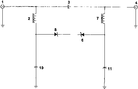
FIG. 1 is a schematic diagram showing a voltage limiter circuit according to
,,
one embodiment of the present invention;
FIG. 2 is a schematic diagram showing a voltage limner circuit according to
another embodiment of the present invention;
FIG. 3 is a schematic diagram showing a voltage limner circuit according to
yet
another embodiment of the present invention; and
FIG. 4 is a schematic view showing the outer surface of a CATV distribution
system device.housing in which a voltage limiter according to the present
invention is
provided.
Detailed Description of the Invention
[0034] The voltage limiter of the present invention operates in connection
with the
particular waveform characteristics of the 60 Hz AC signal provided by the
CATV
power supply. That is, the typical CATV power supply includes a Ferro-resonate
circuit having an output that is substantially a square wave (e.g., quasi-
square wave)
or a sharp transient trapezoidal wave. These types of waveforms offer a higher
level
of efficiency when compared with the standard sine wave AC signal typically
associated with household electrical outlets. Further, the quasi-square or
sharp
CA 02478596 2004-08-19
14
transient trapezoidal waveforms still provide an alternating current that
discourages
galvanic reactions (interactions) between dissimilar metals found within the
distribution line.
[0035] As it is commonly known in the art, the flat tops (as apposed to sharp
or
rounded peaks) of the quasi-square and trapezoidal AC waveform types provide a
longer conduction period (phase) for rectifier circuits within the power
supply systems
for the active device equipment attached to the distribution line. Power
passing
directional taps separate the AC powering voltage signal from the RF
television
signals and pass the power signal through a current limiting, re-settable
fuse. The AC
powering voltage signal is then recombined with the RF signals at the output
ports of
the directional tap.
[0036] As shown in both Figs. 1 and 2, the AC powering voltage signal and RF
signals from a CATV directional tap output, for example, are introduced into
the
voltage limiter of the present invention at an input 1, which can be a stinger
input, for
example, of a sealed CATV filter-type housing. The AC powering voltage signal
and
RF signals are separated by a first RF choke 2 and a capacitor 3, both
positioned
downstream from input 1. The AC powering voltage signal and R.F signals are
separated because the value of capacitor 3 (e.g., 0.0047 microFarad) is chosen
so as to
be a significantly high enough impedance at 60 Hz to'~ffectively block the AC
powering voltage signal while allowing the RF signal to pass with little or no
degradation. The value of RF choke 2 (e.g., 4.7 microHenry) is chosen so as to
be a
significantly high enough impedance at RF frequencies to effectively block the
RF
CA 02478596 2004-08-19
signal while allowing the 60 Hz AC powering voltage signal to pass with little
or no
degradation. Any suitable device could be used to form the RF choke (e.g., an
inductor coil wound around a magnetic core):
[0037] The capacitor 3 is part of a first branch of the overall circuit, and
the first
branch passes from input 1 to an output 4. As such, the capacitor 3 'is
virtually
transparent to the RF signal, such that the RF signal can pass therethrough
without any
significant signal interruption or quality disturbance. The first RF choke 2
is part of a
second, parallel branch of the overall circuit through which the AC powering
voltage
signal passes from input 1 to output 4. The first and second branches are re
joined
upstream of output 4, to allow the RF signals and AC powering voltage signal
to
recombine before exiting the device.
[0038] After the AC powering voltage signal is separated from the RF signals,
it is
passed through a voltage limiting mechanism to lower the amplitude of the
voltage
that exits the device. The Zener diodes 5 and 6 shown in Figs. 1 and ~ achieve
this
objective. While the same two Zener diodes 5 and 6 are included in the
separate
embodiments of Fig. 1 and Fig. 2, the embodiment shown in Fig. 1 differs from
the
embodiment shown in Fig. 2, as will be explained below.
[0039] In the arrangement shown in Fig. l, the two Zener diodes 5 and 6 are
arranged cathode to cathode in series with one another along the second branch
of the
circuit. In this arrangement, both Zener diodes 5 and 6 are in conduction mode
most
of the time, either in normal forward bias mode or in reverse made after the
avalanche
potential has been exceeded.
CA 02478596 2004-08-19
16
[0040] That is, electrical conductivity in a forward bias mode flows through
the
Zener from anode to cathode. Thus, as shown in Fig. 1, Zener diode 5 always
conducts in a forward bias mode (e.g., like a normal diode), but will not
conduct in the
reverse direction until the avalanche voltage of the diode has been exceeded.
Because
of the cathode to cathode arrangement of the Zener diodes, however, Zener
diode 6
will not pass the AC powering signal in the same direction as Zener diode 5
until after
the AC powering voltage signal surpasses the avalanche potential of the Zener
diode
6, that is, after the predetermined (e.g., 30 volts) avalanche voltage is
exceeded.
[0041] Given the alternating directional nature of the waveform of the AC
powering voltage signal, it is necessary to provide two Zener diodes, arranged
cathode
to cathode as shown, to compensate for both the positive and negative regions
of the
AC powering voltage signal waveform. Since each Zener diode must exceed an
avalanche voltage in either the positive region of the AC signal (Zener diode
6) or the
negative region of the AC signal (Zener diode 5) before the entire AC powering
voltage signal can be passed through the second branch of the circuit, the
value of that
avalanche voltage is effectively consumed by the operation of these Zener
diodes.
Consequently, the total voltage of the resultant AC powering voltage signal is
reduced
by the amount of the avalanche voltage in both the positive and negative
regions.
[0042] For example, if it is assumed that the input AC powering voltage signal
is
90 volts RMS and the desired output AC powering voltage signal is 60 volts
RMS, the
Zener diodes 5 and 6 could be selected to have a 30 volt avalanche voltage. If
the
drop line is located a distance from the power supply, however, the actual AC
CA 02478596 2004-08-19
17
powering voltage signal may be something less than 90 volts RMS, for example,
75
volts.RMS due to the aforementioned voltage drops. In this case, when the
desired
output AC voltage remains 60 volts, the Zener diodes 5 and 6 could be selected
to
have a 15 volt avalanche voltage. It should be apparent to those skilled in
the art that
the avalanche voltage of the Zener diodes is not limited to the speczfic
examples
above, and the avalanche voltage of the Zener diodes can be selected to be any
value
depending upon the particular AC voltage at the drop line and the difference
between
the input voltage and the desired autput voltage.
[0043] After 30 volts is stripped from the AC powering voltage signal, it is
passed
through second RF choke 7 and then recombined with the RF signal passing along
the
first branch of the circuit. The second RF choke 7 is necessary to prevent the
RF
signals passing along the first branch of the circuit from entering the second
branch of
the circuit in the same manner that RF choke 2 effectively prohibits the RF
signal
from entering the first branch of the circuit. The value of the second RF
choke 7 is
preferably the same as that of RF choke 2 for the reasons described above.
[0044] Since the Zener diodes shown in Fig. 1 are in conduction mode most of
the
time, heat will be generated when the system is operating at a relatively high
power
level, such as the 5 Watt level required to power residential NIU devices. If
this
excess heat is not effectively dissipated, there is a possibility that the
performance
capacity of the device can be exceeded and failure can occur.
[0045] Implementing steering diodes, such as diodes 8 and 9 shown in Fig. 2,
for
example, reduces the power dissipation requirements of the Zener diodes 5 and
6; and
CA 02478596 2004-08-19
18
improves the performance of the device of the present invention. Fig. 2 shows
a
preferred embodiment of the present invention, wherein two Zener diodes 5 and
6 are
arranged in sub-branches parallel with one another, and wherein each Zener
diode 5
and 6 is further arranged in series, cathode to cathode, with a respective
steering diode
$ and 9.
[0046] The steering diodes 8 and 9 of Fig. 2 essentially allow only one
polarity,
either a positive region or a negative region, of the AC pcawering voltage
signal to pass
to a respective one of the Zener diodes 5 and 6. In this manner, the AC
powering
voltage signal is effectively steered down the two sub-branches such that the
positive
region of the AC signal waveform is reduced by the Zener diode on one sub-
branch
and the negative region of the waveform is reduced by the Zener diode on the
other
sub-branch. Based on the configuration of the diodes shown in Fig. 2, Zener
diode 6
will pass the positive waveform region of the AC powering voltage signal only
after
its avalanche voltage is reached. Similarly, Zener diode 5 will pass the
negative
waveform region of the AC powering voltage signal only after its avalanche
voltage is
reached. The voltage potential of the AC powering voltage signal that is
recombined
with the RF signal after passing through the second RF choke 7 is reduced in
both
regions by the voltage amount that is consumed by each of the Zener diodes as
the
avalanche voltage is reached.
[0047] Since, as described above, the Zener diodes reject reverse current flow
until
the avalanche voltage is achieved, by selecting a Zener diode with a 30 volt
avalanche
voltage, for example, a 90 volt AC powering voltage signal carried at input 1
will be
CA 02478596 2004-08-19
19
reduced to 60 volts AC by the Zener diodes according to the present invention.
The
second RF choke 7 then essentially recombines tlae reduced 60 volt AC powering
voltage signal and the RF signals back together upon the single conductor of
output 4,
which then feeds the drop cable.
[0048] The capacitors 10 and 11 shown in Figs. 1 and 2 form low pass filters
that
prevent any self resonant effects of the RF chokes 2 and 7 from being
transmitted to
the RF signal throughpath along the first branch upon recombination with the
voltage
downstream from the second RF choke 7. That is, while the RF chokes 2 and 7
substantially prevent the RF signals from passing, the possibility remains
that lower
frequency RF signals, such as frequencies less than 5 MHz, for example, might
leak
past the RF chokes and later recombine with the main portion of the I~F
signal. This
can be problematic when the leaked portion of the RF signal is recombined with
the
main portion of the RF signal in an out-of phase state. This type of
disturbance
ultimately affects the overall integrity of the RF signal, degrades the signal
quality,
and reduces the efficiency. Thus, capacitors 10 and 11 are provided to shunt
to
ground any stray portions of the RF signals that manage to leak through the
IZF
chokes, and thus preserve the signal integrity and quality of the RF signal
passing
through the device of the present invention to ensure a seamless IZF
transmission. The
capacitors 10 and 11 each have a capacitance value of about 0.001 microFarads,
for
example, and are therefore a high impedance to tl~e AC powering signal.
[0049] Implementing physically larger Zener diodes also improves the power
dissipation ability of the Zener diodes 5 and 6, and improves the performance
of the
CA 02478596 2004-08-19
device of the present invention. In this case, the sealed housing is required
to be
larger, far example, an Eagle l OM tubular package would be required instead
of a
smaller EM sized package. The increased package size also accommodates
additional
circuitry, such as surge protection devices, self resettable fuses, and
additional
capacitors. An example embodiment of a voltage limiter circuit according to
this
embodiment of the present invention is schematically shown in Fig. 3.
[0050] The voltage limiter shown in Fig. 3 effectively performs the same
function
as those described above in connection with Figs. 1 and 2, and like components
have
been designated with like reference numerals. In addition, however, the
voltage
limiter according to the example embodiment shown in Fig. 3 differs from the
voltage
limiters of Figs. 1 and 2 in the following ways.
[0051] The AC powering voltage signal and RF signals are separated by a first
RF
choke 2 and a capacitor 3, both positioned downstream from input 1. The AC
powering voltage signal and RF signals are separated because the value of
capacitor 3
(e.g., 0.01 microFarad) is chosen so as to be a significantly high enough
impedance at
60 Hz to effectively block the AC powering voltage signal while allowing the
RF
signal to pass with little or no degradation. The value of RF choke 2 (e.g.,
10
microHenry) is chosen so as to be a significantly high enough impedance at RF
frequencies to effectively block the RF signal while allowing the 60 Hz AC
powering
signal to pass with little or no degradation.
[0052] A first surge protection device 12 is provided downstream from input 1
and
upstream from the capacitor 3 on the first branch of the overall circuit,
which passes
CA 02478596 2004-08-19
21
from input 1 to an output 4, as described above in connection with Figs. 1 and
2. The
first surge protection device 12 is also connected to ground as shown. In
addition, a
second surge protection device 13 is provided downstream from the capacitor 3
and
upstream of the output 4 on the first branch of the overall circuit, and is
also
connected to ground, as shown. In that manner, with a pair of surge protection
devices 12 and 13 connected to the RF (first) branch of the circuit and to
ground on
either side of the capacitor 3, the voltage limiter can effectively survive
power surge
waveforms impressed to either input 1 or output 4.
[0053] Any suitable surge protection device can be implemented, and should be
selected based upon the appropriate SCTE standards and desired performance
specifications. For example, as shown in the embodiment of Fig. 3, surge
protection
devices 12 and 13 can be gas tube surge protectors which can suppress up to a
6 kV,
3 kA combination wave surge. This is appropriate for KS port; hard-line style
connectors, for example. The surge protection devices 12 and 13 could also be
spark
gap devices provided in a similar configuration with respect to the voltage
limiting
circuitry. Spark gap surge protectors typically have the ability to suppress
up to 5 kV,
100 A ring wave surges at 100 kHz, which is appropriate for F style
connectors, for
example.
[0054] As described above, after the AC powering voltage signal is separated
from
the RF signals, it is passed through a voltage limiting mechanism to lower the
amplitude of the AC powering voltage signal that exits the device using the
Zener
diodes 5 and 6. In the arrangement shown in Fig. 3, the rivo Zener diodes 5
and 6 are
CA 02478596 2004-08-19
22
arranged cathode to cathode in series with one another along the second branch
of the
circuit, as described above in connection with Fig. 1.
[0055] After the desired voltage value, for example, 30 volts, is stripped
from the
AC powering voltage signal, it is passed through second RF choke 7 and then
recombined with the RF signal passing along the first branch of the circuit.
The value
of the second RF choke 7 is preferably the same as that of RF choke 2 (e.g. 10
microHenry), for the reasons described above.
(0056] The capacitors 10 and 11 shown in Figs. l and 2 form low pass filters
that
prevent any self resonant effects of the R.F chokes 2 and ~ from being
transmitted to
the RF signal throughpath along the first branch upon recombination with the
voltage
downstream from the second RF choke 7, as described above. That is, capacitors
10
and 11 are provided to shunt to ground any stray portions of the RF signals
that
manage to leak through the RF chokes, and thus preserve the signal integrity
and
quality of the RF signal passing through the device of the present invention
to ensure a
seamless RF transmission: The capacitors 10 and 11 each have a capacitance
value of
about 0.001 microFarads, for example, and offer a high impedance to the AC
powering voltage signal. Capacitors 10 and 11 are preferably a disc ceramic,
for
example.
[0057] Another set of capacitors 14 and 15 are also provided to be
electrically
common, but not necessarily physically common, with capacitors 10 and 11,
respectively. In fact, according to a preferred embodiment, the capacitors 14
and 15
are physically located at opposite ends of a signal trace from capacitors 10
and 11.
CA 02478596 2004-08-19
23
The capacitors 14 and 15 are provided for additional filtering and to further
ensure
that the desired output response is flat. Preferably, the value of the
capacitors 14 and
15 differs from that of capacitors 10 and 11 to limit self resonance behavior.
For
example, capacitors 14 and 15 can have a value of 0.01 microFarad. Further,
capacitors 14 and 15 are preferably physically different devices than
capacitors 10 and
I 1. For example, capacitors I4 and 15 can be polypropylene devices rather
than
ceramic discs
[0058] In addition, as mentioned above, the size of the Zener diodes 5 and 6
axe
increased in this embodiment, to better handle the increased power dissipation
requirement as previously discussed. Accordingly, the size of the copper trace
carrying signals between the diodes is also increased correspondingly to
further assist
in the power dissipation. In order to compensate for signal behavior
variations caused
by the increased size of the copper trace, yet another set of capacitors 16
and 17 is
provided between the Zener diodes 5 and 6 to shunt to ground any stray RF
energy
that is coupled from the RF throughpath (first branch) onto the second branch,
which
would otherwise cause undesirable RF throughpath perturbations. That is, the
capacitors 16 and 17 filter any coupled RF energy to ground before that RF
energy
can recombine with the signal on the RF throughpath. The values of the
capacitors 16
and 17 can be, for example, 0.001 microFarad.
[0059] The voltage limiter shown in Fig. 3 also includes a self restettable
fuse 18
between the output of the second branch of the circuit (i.e., the voltage
limiter
mechanism) and the RF choke 7 to prevent Zener diode failure if, for example,
the
CA 02478596 2004-08-19
24
voltage limiter is installed on a drop cable having a "hot" source. For
example,
providing the fuse 18 as shown in Fig. 3 reduces the risk of damaging the
Zener
diodes 5 and 6 if the output of the voltage limner were accidentally shorted
during
installation, for example. The fuse 18 is preferably a polycrystalline thermal
fuse, for
example, that will significantly increase the resistance when a high current
load is
applied and then return to a nominal state once the high current load is
removed.
[0060] It should be apparent to those skilled in the art that the actual
operational
values of the electronic components comprising the present invention, such as
the
capacitance values for the capacitors 3, I0, I I and 24-17, the inductance
values for RF
chokes 2 and 7, and the avalanche values for the Zener diodes 5 and 6, can be
selected
according to the particular characteristics and values of the RF signals and
voltage
waveforms being passed through the device. The values shown herein are used
merely for illustrative purposes, and the present invention is in no way
limited to the
specific examples described herein.
[0061] According to another embodiment of the present invention shown in Fig.
4,
a CATV distribution system device is provided, including a housing 100 having
an
input port 101 configured to communicate with a first coaxial line carrying an
RF
signal and a first AC voltage signal, and an output port I02 configured to
communicate with a second coaxial line carrying the RF signal and a second AC
voltage signal. A voltage limiting mechanism according to any of the above-
described embodiments of the present invention is positioned within the
housing. It
should be noted that, for some embodiments of the present invention, such as
those
CA 02478596 2004-08-19
shown in Figs. 1 and 2, for example, the Eagle l OM type housing 100 shown in
Fig. 4
could be substituted with the Eagle EM type housings described in U.S. Patent
No.
5,662,494, assigned to Eagle Comtronics, Inc., the entirety of which is
incorporated
herein by reference.
[0062) While the present invention has been particularly shown and described
with
reference to the preferred mode as illustrated in the drawings, it will~~be
understood by
one skilled in the art that various changes in detail may be effected therein
without
departing from the spirit and scope of the invention as defined by the
'claims.