Note : Les descriptions sont présentées dans la langue officielle dans laquelle elles ont été soumises.
CA 02482805 2004-10-15
WO 03/090414 PCT/US03/11506
1
2 A Controlled Shared Memory Smart Switch System
3
4
6
7
s Related Patent and Patent Applications
9 The disclosed system and operating method are related
to subject
matter
disclosed
in
the
following
patents
and
patent
applications
that
are
I incorporated
I by
reference
herein
in
their
entirety:
12 1. U.S. Patent No. 5,996,020 entitled, "A Multiple Level
Minimum
13 Logic Network", naming Coke S. Reed as inventor;
I4 2. U.S. Patent NO. 6,289,021entitled, "A Scaleable Low
Latency Switch
I for Usage in an Interconnect Structure", naming John
S Hesse as
16 inventor;
I7 3. United States patent application serial no. 09/693,359
entitled,
I "Multiple Path Wormhole Interconnect", naming John
8 Hesse as
I9 inventor;
4. United States patent application serial no. 09/693,357
entitled,
21 "Scalable Wormhole-Routing Concentrator", naming John
Hesse and
22 Coke Reed as inventors;
23 S. United States patent application serial no. 09/693,603
entitled,
24 "Scaleable Interconnect Structure for Parallel~Computing
and Parallel
2S Memory Access", naming John Hesse and Coke Reed as
inventors;
CA 02482805 2004-10-15
WO 03/090414 PCT/US03/11506
2 6. United States patent application serial no. 09/693,358 entitled,
2 "Scalable Interconnect Structure Utilizing Quality-Of Service
3 Handling", naming Coke Reed and John Hesse as inventors;
4 7. United States patent application serial no. 09/692,073 entitled,
"Scalable Method and Apparatus for Increasing Throughput in
6 Multiple Level Minimum Logic Networks Using a Plurality of
7 Control Lines", naming Coke Reed and John Hesse as inventors; and
8 8. United States patent application serial no. ~lxxx,entitled,
9 "Means and Apparatus for a Scaleable Congestion Free Switching
I O System with Intelligent Control", naming John Hesse anal Coke Reed
I I as inventors.
12 Field of the Invention
13 The present invention relates to a method and means of controlling an
14 interconnect structure applicable to voice and video communication systems
I S and to data/Internet connections. More particularly, the present invention
is
16 directed to a shared memory interconnect switch technology with intelligent
17 control.
Is Background of the Invention
19 A simple data packet switching system found in the prior art consists
20 of a N~~N switch fabric S (often a crossbar) connecting N input ports Io,
II,
21 .. . IN_~ to N output ports Oo, O1, ... ON_1. In a common.configuration,
22 illustrated in Fig. 1, there are buffers IBo, IB1, ... IBN_~ 102 at the
inputs that
23 hold packets waiting to enter the crossbar switch 104. In some
24 configurations, there may also be output buffers OBo, OB1, ... OBN_1 106.
25 Additionally, there is some Iogic (not pictured) to control the crossbar.
2
CA 02482805 2004-10-15
WO 03/090414 PCT/US03/11506
1 In. one simple embodiment, with N input ports, there is a round robin
2 method of controlling the switch. The round robin procedure first permutes
3 the integers 0, l, ... N-1 into a sequence P(0), P(1), ... P(N-1). Then, the
4 logic that sets the NXN switch first examines the data packets at the input
port buffer IB~to~ and selects a packet p~ that it most desires to send
through
6 the switch. If the target output port or target output port buffer is able
to
7 receive a packet, then the logic sets the switch connection to send po to
its
target. If the target output of p~ is not in a condition to receive ~po, then
the
9 logic attempts to send another packet p~ in IBp~p) t0 lts target. This
process is
continued until either: 1) A packet pn in IBP(Q~ is found that can be sent to
its
11 target; or 2) No such packet is found. In case l, one crossbar connection
is
12 set. In case 2, no message from IBr~o) will be sent in the next message
I3 sending period. At this point, the logic sets the switch to send a packet
in
14 IBP~l~ through the switch. For a packet q to be sent from IBP(1~ to it's
target,
it is necessary that the target is in a condition ready to receive a message,
I 6 and moreover, it is necessary that p and q are not sent to the same
output. In
17 general, this process is continued subject to the constraint that no packet
in a
I 8 buffer IBp~K) is sent to an output already scheduled to receive a packet
from
19 IBP~,p, where J < I~. Once the switch is completely set, then the packets
are
sent and the procedure is repeated with a new permutation Q(0), Q(1), ...
21 Q(N-1). The reason for the new permutation is that the early members of the
22 sequence have an advantage over the later members and in order to be fair,
it
23 is necessary that the integers be rearranged for each setting of the
switch.
24 There are a number of disadvantages to the message management
scheme of the prior art: 1) the setting of the switch is, time consuming; 2)
26 the setting of the switch is not optimal; 3) no two output ports can
27 simultaneously receive distinct messages from the same input port. One
3
CA 02482805 2004-10-15
WO 03/090414 PCT/US03/11506
1 example where the setting is not optimal is in the case where a low priority
2 message in IBp(J~ blocks a high priority message in IBP~~), where J < K.
3 While there are numerous variations to shared memory switching systems,
4 the same three problems persist with each of the variations. An example of a
system that overcomes disadvantages 1 and 3 is described in "A Multiple
6 Level Minimum Logic Network" (MLML network) is described in U.S.
7 Patent No. 5,996,020, granted to Coke S. Reed on November 30, 1999,
8 ("Invention #1"), the teachings of which are incorporated herein by
9 reference. Another example of a system overcoming disadvantages 1 and 3
is described in U.S. Patent Application Serial No. 09/009,703 filed by John
11 Hesse on January 20, 1998. ("Invention #2" entitled: "A Scaleable Low
12 Latency Switch for Usage in an Interconnect Structure"). Disadvantage 2 is
13 overcome in the system described in United States patent application serial
14 no. xx/xxx,xxx entitled, "Means and Apparatus for a Scaleable Congestion
Free Switching System with Intelligent Control" (Invention #8). This
16 system uses interconnect structures of the type described in. Inventions #1
17 and #2. A key 'idea in Invention # 8 is to control packet entry into the
data
18 switch by jointly considering all of the messages targeted for a common
19 output port.
It is the purpose of the present invention to use novel new techniques
21 to overcome disadvantages 1, 2, and 3. These techniques use a key idea of
22 Invention #8, of establishing control of the system based on comparing
23 messages targeted for a common output port. However, the present
24 invention does not require the use of self routing networks but rather
relies
on a novel new data management technique. The present invention shows
26 how to manage shared memory switching systems effectively.
4
CA 02482805 2004-10-15
WO 03/090414 PCT/US03/11506
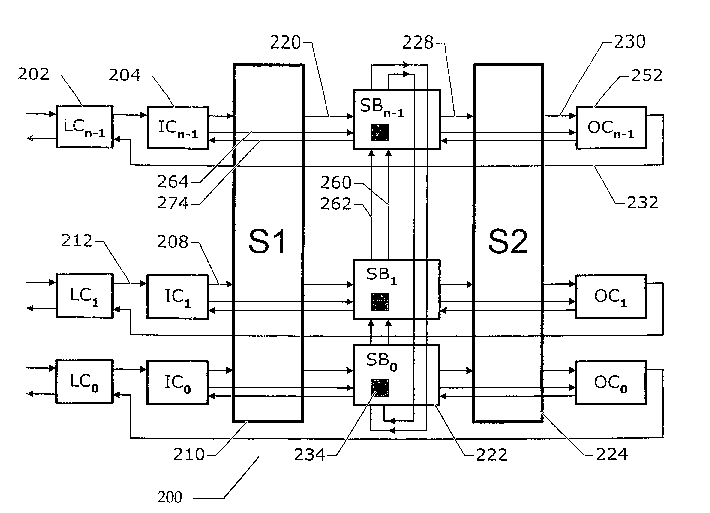
1 Summary of the Invention
2 Refer to Fig. 2 which is a schematic diagram of one embodiment of
3 the present invention. The data entering the system is fed through a first
4 NXN switch S 1 which spreads a single data segment into banks of shared
memory buffers. The data is then sent from these buffers through a second
6 NXN switch S2 that sends the data to the output data buffers. It will be
7 shown later in this patent that the spreading out of the data in a certain
way
8 makes it possible to have a good strategy for choosing which messages to
9 send through the switch S2. Moreover, the switches S 1 and S2 switch in a
systematic fashion governed by a clock so that there is no time consuming
I I data dependent method of setting the switches S1 and S2.
12 In the following discussion, sequences of N items, such as controllers
13 or buffers, will be used. These items will be labeled using the integers 0,
1,
14 2, ... N-l, so that one of these sequences would be denoted by Xo, Xl, X~,
...
1 S XN_1. At times it will be convenient to tally about XJ~.K Or XT_~, where
each of
16 J and K is an integer in the range 0 to N-1. Since "J+K" and "J-K" must
17 also lie in the range 0 to N-1, modulo N (mod N) arithmetic will be used.
18 Thus, when "J+K" or "J-K" is used as a subscript, it will be understood
that
19 "J+K" is shorthand fox (J+K+N)mod N and "J-K" is shorthand for
(J-K+N)mod N. For example, if N=8, J=5 and K--7, then (J+K+N)mod N =
21 (5+7+8)mod 8 = 4 and (J-K+N)mod N = (5-7+8)mod 8 = 6.
22 Each of the N inputs feeds into a line card 202 that prepares the data
23 for entry into the switching system. The line card sends the data through
24 data lines 212 to the input controllers ICo, ICI, ..., ICN_~ 204. The input
controllers break the packets into segments of length SL bits and then further
26 break the segments into N sub-segments (flits) each of length FL bits. FL
5
CA 02482805 2004-10-15
WO 03/090414 PCT/US03/11506
1 and SL are chosen so that SL=NFL and these two values are optimized with
2 respect to the size of the switching system and the size of the packets that
it
3 handles. The input controllers contain logic and memory buffers (not shown
4 in FIG. 2). The input controllers perform a number of functions. They send
the flits through lines 208 to S1 210. Data passes from S1 through lines 220
6 to the shared buffers SBo, SB1, ... SBN_1222. A given input controller
stores
7 data in all of the shared buffers. In fact, each segment is composed of N
flits
8 (denoted by Fo, Fl, .. . FN_1) and for a given message segment, an input
9 controller places one flit in each of the shared buffers. Fig. 2 shows grey
areas 234 where the flits of a message segment are stored in the same
11 relative location in each of the shared buffers. Data passes from the
shared
12 buffers to switch S2 224 through Lines 228. Data then proceeds from S2 to
13 the output controllers 252 through Lines 230. Finally, data passes from the
14 output controllers to the line cards 202 through the interconnect lines
232.
The switches S1 and S2 operate in a systematic manner. In this
I6 simplest embodiment, it is assumed that S 1 and S2 are crossbar switches.
17 Data can move bit serially or in wider paths. In the simple embodiment
18 described here, data moves bit serially. A time unit T is defined as the
19 number of clock ticks that it takes to set the switch S 1 and then to move
a flit
consisting of FL bits from an input controller to a shared buffer through line
21 208, switch S1 and line 220. The system is designed so that it also takes T
22 clock ticks to set the switch S2 and then to move a flit from a shared
buffer
23 to an output data buffer through Line 228, switch S2 and Line 230. A
24 message segment cycle is composed of N time intervals, each of length T,
and will be identified by [0, T], [T, 2~T], ... [(N-1)~T, N~T]. Negative
26 coefficients for T, such as [-T, 0], will be used to denote time intervals
in the
27 cycle previous to the one being discussed. Suppose that a message segment
6
CA 02482805 2004-10-15
WO 03/090414 PCT/US03/11506
I M is at input controller ICS, then during time interval [0, T], S 1 is at a
2 setting so that the input controller ICS sends the first flit of data
through the
3 switch S 1 to the Kth shared buffer SBK. During time interval [T, 2~TJ, S 1
is
4 at a setting so that ICx sends the second flit of data through S 1 to shared
buffer SBA+1. This process continues through time interval [(N-I)~T, N~T],
6 in which ICS sends the Nth and last flit of the message segment M to shared
7 buffer SBK+~_1>. At the end of this message segment cycle, each of the
8 shared buffers contains FL bits (one flit) of the message segment M.
9 The movement of the data from one location to another is summarized
I O in the Table I timing chart. This timing chart also shows the movement of
I 1 certain control signals including those control signals discussed in the
next
12 paragraph. The timing chart of Table 1 summarizes data and control signal
I3 movement described in a number of sections of this patent.
14 In addition to sending the message segment M to the shared buffers,
I S the input controller ICK also sends control information. Whereas ICre
sends
I6 data bits in each of the time intervals [0, T], [T, 2~T],... [(N-1)~T,
N~T], the
I 7 input controller ICI{ sends a control information paclcet (CIP) to SBI~
only in
18 the time interval [-T, 0] (which is used to denote the last interval,
I9 [(N-1)~T, N~T], of the previous cycle). The packet CIP passes from ICr~ to
20 SBK through line 264. This control information packet contains information
21 concerning the message segment M including: 1) the relative memory
22 location of the flits of M in the shared buffers; 2) the target output of
M;
23 3) the priority of M; 4) a unique message identifier; and 5) an end of
24 message flag. The control information is located in a special reserved
25 location in memory buffer SBK.
26 The input controllers direct the writing of data to the shared buffers:
27 The output controllers direct the reading of data from the shared buffers.
7
CA 02482805 2004-10-15
WO 03/090414 PCT/US03/11506
1 Both the input controllers and the output controllers send control
2 information to and receive control information from the shared buffers. The
3 amount of time N~T that it takes to write a complete message segment to the
4 shared buffers is referred to as a cycle time or as a segment insertion
cycle
time or simply as a cycle. A message segment writing period is referred to
6 as a cycle period. A message segment writing period is divided into the N
7 tune intervals [0, T], (T, Z~T], ... [(N-1)~T, N~T].
A set of lines used for passing control information from an input
9 controller to an output controller or from an output controller to an input
controller will be referred to as a "control path" and consists of the
11 following: 1) a set of lines connecting each input controller to its
12 corresponding shared buffer, 2) a set of lines for communicating within.
the
13 shared buffer system, and 3) a set of lines connecting each output
controller
14 to its corresponding shared buffer. Importantly, note that a control path
does
not pass through either of the switches S 1 or S2. Two control paths are
16 present in FIG. 2: a control path consisting of lines 264, lines 260 and
lines
17 270 that allow an input controller ICS to send control information to an
18 output controller OCJ, and a control path consisting of lines 26f, lines
262
19 and lines 274 that allow an output controller OCJ to send control
information
to an input controller TC~. A packet P originating in input controller TCL or
21 in output controller OCL will be said to "propagate" or "percolate" through
22 the shared buffer system if there is a sequence of consecutive time
intervals
23 Io, h, . . . IN_1 such that P is in SBL+M at the beginning of time interval
IM,
24 where M is an integer in the range 0 to N-1. Note that each input
controller
ICM or output controller OCM is in position to read packet P during time
26 lnterVal IM_L SlnCe P is in SBM at the be,~ning of this interval. All
control
27 information percolates through the shared buffer system.
CA 02482805 2004-10-15
WO 03/090414 PCT/US03/11506
1 During the time interval [-T, 0], input controller ICS sends a control
2 information packet CIP associated with message segment M through line
3 264 into SBx. During the time interval [0, T], this control information
4 packet is sent from SBK to SBA+1 and also from SBK to OCK. During the
time interval jT, 2~T], this same control information packet is sent from
6 SBA+1 to SBA+2 and also from SBA+1 to OCK+1. This process continues
7 throughout the cycle so that at the end of the cycle, each output controller
8 has read the control information packet associated with message M. A
9 control information packet travels from a shared buffer to an output
controller through line 270. When an output controller OCJ reads a control
11 information packet for a message segment packet targeted for output port J,
12 the output controller stores this information in its output control buffer
13 OCBJ. In the present embodiment, output controller OCJ discards
14 information concerning messages targeted for output ports distinct from J.
In this manner, each output controller OCJ is able to keep track of the
16 location and priority of all messages targeted for output port J. An output
17 controller OCJ is able to tell which input port a given segment entered
based
18 on the time interval in which it extracts the control information packet
CIP
19 for that segment from the shared buffer SBJ. Thus, for example, OCJ
calculates that the CIP read from SBJ in the third time interval [2~T, 3~T]
was
21 originally loaded into SBJ-2 by ICJ-2 in time interval j-T, 0]; i.e. K=J-2.
22 Hence, the control information packet CIP advantageously need not include
23 input port information.
24 The output controller OCJ examines a CIP for each segment inserted
into the shared buffers. If there is a message segment in the shared buffers
26 targeted for output port J and OCJ has examined its CIP, then at a time
27 interval [0, T], OCJ begins to transfer one of these message segments to
its
9
CA 02482805 2004-10-15
WO 03/090414 PCT/US03/11506
1 output data buffer ODBJ. The output controller is able to make a reasonable
2 decision as to which message to read, choosing lv.gher priority messages
3 over lower priority messages. During time [0, T], OCJ directs a flit FP of a
4 message sent by ICK from shared buffer SBJ to its output data buffer ODBJ
650. Notice that ICK places flit Fp in shared buffer SBK+P and therefore, J =
6 K+P and P = J-K. But output controller OCJ can calculate the value of K
7 because OCJ previously read the control packet inserted in SBK by ICK.
8 Therefore OCJ can calculate the value of P. Thus the packet segment is read
9 out in the order FP, FP+1, . . . , FN-1, Fo, Fi, . .. , FP-I. It is one of
the tasks of
the output controller OCJ to place the flits of the segment in the proper
order.
11 In time interval [-T, 0], OCJ sends a special memory location available
12 . packet MLA through line 266 to SBJ indicating that the address specified
in
I3 MLA will be available at the end of the current segment reading cycle. The
I4 information in MLA is a complete description of the physical location of a
flit in a shared buffer, giving both its input port number and its relative .
1 b storage address SA. For example, port number K and relative address SA
17 would indicate that the flits of a segment were placed in the set of shared
1 S buffers at relative address SA within the set of flit memory banks MK. At
19 time interval [(K-J)~T, (K-J+1)~T], ICx reads this MLA packet from SBK
indicating that address SA will be available for another message (MLA is
2I moved from buffer to buffer in the shared buffer system in a manner similar
22 to CIP as described above). If the port specified is K, then ICK adds the
23 location SA to its list of free memory locations; otherwise, ICK ignores
24 MLA.
The input controllers are responsible for discarding message packets
26 when an overflow condition is imminent. Such conditions could arise if
27 more than one input controller sends multiple high priority message packets
CA 02482805 2004-10-15
WO 03/090414 PCT/US03/11506
1 to an output port J, while ICK also sends multiple lower priority message
2 packets to J. Various schemes of handling overflow conditions are possible.
3 Further discussion of this topic will be included in the section on the
input
4 controller.
The present invention has a novel scheme of directing message sub-
6 segments into the correct physical data storage locations within the shared
7 buffer. The storage address is sent by a separate channel and arnves before
8 the message so that the switches internal to the shared buffer that direct
data
9 from S I into the proper storage location axe set just in time for the
arrival of
the message. Similarly, the address of the sub-segment to be output from the
11 shared buffer into the switch S2 arrives just in time to direct the proper
data
12 sub-segment into S2. Neither header information nor control information
13 pass through S I or S2, whereas alI of the data passes through both
switches.
14 The separate movement of the addresses and control information in the
shared buffer is important and advantageous since each segment is
16 decomposed into N sub-segments (flits) and placing the identical header in
17 front of each of the messages would be time consuming.
is Brief Description of the Drawings
19 FIG. 1 is a schematic block diagram showing an example of a generic
prior art switching system consisting of line cards, shared buffers, a switch
21 fabric, and output buffers.
22 FIG. 2 is a schematic block diagram illustrating the intelligent shared
23 memory switching system of the present invention. The system includes
24 Line cards, input controllers, an input switch S1, shared buffers, an
output
switch S2, and output controllers.
11
CA 02482805 2004-10-15
WO 03/090414 PCT/US03/11506
1 FIG. 3 is a schematic block diagram illustrating an input controller
2 used in the present invention.
3 . FIGS. 4A through 4G are diagrams showing formats of packets used
4 in various components of the switching system.
FIG 5 is a schematic block diagram of a shared buffer of the present
6 invention.
7 FIG.6 is a schematic block diagram of an output controller used in the
8 present invention.
9 FIG. 7 is an illustration of the shift register that carries the CIP
packet.
11 FIG. 8 is an illustration of a Banyan switch that is a suitable design
12 for use as S 1 or S2.
13 FIG. 9 is an illustration of a switch A with multiple output lines to
14 switches Bo, B1, ... ,BP, ... , BM_l.
1 s Detailed Description
16 In order to understand the operation of the system 200, it is necessary
17 to have in depth knowledge of the operation of the input controllers,
output
18 controllers, shared buffers, and switches S 1 and S2. It is also necessary
to
19 understand the content and format of the data carrying packets as well as
the
content and format of control information carrying packets.
21 Description of Packet Formats and Layouts
22 The data packets entering the system are decomposed into segments
23 and further decomposed into flits. These flits move through system and are
24 reassembled into segments, which in turn are reassembled into output
message packets. The flits are directed from input ports to output ports
12
CA 02482805 2004-10-15
WO 03/090414 PCT/US03/11506
1 through the switches S 1 and S2. In addition to the message packets, there
2 are a number of control information packets that are sent from location to
3 location in the system. The control information packets do not travel
4 through the switches S 1 and S2. Prior to describing the components
illustrated in system 200, the formats of the data carrying packets and
6 control packets will be described.
7 FIG. 4A shows the format of a message packet as it is received by a
8 line card and passed on to an input controller. A message packet consists of
9 a header and a payload. FIG. 4A also shows how this message is
decomposed into segments and flits. The message length determines the
1 I number L of associated segments. The message packet 400 is decomposed
I2 into segments So, S1, S2, ... SL_1. Each segment SX in the segment sequence
I3 is further decomposed into N flits Fo, F1, ... FN_1. Each flit contains FL
bits
14 and each segment contains SL bits, where SL = NFL.
I 5 FIGs. 4B to 4G show the structure of the various control packets
16 referred to in this document. Following is a brief description of the
fields
17 within these control packets:
18 BIT - A one bit field set to one to indicate the presence of a packet.
19 changing BIT to zero will "erase" the packet.
MTA - The message target address, i.e. the destination output port of an
21 incoming message packet. The MTA is derived from information in the
22 incoming message packet header.
23 SA - The relative segment address for a set of flits in the shared buffer
24 system.
SP - The segment priority, which is based on the quality of service (QOS)
26 value in the header of the incoming message.
I3
CA 02482805 2004-10-15
WO 03/090414 PCT/US03/11506
1 MPIL~ - The message packet 1D selected by the input controller to identify
2 each segment of a given message packet.
3 EOM - An end of message indicator. A one bit field included in several
4 control packets to indicate that a complete message packet has been
processed. EOM is set to zero, unless the control packet is associated with
6 the last segment for a message packet, in which case it is set to one.
7 IP - The number of the input port that sent the segment associated with the
8 control packet.
9 OP - The number of the output port sending the control packet.
NUMX - The number of segments having priority X.
11 Component and Timing Description
12 In order to have a complete understanding of the invention, it is
13 necessary to have an in depth comprehension of: 1) the operation of the
14 switches S l and S2; 2) the operation of the input controllers; 3) the
operation
of the output controllers; 4) the construction and operation of the shared
16 buffers; and 5) the timing of the system. Each of these topics will be
17 discussed in a separate section. The input controllers and output
controllers
18 have functions that are similar to those of the input controllers and
output
I9 controllers in patent 8. These interconnect controllers provided by the
present invention and patent 8 make possible a level of intelligence not
21 found elsewhere. This control is accomplished by simultaneously
22 examining all of the messages targeted to a given output port and by using
23 this information to route the data. The shared buffers constitute the novel
24 shared memory and logic that are at the heart of the patent. A key aspect
of
the invention is the novel timing scheme. There is a global clock that drives
26 the system. Message packets are decomposed into segments and segments
14
CA 02482805 2004-10-15
WO 03/090414 PCT/US03/11506
I are fixrther decomposed into sub-segments referred to as flits. A flit
consists
2 of FL bits, and a segment consists of SL bits, where SL = NFL. It requires
3 T clock ticks to move a flit from one location to another. A global clock GC
4 (not illustrated) initializes time to zero. This clocks steps sequentially
to
time N~T (the amount of time required to move a segment) then resets to
6 zero. In this document, when it is stated that a certain event occurs at
time t,
7 it is implied that t is the setting of the global clock when the event
occurs.
The Switches S1 and S2
9 A novel and important feature of the present invention is the presence
of the data switches that are reset by a central clock rather than by a
strategy
11 that is data dependent. In the time interval [0, T], the switches S l and
S2 are
12 set so that, during that time period, data traveling through S 1 travels
from
I3 ICK to SBK and data traveling through S2 travels from SBK to ODB~. In the
14 time interval [T, 2~T] data travels through S1 from ICK to SBK+i and data
travels through S2 from SBA+I to ODBK. This switching pattern continues
I6 so that in the time interval [M~T, (M+1)~T] data travels through S1 from
ICS
17 to SBA+M and through S2 from SBK+M to ODBK.
is Input Controllers
19 FIG. 2 depicts a switching system 200 with intelligent control. A
message packet enters a line card LCK 202. The message packet can be one
21 of a variety of formats including Ethernet, Internet Protocol, Sonnet
Frame,
22 and ATM. The line card LCK sends a message packet MP in the form of
23 FIG. 4A to input controller ICS. The packet MP consists of a header and a
24 payload. The header contains information including the final destination of
the message packet from which the message target address (MTA) is
CA 02482805 2004-10-15
WO 03/090414 PCT/US03/11506
1 derived. This header also contains quality of service (QOS) information
2 from which the segment priority SP is derived. FIG. 3 depicts the
3 components of an input controller 204 consisting of an input controller
logic
4 ICL 310, an input data buffer IDB 320, a list of available shared buffer
storage locations ASL 330, and a list of available message packet IDs ANNlm
6 340. The input controller ICK receives messages from a line card through
7 interconnection line 212 and sends message flits to S I through Iine 208.
The
8 input controller sends control information packets to SBA through line 264
9 and receives storage location available information from SBA thorough line
274. In response to the arrival of a message MP from the line card, the input
11 controller ICK performs a number of tasks including the following:
12 ~ The data in the message packet MP arriving at ICS (including the
13 . packet header information) is decomposed into message packet
14 segments as illustrated in FIG. 4A. The segments are all of the same
length SL. The number of segments depends upon the length of MP.
16 The segments consist entirely of incoming data and do not have
17 header information inserted by the switch system 200. Instead,
18 required information needed to route messages through system 200 is
19 placed in a separate control information packet CIP, as illustrated in
FIG.4B.
21 ~ A segment S is decomposed into N sub-segments (flits) Fa, Fi, .. . FN_z
22 each of length FL as illustrated in FIG. 4A.
23 ~ A segment address SA is chosen as a shared buffer storage location
24 for the segment S. This address is taken from the list of available
shared buffer memory locations stored in ASL.
26 ~ A priority SP for the segment S is chosen. This priority value is based
27 at least in part on the quality of service of the packet MP. The priority
16
CA 02482805 2004-10-15
WO 03/090414 PCT/US03/11506
1 value may also depend upon other factors, including the other data in
2 the shared buffers.
3 ~ A unique message packet identifier MPID is chosen for the message
4 MP from the AMm buffer. This message identifier is used by the
output controllers in re-assembling the segments into a message
6 packet.
7 ~ The last field of each CIP is the end of message indicator EOM. This
8 is a one bit field whose value is set to one to indicate that a given
9 segment is the last segment .of the packet and is set to zero otherwise.
This bit alerts the output controller that the unique message packet
11 identifier MPID is free to be reused for another packet.
12 ~ A control information packet CIP containing the fields MTA, SA, SP,
13 MPG, and EOM is constructed. The CIP packet is illustrated in FIG.
14 4B.
~ In the time interval [0, T], the flit Fo of S is sent from ICK to SBA
16 through line 208, switch S l and line 220 and is stored in shared buffer
17 SBK at segment address SA in flit memory bank M~. In the time
18 interval [T, 2T] the flit Fl of S is sent through line 208, switch S 1 and
19 line 220 for storage in SBK+i at address SA of MK. This process
continues until in the time interval [(N-1)~T, N~T] the flit FN_1 of S is
21 sent to SBg+N-1 for storage at address SA in M~. The shared buffer
22 subscripts are non-negative integers less than N because the addition
23 is done mod N.
24 ~ In time interval [-T, O], CIP is sent on Line 264 to location CM1 530 of
SBA as illustrated in FIG. 5.
17
CA 02482805 2004-10-15
WO 03/090414 PCT/US03/11506
I ~ In each time interval [QT, (Q+I)~T], ICK examines a special location
2 CM2 532 of SBK for an MLA packet. MLA contains an input port IP
3 number, a segment address SA and an end of message flag EOM. If
4 an MLA packet is present in CM2 (i.e. BIT = 1) and IP is K, then the
value of SA is in MK. If such a value is present, then ICK adds the
6 value of SA to its ASL and "erases" MLA by changing the first bit
7 (BIT) to zero. In addition, if IP is K, ICK also checks to see if the
8 EOM field is one. If so, ICx alters the AMID buffer to allow the reuse
9 of MPID for another message packet. If no SA value is present or the
value is in a buffer ML with L distinct from K, then ICS does not
I 1 modify its ASL nor does it modify CM2.
12 ~ In time interval [-T, 0], ICS sends SA (as a subfield of CIP) on line
13 264 to SBK to be used by the logic of SBK in the time interval [0, T] to
14 route Fo to its proper storage location. [-T, 0] is used to denote the
last time interval in the previous cycle. Thus, in the T ticks
16 immediately prior to sending Fa to SBK, the controller ICK sets up the
17 storage location for Fo.
18 ~ In any switching system a data overflow situation may occur, forcing
19 message packets to be discarded. In a simple embodiment of this
invention, two methods of selecting message packets for discarding
21 may be employed: 1) A number MAX can be set such that each input
22 controller and each output controller will discard any message
23 segments that remains in the system longer than MAX cycles. And
24 2) If an input controller ICK receives a message packet from its line
card and its input data buffer IDB~ is nearly full, then ICS compares
26 the priority of the incoming message packet with the set of
27 unprocessed entries in IDBK with Iowest priority. ICS then discards
18
CA 02482805 2004-10-15
WO 03/090414 PCT/US03/11506
1 the packet having the lowest priority, either the incoming packet or
2 one in its input data buffer. Note that an unprocessed entry is one that
3 has been received by the input controller but has not yet had any of its
4 segments sent to the shared buffer system.
~ In a first additional control embodiment; if an overflow condition
6 arises at input controller ICS due to congestion at output port J, ICS
7 can relieve this situation by increasing the priority of its message
8 packets targeted for J. To do this, ICK creates a change priority packet
9 CPK (illustrated in FIG. 4F) which specifies a message target address
MTA of J, the message packet ID MPID of the packet to be changed,
11 and the new priority SP for the packet. ICK updates the priority for
12 any segments of the packet not yet sent and sends CPK via a control
I3 path (not shown) to the output controllers. CPS percolates through the
14 shared buffer system using location CM3. In embodiments using
change priority packets, there are additional lines from ICS to SBA,
16 from SBA to OCJ and between shared buffers. Each output controller
17 will examine CPS, and OCJ will note that CPK is directed to port J,
1 S while the other output controllers will ignore the packet. OCJ will
19 then change the priority for all of the segments of the spec'>fled
message packet in its output controller buffer.
21 ~ In a second additional control embodiment, an input controller ICK
22 may also discard a partially processed message packet in order to
23 avoid overflow. To do this, ICS sends a discard message packet DMK
24 (see FIG. 4E) to the appropriate output controller via a control path
(not shown) and discards whatever segments of this packet remain in
26 IDBK. The DMA packet percolates through the shared buffer system
27 using location CM4. In embodiments using discard message packets,
19
CA 02482805 2004-10-15
WO 03/090414 PCT/US03/11506
1 there are additional lines from ICS to SBA, from SBJ to OCJ and
2 between shared buffers. Each output controller OCJ Will read the
3 DMA packet and ignore it if MTA is not J. If MTA is J, OCJ will
4 delete all segments associated with input port K and the MPID
supplied, thus completing the deletion of the requested message
6 packet.
7 ~ Additionally, there may be error detection and possible error
8 correction functions performed by the input controller.
9 ~ Also, the input controller can send information through its
corresponding line card (or in a separate line that does not pass
11 through the line card) to the output port of an upstream device. This
12 information indicates the status of the input port. The upstream
13 devices could use this information to regulate the flow of data to the
14 switch 200. The path of the control information between separate
switches is not indicated in FIG. 2. This information can fan out
16 upstream through the entire system.
1~ Output Controllers
18 FIG. 6 illustrates the main components of an output controller. The
19 output controller contains a logic unit OCL 610, an output data buffer ODB
650 and output control buffer OCB 620 that holds the output contxol packets
21 (OCP). The OCP packets are built using information in the CIP packets.
22 The logic unit takes the information in the OCP packets as input, and based
23 on this information, it manages the flow of traffic from the shared buffers
24 222 to the output data buffers 650 and from the output data buffers to the
line cards 202. Line 270 delivers CIP packets, and line 266 sends an MLA
26 packet to notify an input controller that a memory location in the shared
CA 02482805 2004-10-15
WO 03/090414 PCT/US03/11506
1 buffers is free. As in patent 8, an output controller is associated with a
given
2 output port (including, in this case, an output data buffer and a line
card).
3 The output controller examines all of the traffic that is targeted to its
4 associated output port and controls the flow of data into the line card
associated with that output port. The routing of messages based on the
6 comparison of two or more messages at different input ports targeted for the
7 same output port is a key feature of the present invention as well as patent
8.
8 In order for this to be possible, it is necessary that the output controller
OCJ
9 be informed of all of the traffic targeted for output port J. The
information
needed by the output controllers is contained in the control information
11 packet CIP. In case a message packet MP targeted for line card LCJ arrives
12 from outside the system at Line card LCD, the input controller ICx segments
13 the message and, corresponding to each message segment M, the input
14 controller ICS constructs a control information packet CIP. During the last
time interval of each cycle, ICx places CIP into the CMl section of SBA. In
16 this manner, the input controller ICx writes to location CM1 of SBA in each
17 cycle time interval of the form [(N-1)~T, N~T] (often referred to as [-T,
0] to
18 emphasize that an event occurs in the last time interval of the cycle
before its
19 use). The output controller makes decisions based on the information that
the input controllers place in the CMl sections of the shared buffers.
21 The output controller OCJ performs a number of functions including
22 the following:
23 ~ During the time interval [T, 2~T] the output controller OCJ reads the
24 control information packet CIP (inserted by input controller ICJ_1)
from location CM1 of SBJ. During the time interval [2~T, 3~T], the
26 output controller OCJ reads the CIP packet (inserted by input
27 controller ICJ_Z) from SBJ. This process continues so that in time
21
CA 02482805 2004-10-15
WO 03/090414 PCT/US03/11506
1 interval [(N-1)~T, N~T] the output controller OCJ reads the CIP packet,
2 which was inserted by ICJ~_l~, from location CM1 of SBJ. Note that
3 SBJ_~_1) 1S SBJ+1.
4 ~ Each time OCr reads a control information packet CIP and the MTA
field of CIP is J, OCJ places information from CIP in an output control
6 packet OCP of the type illustrated in FIG. 4E. The output controller
7 then stores this OCP packet in the buffer OCB 620, and "erases" the
CIP packet by changing the first bit (the traffic bit) to zero. In the
9 simplest embodiment, OCJ ignores control information packets whose
message target address field is not J.
11 ~ If at time (N-3)~T there are any control information packets in the
12 OCB buffer of OCJ, then in the time interval [(N-2)~T, (N-1)~T], the
13 output controller OCJ chooses one of the OCP packets OCP* and
14 initiates a sequence of events associated with packet OCP'~. As a
consequence of the choice of OCP*, the segment associated with
16 OCP* will be transferred from the shared buffers to ODBJ. In the
17 simplest strategy, OCP* is associated with a segment of highest
18 priority to be sent to ODBJ. The output controller causes the segments
19 of a given message to be sent in order. In case there are two messages
with the same highest priority, the output controller can base its
21 choice on the time the segments entered the shared buffer.
22 ~ In the time interval [(N-1)~T, N~T], OCJ creates an MLA packet,
23 which contains the SA field of OCP*, and sends it through line 266 to
24 the CM2 field of SBJ. Notice that because of the use of modular
arithmetic, [(N-1)~T, N~T] = [-T, 0]. One purpose of this action is to
26 cause the segment in location SA to be sent to ODBJ during the next
22
CA 02482805 2004-10-15
WO 03/090414 PCT/US03/11506
1 cycle. Recall that during this same time interval, ICJ creates a CIP,
2 which contains an SA field, and sends it to the CMl field of SBJ.
3 ~ In the time interval [-T, 0], OCJ sends the values of K and SA in an
4 MLA packet (illustrated in FIG. 4F) to the CM2 field of SBJ, where K
is the subscript of input controller whose message is being processed.
6 The purpose of this action is to allow ICK to free up this space in its
7 ASL for another message segment.
8 ~ In some embodiments of this invention, an output controller OCJ
9 sends status information to all of the input controllers. There are four
types of status information that OCJ can send to the input controllers.
11 The information is sent in an output port status packet OPSJ (see FIG.
12 4G). The first type of information is a sequence of numbers NCTMo,
13 NUMI, ... NUML, where NLJM~ gives the number of message
14 segments in OCBJ having priority X. The second type of information
that the output controller can send may contain information (not
16 illustrated in FIG. 4G) about the number of message segments of
17 various priorities in the shared buffer that are targeted for OCJ. The
18 second type of information can be included in the OPSJ packet or sent
19 in a separate control packet. A third type of information that an
output controller can send is information that it has received from a
21 down stream input port or downstream input port controller (usually
22 one that receives data from the output port associated with OCJ). The
23 third type of information can include the status of the downstream
24 buffer or any other information that is useful to the network system
management. This third type of information can be sent with the
26 information of type one or type two or can be send in a separate
27 packet. A fourth type of information that an output controller can
23
CA 02482805 2004-10-15
WO 03/090414 PCT/US03/11506
1 send lists the number and priority of messages recently received by
2 the output port. As before this information can be sent in a control
3 packet with information of type one, two or three or it can be sent in a
4 separate control packet. The fourth type of information indicates a
likely busy condition of a down stream input port and is useful when
6 the downstream input port does not send status information back to
7 OCJ, or else it does not send this information back in a timely manner.
8 An input controller can use this information to tell how busy each
9 output port is and use this knowledge in selecting which segments to
send. An output port status packet OPSJ is sent via a control path (not
11 shown) in the same manner as an MLA packet. Other possible control
I2 packets for information of type two, three, or four may require
13 additional buffer locations and control lines, also not shown. OPSJ
14 and other possible output port status packets percolate through the
I 5 shared buffer system using storage buffer locations CMS and
I6 additional lines not shown. Thus each input controller will have an
17 opportunity to read OPSJ or other output port packets within N time
18 intervals.
I 9 ~ In an alternate embodiment, the output controller has the ability to
discard packet segments in its buffer. In this case, the output
21 controller generates an additional control packet to inform the input
22 controllers of this action.
~3 The information that the output controllers send back to the input
24 controllers allow the input controllers to apply a level of control not
possible
without this information. In particular, information of type three from a
26 downstream input port of a separate device can itself be based on
27 information received from yet another separate device still further
24
CA 02482805 2004-10-15
WO 03/090414 PCT/US03/11506
1 downstream. In this manner, information can travel upstream from switch to
2 switch. This information can fan out upstream and can be used to give a
3 new and novel level of control to the entire system.
Shared Buffers
The line cards send data packets to the input controllers. The input
6 controllers send data through the switch Sl to the shared buffers. The
7 shared buffers send data through S2 to the output data buffers. FIG. 5 is a
8 detailed block diagram of a shared buffer 222. A system with N input ports
9 has N shared buffers. Each of the N shared buffers contains a number of
components including N flit memory banks M~, Mi, . . . MN 1510; two
11 control information storage areas CMl 530 and CM2 532; and a logic unit
12 SBL 520. Memory bank' M~ is reserved for data that entered the system
13 through input port I~. Data in M~ can be targeted for any output port. Trl
14 some embodiments, the N memory banks are of equal size. In other
embodiments, there is a memory manager that allocates different amounts of
16 memory to different input ports. This feature is usefizl when some input
17 ports are not connected to data lines or when different data lines receive
data
18 at unequal data rates. Associated with each flit memory bank MK, there
19 corresponds a list of addresses in M~ that are not in use and are therefore
available to store new data. This list of available addresses is stored in the
21 ASL 330 memory unit in input controller ICS. The storage location CMl
22 530 holds a single CIP packet that is inserted by the single input
controller
23 ICS and is read by all of the output controllers. The storage location CM2
24 532 holds a single free memory packet MLA indicating a free memory
position in one of the flit memory banks in the sequence Mo, Ml, . .. MN_i
26 510. CM2 receives its single data item from an output controller OCJ that
CA 02482805 2004-10-15
WO 03/090414 PCT/US03/11506
1 reads a data item originating from input controller ICK. When OCJ reads an
2 item from location MP of MK, then OCJ indicates that position MP is free to
3 hold new data by inserting the address MP into CM2. CM2 is read by all of
4 the input controllers and is used by a single input controller ICS. The
shared
buffer SBA is governed by a logic SBL S20 that receives control input from
6 SBA 1 through lines 260 and 262 and sends control output to SBA+1 through
7 Lines 260 and 262. This logic unit controls the storage of data into SBK
8 through line 220 and also controls the sending of data out line 228. The
9 logic unit SBL 520 controls the flow of a segment from the switch S 1 into
the correct location SAI in the shared buffer data storage area. Logic unit
11 SBL also controls the flow of data from the correct memory location SAO in
12 the shared buffer to the output data buffers. These correct memory
locations
13 are passed to the shared buffer as SA packets.
14 The timing of the data and the control information is critical to the
correct operation of the shared buffers. A flit of data arriving at a shared
I6 buffer SBL through line 220 is stored at a location that is determined by
the
17 SA field of a MLA packet that arrives on line 260. During the time interval
18 [-T, 0] an input controller ICK scheduling flit Fo arnval beginning at the
next
19 time 0 (the beginn?ng of a segment sending cycle), sends a CIP packet
containing segment address SA to SBA through line 264. This CIP packet is
21 stored in location CM1. At time 0, the shared buffer internal memory switch
22 is positioned to place the next arriving data (the flit Fo arriving in time
23 interval [0, T]) in memory location SA in. memory bank MK of SBK. During
24 the time interval [0, T] while Fo is arriving at storage location SA in
memory
bank MK, SBK sends SA to SBA+1 through line 260. This address is in place
26 when the second flit Fz arnves at SBK+1 causing Fl to be stored in address
27 SA in memory bank M~. This process continues with the proper storage
26
CA 02482805 2004-10-15
WO 03/090414 PCT/US03/11506
1 addresses arriving at shared buffers on line 260 at the proper time to store
2 the next flit of the message. When the entire segment is stored, a new
3 address arrives at the shared buffer on line 264. In this way, the storage
4 address for the first flit arrives on line 264 and the storage address for
the
remaining flits arrives on line 260.
6 FIG. 7 is an illustration of one method of percolating the CIP packet
7 up through the shared buffers. In this embodiment, CM1 is a shift register.
8 During time [-T,0], switch 704 is closed and switch 706 is open so that a
CIP
9 packet flows from the input controller to the shift register CM1. During all
other segment sending time intervals switch 704 is open and switch 706 is
11 closed. During all time intervals, CIP packets shift into the output
12 controllers. In this manner, the control packets percolate up through the
13 shared buffers in a long shift register. In some embodiments, the bus is
one
14 wide as illustrated in FIG. 7; in other embodiments, a plurality of shift
registers carry the data and the lines 264 and 270 are busses.
16 During the time interval [-2~T, -T], the output controller OCJ
17 determines which segment in the shared buffers will be sent to ODBJ in the
18 segment sending interval [0, N~T]. During the time interval [-T, 0], OBJ
19 sends MLA packet containing the address SA of the selected segment to
shared buffer SBJ through line 266. Thus at time 0, this address is in place
2I in location CM2 of SBJ. During the time interval [0, T], SBJ sends the flit
in
22 location SA to ODBT. Also, during this same time interval, SBT sends MLA
23 through line 262 to SBJ+1. Thus at time T, the address SA is in location
24 CM2 of SBJ+1 so that SBJ+1 is able to send the flit in location SA through
line
228 to ODBJ. This process continues until the entire segment is successfully
26 sent from the shared buffers to the output data buffer ODBJ.
27
CA 02482805 2004-10-15
WO 03/090414 PCT/US03/11506
1 System Control
2 The input controllers manage the moving of data from the line cards
3 to the shared data buffer. The output controllers manage the moving of data
4 from the shared data buffer to the line cards. The management of the system
is governed by logical units associated with the input controllers and the
6 output controllers. For this logic to function effectively, it is necessary
for
7 control information to be passed between the input controllers and the
output
8 controllers. In the most basic system, an input controller places segments
in
9 the shared data space. Associated with this data, the input controller sends
a
control information packet to the output controller informing the output
11 controller of the location of the segment and the segment priority. This
12 information is contained m the control packet GIP which is located in
shared
13 buffer location CM1. The output controller becomes aware of all segments
14 targeted for it and, based on priority of the segment, the output
controller
removes the packets with the highest priority from the shared buffer,
16 reassembles the message packets from the segments and sends the message
17 packets to the line cards as output from the system. When the output
18 controller removes data from the shared buffer space, it must inform the
19 input controller of the freed up space in the shared buffer. This is done
using the control packet MLA which is stored in shared buffer location
21 CM2.
22 When several buffers send data to the same output port, the system
23 can become congested. There are a number of methods of managing the
24 congestion.
In a first method, (method 1) when an input controller's shared buffer
26 space becomes full (or nearly full) and the input controller's input data
28
CA 02482805 2004-10-15
WO 03/090414 PCT/US03/11506
1 buffer also becomes full (or nearly full), and the input controller receives
2 new data, the input controller can discaxd the new data ND or replace old
3 data OD in its input data buffer with ND. This replacement is done when
4 OD represents a complete message and the priority of ND is higher than OD
and ND fits in the space previously occupied by OD. In this method, since
6 the old data is never placed in the shared buffer, there is no need to pass
,
7 control information based on method 1 operation.
8 In a second method, (method 2) message packets placed in the shared
9 buffer space are allowed to occupy that space for a fixed amount of time. At
the end of that time, all segments of the message packet are discarded. The
11 discarded message packet may have some segments in the input controller
12 buffer, several segments in the output controller buffer and several
segments
13 in the shared buffers. There is no need to pass control information between
14 the input controller and the output controller when aged messages are
discarded. This is because both fhe input controller and the output controller
16 are aware of all of the data (and the age of that data) in their own
buffers and
17 in the shared buffer.
18 In an optional third method, (method 3) when an input controller's
19 shared buffer space becomes fizll (or nearly full) and the input
controller's
input data buffer also becomes full (or nearly full), and the input controller
21 receives new data, the input controller can free up shared buffer data
space
22 by discarding a message packet M already in the shared buffer. When this is
23 done, all segments of M (in the input controller buffer, the shared data
24 buffers, and the output controller data buffer) must be discarded. Because
the input controller assigned an SA to each segment of a message packet and
26 is informed by MLA packets of segments removed from the shared buffers,
27 the input controller can keep track (in a memory location not illustrated)
of
29
CA 02482805 2004-10-15
WO 03/090414 PCT/US03/11506
1 where all of the segments of a message packet are located. When data is
2 discarded using method 3, the input controller must inform the output
3 controller of the action. This is accomplished by sending a DM control
4 packet to the output controller. This packet is stored in the shared buffer
in
location CM4 (not illustrated).
6 In an optional fourth method, as the input controller buffer becomes
7 full and the input controller's shared buffer space becomes full, the input
controller can raise the priority of message packets in the shared buffer
9 space. In order to do this, the input controller must inform the target
output
controller of the new priority of the packet. This information is contained in
11 packet CP which is stored in shared buffer location CM3 (not illustrated).
12 The output controllers can assist the input controllers in making the
13 proper logical decisions when applying methods three and four. This is
14 accomplished by each output controller informing all the input controllers
of
all of the message packets (and their priority) in the shared buffer space
16 targeted to the given output controller. This information is passed in
control '
17 packet OPS and is located in shared buffer space location CMS (not
18 illustrated).
19 System Timing
As previously discussed, timing is controlled by a system global clock
22 GC (not illustrated). The basic clock time unit is called a tick, and T is
used
22 to denote the number of ticks required to send one flit of data from one
23 location~to another, e.g. from an input controller to a shared buffer
through
24 line 208, switch S 1 and line 220 or from a shared buffer to an output
buffer
through line 228, switch S2 and line 230. Since a segment is composed of N
26 flits, it follows that it would take N~T clock ticks to move a segment from
CA 02482805 2004-10-15
WO 03/090414 PCT/US03/11506
1 one location to another. With this in hind, the global clock GC is designed
2 so that it repeats time cycles of length N~T by first initializing itself to
zero, ,
3 ticking sequentially until time N~T, and then resetting itself to zero. The
4 clock cycle is segmented into the N~T time intervals [0, T], [T, 2~T], ...
[(N-1)T, N~T].
6 Timing for the system will be described by discussing the flow of data
7 from location to location during one clock cycle [0, N~T]. There are two
8 main processed that take place during a clock cycle: 1) A segment insertion
9 process in which message segment flits are sent from one or more input
controllers to the set of shared buffers; and 2) A segment retrieval process
in
1 I which one or more output controllers direct the sending of flits from the
set
12 of shared buffers to their respective output data buffers for reassembly
into
13 message segments. While these two processes happen concurrently, they
14 will be discussed separately fox clarity salve. Refer to Table 1 fox
details of
I 5 data flow in each time interval.
I6 Segment Insertion Process
17 ~ During the tune interval [-2~T, -T] of each clock cycle, each input
18 controller finalizes the selection of a message segment to be sent in the
next
I9 clock cycle. In the Last time interval [-T, 0] each input controller ICS
having
a message segment ready for sending in the next cycle sends the control
21 information packet CIP~ for that segment through line 264 to the shared
22 buffer SBK, where it is stored in CMl. Note that CIPK contains the segment
23 address SAC as a subfield. Thus SBK has the address for storing the first
flit
24 Fo of data when it arrives in time interval [0, T] of the next clock cycle.
In time interval [0, T] three events occur: 1) Each input controller ICS
26 that is sending a message segment in this cycle sends the first flit Fo via
li_n.e
27 208, switch S1 and line 220 to shared buffer SBK for storage at address SAC
31
CA 02482805 2004-10-15
WO 03/090414 PCT/US03/11506
1 in Mx. 2) The control information packet CIPx is moved from SBx via line
2 260 to the CM1 field of SBA+1. Thus SAC is in place for loading the next
flit
3 in SBK+1. 3) ICK checks the CM2 field of SBK via line 274 for a memory
4 location available packet MLA. As will be discussed in the Segment
Retrieval Process, the MLA found in SBx during time interval [0, T] was put
6 there by ~Cx during time interval [-T, 0], and thus can be ignored by ICx,
7 since ICK does not send data to output port K.
8 In the second time interval [T, 2~T] similar events take place: 1) Each
9 input controller ICK processing a message segment sends the second flit Fl
via line 208, switch S 1 and line 220 to SBK+1. Fr is stored at address SAx in
11 Mx of SBK+1. 2) The control packet CIPK (containing SAK) is moved from
I2 SBx+1 via line 260 to the CMI field of SBx+2. And 3) ICS checks the CM2
13 field of SBK via line 274 for a memory location available packet MLA. If
14 ICx finds that the input port value IP in MLA is K, then the value of SA in
I S MLA belongs to ICK's available storage location buffer ASL. ICK then
16 frees that location for future use and "erases" the MLA packet by changing
17 the first bit (the traffic bit) to zero. If IP is not K, ICx ignores MLA.
Data
18 is placed in CM2 by an output controller ICJ during the Segment Retrieval
19 Processed, which is discussed in the next section. At the second time
interval the MLA found in SBK was initially sent to the shared buffer SBx_1
21 by output controller K-1 during time interval [-T, 0]. Thus Table 1 uses
22 MLAK_l to denote this value.
23 From time interval [2~T, 3~T~ to [(N-2)~T, (N-1)~T] the process begun
24 in the second time interval continues. Thus, in time interval N-I the
following happens: 1) ICK sends flit FN_2 via 208, S1, and 220 to SBx+~_~~.
26 2) SBK+~rr_2) sends CIPx via 260 to SBK+~_i>. Note that SBx+~_p is SBK_l,
and
27 thus CIPx has now been sent to each of the shared buffers. 3) ICK checks
32
CA 02482805 2004-10-15
WO 03/090414 PCT/US03/11506
1 SBx via 274 for an MLA packet freeing a value in its ASL. SBK now
2 contains the value ML,A~_~_~~ that was put in SB~_~_2~ in time interval [-T,
0]
3 by IC~_~N_2~, One additional process takes place only in each cycle time
4 interval of the form [(N-2)~T, (N-1)~T]: ICK completes the decision on which
new message segment to process in the next clock cycle, selects an address
6 SAx* from its ASL, and builds a control information packet CIPK* for this
7 segment.
8 In the last time interval of the cycle [(N-1)~T, N~T], the following
9 occurs: I ) ICK sends the last flit FN _1 of the message segment via 208, S
1,
and 220 to SBx+~rr_~). 2) ICS sends CIPK* via 264 to SBK, which preloads
11 SAK* in preparation for the next cycle. And 3) ICK checks SBA via 274 for
12 an MLA packet that frees an address that lies in its ASL. SBx now contains
13 the value MLA~~_l~. At this point ICK has now checked each MLAJ placed
14 into SBJ by OCJ during the last time interval of the previous cycle,
provided
that J is not I~.
1~ Segment Retrieval Process
17 The process of retrieving segments from the shared buffers and
18 sending them to the output controllers for reassembly and shipping to the
I9 line cards is similar to and runs concurrently with the insertion process.
It
also begins in the time interval [-2~T, -T] of the previous cycle. Each output
21 controller OCJ having data to process in the next cycle finalizes the
selection
22 of an entry from its output control buffer OCB and builds a memory location
23 available packet ML,AJ for it. MLAJ contains both the number of the input
24 port IP that sent the segment and the relative address SAJ where flits of
the
segment axe stored in the set of shared buffers SB.
33
CA 02482805 2004-10-15
WO 03/090414 PCT/US03/11506
1 In the time interval [-T, 0], each output controller OCJ processing data
2 in the next cycle preloads its MLAJ packet via line 266 into the CM2 field
in
3 SBJ.
4 In time interval [0, T] three events take place: 1) Shared buffer SBJ
retrieves flit FP from its buffers using the address SAJ (which was preloaded
6 in CM2 as part of MLAJ) and sends FP via line 228, switch S2 and line 230
7 to the output data buffer ODBJ. 2) SBJ sends the memory location available
8 packet MLAJ (which contains SAJ) via line 266 to SBT+1 to be stored in field
9 CM2. And 3) Output controller OCJ checks the CM1 field of SBJ via line
270 for the control information packet CIP~. Note that the Segment
11 Insertion Process describes how a control information packet CIPK is
12 inserted by ICK into shared buffer SBA at interval [-T, 0] and sequentially
13 rotated through the remaining shared buffers SBK+1, SBA+2, ... SBN-i in
14 successive time intervals. Consequently, the C1P in CMl at time [0, T] was
inserted there by ICr and will be ignored since ICJ does not send data to
16 output port J.
17 In time interval [T, 2~T] similar events occur: 1) SBJ+~ retrieves flit
18 Fp+1 using the value of SAJ passed to it as part of MLAJ in the previous
time
19 interval and sends it via line 228, switch S2 and line 230 to ODBJ. 2) SBJ
sends MLAJ via line 268 to SBJ+1. And 3) OCJ checks the CMl field of SBJ
2I via line 270 for the control information packet CIPJ_1 (inserted by input
22 controller ICJ_I during [-T, 0]) to see if a new segment is being sent to
output
23 port J. If so, OCJ builds an output control packet OCP from the information
24 in CIPJ_1 and stores it in its ODB. OCJ also "erases" CIfJ_1 by changing
the
first bit (the traffic bit) of the packet to zero. If the message target
address
26 MTA in CIPJ_1 is not J, then OCJ ignores the packet.
34
CA 02482805 2004-10-15
WO 03/090414 PCT/US03/11506
1 The process begun in the second time interval continues through the
2 (N-1)th time interval. Thus in [(N-2)~T, (N-I)~T] (which is interval
3 [-2-T, -T] of the next cycle) the following happens: 1 ) SB J+(n-2)
retrieves flit
4 FP+~ Z~ and sends it via line 228, switch S2 and line 230 to ODBJ for
storage
S at relative address SAJ. 2) SBJ+~_a~ sends MLAJ via line 268 to SBJ+~_l~,
6 thus completing the cixcuit of MLAJ through all of the shared buffers. And
7 3) OCJ checks the CM1 field of SBJ via line 270 fox CIPJ_~ 2~ to see if a
new
8 segment is being sent to output port J. Since this is the time interval [-
2~T, -
9 T] relative to the next cycle, there is one additional process that takes
place
only in each interval having the form [(N-2)~T, (N-1)~T]: OCJ completes
11 selection of the segment to be retrieved in the next time cycle and builds
an
12 MLAJ* packet for this segment.
13 During the last time interval [(N-1)~T, N~T] of the cycle (which is
14 interval [-T, 0] of the next cycle) the following occurs: 1) SBJ+~_l~
retrieves
the last flit FN_1 of the segment and sends it via line 228, switch S2 and
line
16 230 to ODBJ for reassembly. 2) OCJ preloads MLA~* via line 266 into
17 ODB~. And 4) OCJ checks SBJ via line 270 for CIPJ_~_l~, which would have
18 been sent by ICJ+1. Thus, during the cycle OCJ has examined every CIP
19 submitted by the set of input controllers that inserted new segments at
time
interval [0, T].
21 Banyan Switch Embodiment
22 In another embodiment, the switches S 1 and S2 are banyan switches.
23 An 8X8 banyan switch is illustrated in FIG. 8A. When the banyan switches
24 are employed, there is a simple algorithm for effectively switching them.
In
the time interval [0, T], the banyan switch is set to the all bar position as
26 illustrated in FIG. 8B. In the time interval [T, 2~T), the first level of
the
27 switch is set in the cross position and the other levels are set in the bar
CA 02482805 2004-10-15
WO 03/090414 PCT/US03/11506
1 position as illustrated in FIG. 8C. In the time interval [2~T, 3~T], the
first
2 level switches are set in the bar position, the second level switches are
set in
3 the cross position and all other switches are set in the bar position. The
eight
4 settings of the switches are illustrated in FIGS. 8B to 8I. In general, for
banyan switches of size 2N X 2N, the switches are all set to the bar position
6 for the first time interval. The first level switches are switched for each
new
7 time interval. The second level switches are switched every other time. On
8 the next level, the switches are switched every fourth time. This process
9 continues so that on Level K, the switches are switched every 2K-1-th time.
By this process, S 1 puts one flit of a message segment in each of the shared
11 buffers and S2 removes one flit of a message segment from each of the
12 shared buffers. The removed segments are not in order. For this reason, in
13 the banyan switch embodiment the output processors have a bit more work
14 to do when reassembling the flits into a segment. The advantage of the
banyan network over the crossbar network is that there are only N~log2(N'
16 switches in a banyan network compared to Na switches in a crossbar
17 network.
1g A Switch with Trunk Output Lines
19 FIG. 9 is an illustration of a configuration of devices with a device A
902 with multiple input lines 904 and multiple output lines 906 to a plurality
21 of devices Bo, B1, ... , BM_1. The devices Bo, B1, ... , Bi"f_1 have
additional
22 input lines from devices distinct from A. In one embodiment, the devices
23 Bo, B1, ... , BM_1 are also switches. The switch A may be of the type
24 illustrated in FIG. 2, or it may be of another construction. For example
the
switch A can be of a type described in the incorporated patents. Of
26 particular interest is the case where A is a switching system of the type
27 described in patents 8 and 9. The data through the plurality of lines from
36
CA 02482805 2004-10-15
WO 03/090414 PCT/US03/11506
1 switch A to device BP can be controlled by the input controllers in a number
2 of ways. There are J data lines from switch A to device BP, which are
3 denoted by Lo, L1, ... , LJ_I. As in FIG. 2, switch A has N input
controllers
4 ICo, ICI, . . . , ICN_l. When a data packet DP targeted for BP arrives at
switch
A input controller ICK, the input controller ICS chooses which of the J
6 transmission Lines Lo, L1, ... , LJ_1 to use for sending DP. The proper
choice
7 of the data line keeps the inputs to Bp from receiving unbalanced loads, and
8 importantly, keeps the inputs of BP from being forced to discard a high QOS
9 message.
In another setting, a plurality G of devices in Bo, B1, . .. , BM_1 axe
11 positioned to send data to a destination D, where D is itself a device or a
12 collection of devices. In this setting, the transmission lines Lo, Ll, .. .
, LJ_I
13 are all capable of carrying data either directly or indirectly to the
destination
14 D. Therefore, as in the first setting, a message M that arrives at A and is
I S targeted for D can reach D through any of the~transmission lines Lo, Lj,
.. . ,
16 LJ_~. Once again, the input controller chooses one of the transmission
lines
17 Lo, Li, ... , LJ_l.
18 In a first embodiment, the input controller utilizes a simple strategy of
19 sending a nearly equal volume of data through each of the lines and also
sending a nearly equal volume of high QOS data through each of the Lines.
21 In order to carry out this strategy, the input controller must keep a
record of
22 recently sent data. While this minimal strategy is preferable to no
strategy at
23 all, there can still be a problem of overloading a trunk when an input
24 controller does not base its decisions on the state of the output ports
leading
the J trunk lines to BP.
26 In a second embodiment, the input controller uses a technique taught
27 in patents 9 and 10. In this embodiment, the input controller requests
37
CA 02482805 2004-10-15
WO 03/090414 PCT/US03/11506
1 permission of an output controller associated with a particular line to B to
2 send a message. This strategy can be used in conjunction with the strategy
3 in the first embodiment. That is to say, the input controller chooses a line
4 that it has not recently been used and makes a request to an output
controller
associated with that line.
6 In a third embodiment, the input controller chooses an output port
7 based on status information of all of the output ports associated with the
8 lines to BP. One method of knowing this status is by receiving output port
9 status information. This invention describes this status information as
being
passed in the control packet OPS. Based on the output port status, the input
11 port sends the data to an output port having a small queue of messages
12 waiting to be sent.
13
14
IS
38
CA 02482805 2004-10-15
WO 03/090414 PCT/US03/11506
1
Table 1
3 Timing Chart
4
S
6 Time Interval Origin Data Via To Location
7 Previous Cycie (Only certain key transactions are shown..):
8 [-2~T, -T): ICx selects
next
segment
and
builds
CIPK
9 OCJ selects
next
segment
and
builds
MLAJ
_____________________________________________________________________
11 [-T, 0] ICx CIPK 264 SBx CMl
12 ICx DMK SBK CM3
13 ICx CPx SBK CM4
14 .........
1 OCJ MLAJ 266 SBJ CM2
S
16 OCJ OPSJ SBJ CMS
17
_______________________________________________________________________________
__________________________.
18 Current Cycle:
19 [0, T] ICK Fo 208/Sl/220 SBK SAK(Mx)
SBx CIPK 260 SBK+i CM1
21 SBx DMK SBK+i CM3
22 SBK CPK SBK+~ CM4
23 SBK MLAx 274 ICK n/a
24 SBK OPSK ICx n/a
2S .........
26 SBJ FP 228/S2/230 ODBJ n/a
27 SBJ MLAJ 262 SBJ+~ CM2
28 SBJ OPSJ SBJ+i CMS
29 SBJ CIPJ 270 OCJ n/a
SBJ DMJ OCJ n/a
31 SBJ CPJ OCJ n/a
_____________________________________
32 ________________________________
33 [T, 2~T] ICK Fl 208/Sl/220 SBK+i SAK(Mx)
34 SBK+i CIPK 260 SBK+z CMl
3 SBK+~ DMK SBK+2 OM3
5
36 SBx+i CPx SBK+z CM4
3 SBx MLA 1 274 ICK n/a
7
3 SBK OPSK_1 ICK n/a
8
39 .........
39
CA 02482805 2004-10-15
WO 03/090414 PCT/US03/11506
I SBJ+i FP+i 228/S2/230ODBJ n/a
2 SBJ+1 MLAJ 262 SBJ+2 CM2
3 SBJ+1 OPSJ SBJ+2 CMS
4 SBJ CIPJ_1 270 OCJ n/a
SBJ DMJ_l OCJ n/a
6 SBJ CPJ I OCJ n/a
7
_______________________________________________________________________________
__
... ... ... ... ... ...
9 ... ... ... ... ... ...
11 [(N-2)~T, (N-1)~T]ICx FN_2 208/Sl/220SBx+~-z~SAx(Mx)
12 SBx+~_Z~ CIPx 260 SBx+~rr_i>CMl
13 SBx+~r_a~DMx SBK+~rr_i~CM3
I4 SBx+trr-a~CPx SBx+~rr_pCM4
I SBx MLAx_~_2> 274 ICx nla
S
16 SBx OPSx_~_2~ ICx n/a
I7 [-Z~T, -T] ICx selects
next
segment
and builds
CIPx*
18 .........
19
21 SBJ+m._2~FP+~rr_a~ 228/S2/230ODBJ n/a
22 SBJ+~_2) MLAJ 262 SBJ+~_l~CM2
23 SB,r+~_a>OPSJ SBJ+~_pCMS
24 SBJ CIPJ_~_2) 27O OCJ n/a
2S SBJ DMJ_~_2) OCJ n/a
26 SBJ CPJ~_2~ OCJ n/a
27 [-2~T, -T] OCJ selectsnext segment
and builds
MLAJ*
2g
_______________________________________________________________________________
__
29 [(N-1)~T, N~T] ICx FN_1 208/S1/220SBx+~r_ySAx(Mx)
[-T, 0] ICx CIPx* 264 SBx CMl
31 ICx DMx* SBx CM3
32 ICx CPx* SBx CM4
33 SBx MLAK_~_I~ 274 ICx n/a
34 SBx OPSK (N-I) ICx n/a
.........
36 ~ SBJ+~rr-yFP-}.~_l~ 228/S21230ODBJ n/a
3 [-T, 0] OCJ MLAJ* 266 SB J CM2
7
3$ OCJ OPSJ* SBJ CMS
39 SBJ CIPJ_~_l~ 27O OCJ n/a
SBJ DMJ_~_l~ OCJ n/a
4I SBJ CPy~_l~ OCJ n/a
42
_______________________________________________________________________________
_____________________________
43
44
46
CA 02482805 2004-10-15
WO 03/090414 PCT/US03/11506
1 Table 1 Timing Chart notes:
2 1. ICK represents a generic input controller inserting a message segment
into the
3 shared buffers; OCJ represents a generic output controller.retrieving a
message
4 segment from the shared buffers.
2. CIPK*, MLA,i*, DMK*, CPK*, and OPSJ* are loaded in the Nth time interval
for use
6 in the next cycle.
7 3. [x~T, (x+1)~T] is used as shorthand notation for [(x+N)mod N~T,
(x+1+N)mod
8 N~T].
9 4. Negative values of T denote time intervals of the Previous Cycle
(relative to their
use).
11 5. This timing chart is for the crossbar switch embodiment, there is a
different
12 timing chart for the banyan switch embodiment.
13
14
16
17
18
41