Note : Les descriptions sont présentées dans la langue officielle dans laquelle elles ont été soumises.
CA 02483378 2004-10-O1
s
A DIGITAL CONTROLLER FOR DC-DC SWITCI~(ING CONVERTERS FOR
OPERATION AT ULTRA-HIGH CONSTANT S~3'ITCHING FREQUENCIES
Fietd of the Invention
This invention relates to a device and a method of controlling low-power
switch mode
power supplies.
Background of the Invention
Digital control of low-power switch mode power supplies (SMPS) far
battery-powered systems can result in significant improvements of system
characteristics. Digital control offers advantages such as simple introduction
of
advanced control laws and power management techniques, use of automated design
tools that enable fast development and implementation, low sensitivity on
external
influences, and realization with a small number of external passive
components. All
of these are highly desirable features in modern portable applications that
need to be
implemented with a miniature hardware, which allows a long battery life.
In low-power applications like cell phones and. other portable communications
devices digital control can allow simple implementation of power saving
techniques
based on voltage scaling that result in significant extension of the battery
life. In those
techniques, to allow minimal power consumption, the supply voltage of the
device is
2s changed in accordance with its processing load. Using digital hardware,
these
techniques can be implemented without a significant increase in system
complexity. It
can be done through simple communication with a digital microprocessor, which
is a
standard part of most modern portable devices.
The implementation of the digital hardware can result not only in better power
efficiency of portable devices but it could also decrease the size of power
supplies.
Implementation of the power savings techniques with analog hardware is a
complex
task. It requires additional hardware, and could increase power consumption
and the
CA 02483378 2004-10-O1
2
size of the device. In addition to that, unlike digital designs, analog
implementation
requires time-consuming detailed system redesign every time the technology for
implementation changes, which happens very often in modern integrated circuits
(IC-
s). Modern tools for automatic digital design provide a relatively short
development
process and allow simple transfer of designs from one implementation
technology to
another. Even more, the digital hardware shows lower susceptibility to
external
influences, such as change of temperature or aging. The operation of a digital
system
usually remains the same in all working conditions.
Although the advantages of the digital control are known, in low-power
applications,
analog pulse width modulated (PWM) controllers, which are usually required to
operate at a constant switching frequency that does not interfere with proper
operation
of a portable device, are mainly used. One of the main reasons for the
sporadic use of
digital controllers is their power consumption. Power consumption is
proportional to
switching frequency and often exceeds the power consumed by the output load of
the
digitally controlled SMPS, resulting in poor overall efficiency of the system.
The high
power consumption, which is mainly due to high dissipation of conventional
high-
frequency high-resolution digital pulse-width modulators (DPWM-s), puts a
limit to
maximum frequencies at which digitally controlled SMPS can be effectively
used.
Recent publications have demonstrated low-power experimental integrated
circuits
(IC-s) that are able to perform control at higher switching frequencies and
allow the
use of digital controllers in present portable applications. The maximum
switching
frequency of these experimental systems is between 400 kHz and 1 MHz. It is
restricted by the limitations of IC technology used for implementation and
might not
be high enough to perform digital control of upcoming SMPS, which are expected
to
operate at switching frequencies significantly higher than 1 MHz.
Therefore what is needed is a device and method of digital control of low-
power
. SMPS having relatively low power consumption characteristics. What is
further
needed is a device and method of digital control of low-power SMPS that
supports
relatively high switching frequencies.
CA 02483378 2004-10-O1
3
Summary of the Invention
One aspect of the present invention is a novel digital controller for low-
power DC-DC
switch mode power supplies (SMPS) suitable for on-chip implementation and use
in
portable battery-powered systems. The controller allows operation at
relatively high
constant switching frequencies and can be implemented with a simple low-power
digital hardware. These benefits are achieved by combining a newly designed
digital
pulse width modulator (DPWM), based on a mufti-bit sigma-delta (E-4)
principle,
with a dual-sampling mode PID compensator. The output voltage is either
sampled at
a frequency lower than the switching frequency (undersampled) or sampled at
the
switching rate. In steady-state, undersarnpling results in reduced power
consumption,
while during transients, sampling at the switching rate provides fast
transient
response.
Another aspect of the present invention is a dual sampling/clocking scheme,
which is
relied on by the DPWM described, but also has application beyond the
particular
DP~VM described. Accordingly, another aspect of the invention is a device and
method for controlling a dual sampling/clocking mode.
Yet another aspect of the present invention is a method for digital control of
SMPS
that enables power efficient operation at constant switching frequencies
higher than
I MHz.
Brief Description of the Drawings
A detailed description of the preferred embodiments is provided herein below
by way
of example only and with reference to the following drawings, in which:
Figure 1 is a block diagram of a buck converter regulated with the digital
controller of
the present invention.
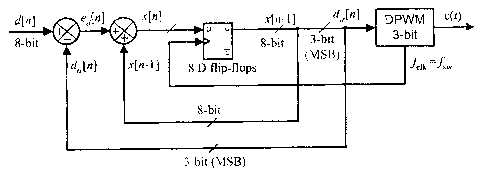
Figure 2 is a block diagram of the digital pulse with width modulator of the
present
invention based on mufti-sigma delta conversion.
Figure 3 illustrates the low-resolution core of the digital pulse width
modulator.
CA 02483378 2004-10-O1
4
Figure 4 is a dynamic model illustrating the E-0 of the digital pulse width
modulator
of the present invention.
Figure 5 is a block diagram illustrating the dual sampling/clocking mode of
the digital
controller of the present invention.
Figure 6 illustrates pulse width modulated waveforms at 60 MHz produced by ~-~
digital pulse width modulator (logic analyzer snapshot).
Figure 7 illustrates steady state operation of the digital controller of the
present
invention at 2.06 MHz switching frequency for V;"=8 V. Ch.l: Output voltage
vaut(t)
(500mV/div), Ch.2: Pulse width modulated control signal c(t) and time scale is
200ns/div.
l5
Figure 8 illustrates transient response for the load change between 0.1 and
lA, Ch.l:
Output voltage v~ut(t) (50 mV/div-ac scale), Ch. 2: load transient, and Time
scale is
100 ps/div.
Detailed Description
Fig. 1 shows block diagram of the controller of the present invention. It
combines a
novel DPWM that is in part based on a mufti-bit sigma-delta principle used in
A/D
and D/A conversions, and a novel dual-sampling/clocking control scheme to
achieve
high switching frequency, high effective resolution of the DPWM, and low power
consumption using a simple hardware.
Low-Power Digital Pulse Width Modulator Based on Mufti-Bit Sigma-Delta
Principle
Design of a high-resolution high-frequency DPWM has proven to be a challenging
task. Prior art solutions present various architectures that make design
tradeoffs
between on-chip area and power consumption, or between switching frequency
and.
the resolution of the DPWM.
CA 02483378 2004-10-O1
Conventional designs using a counter require a clock signal at a frequency
that is in
most applications significantly higher than the switching frequency and hence
generally exhibit high power dissipation when both high frequency and high
resolution are required. Designs that include a ring oscillator (delay cells)
and a
5 multiplexer have substantially lower power consumption but generally require
a large
on-chip area for the creation of high-resolution signals. Recently presented
architectures, such as hybrid, delay-Locked loop, and segmented DPWM either
combine the two previous concepts or operate with a different arrangement of
the
delay cells. These solutions demonstrate high-resolution operation (8-10 bits)
at
frequencies up to I MHz and operation with a decreased resolution at higher
frequencies. The resolution and maximum frequency of these solutions are
limited by
the propagation time, i.e. tirne step, of a delay cell and the number of cells
included in
the ring.
To improve effective resolution of the DPWM, digital dither can be introduced,
in
accordance with the prior art. However, this implementation requires use of
relatively
large look-up tables, and requires a long averaging sequence for significant
improvement of the effective DPWM resolution. In addition, for large averaging
sequences, this implementation introduces large low frequency oscillations at
the
output and as such has proven to be impractical for low power applications
The novel DPWM architecture, which we introduce here, is shown in Fig.2. It
eliminates need for a power dissipative high-frequency high-resolution DPWM
and
consequently allows power efficient operation at high switching frequencies.
The
DPWM of the present invention, which is based on the mufti-bit sigma-delta
principle, includes a high-frequency low-resolution DPWM, a delay block
(preferably
a set of D flip-flops), and two adders.
1n the specific implementation of the present invention illustrated in Fig.2,
the low-
resolution DPWM is a 3-bit unit. The system is synchronized with the clock
signal at
the switching frequency, which is produced by the low-resolution DPWM.
Figure 3 shows a low-resolution DPWM implementation in accordance with the
present invention that employs a modification of a ring-oscillator
architecture. Again,
CA 02483378 2004-10-O1
6
the system does not require an external clock signal at high frequency and
consequently has low-power consumption.
The low-resolution DPWM of the present invention is operable to vary duty
ratio of
pulse width modulated signal c(t) between eight possible discrete values: 0,
0.125,
0.25, 0.375, 0.5, 0.675, 0.75, and 0.$7S. The variations are performed over
several
switching periods to result in an average duty ratio value, which is equal to
high
resolution digital control command d[h], which in this ease is an $-bit value
(see
Fig. l). The averaging is performed by the switching converter itself, which
corner
frequency f=1/(2~c~LC) is significantly lower than fa" = 1/T~,,, where Ta,, is
the
averaging period. It should be understood that the switching converter itself
provides
elimination of high-frequency components of the mufti-bit sigma delta
modulated
signal.
1S Fast convergence toward the high-resolution value, i.e. short averaging
period, is
provided with the internal E-0 loop of the DPWM that includes tile adders and
set of
D flip-flops as shown in Fig. 2. The model of this system, which is shown in
Fig.4,
has a structure that is similar to known sigma-delta architectures. Hence,
like in other
architectures the pole at zero, i.e. at z=1 forces the average value of errors
signal to be
zero. In this case, the error e~f[n] is the difference between high-resolution
input d[n]
and the command for low-resolution DPWM dr[n]. It can be seen that high
effective
resolution of the whole structure is through simple comparison of the two
control
values, i.e. d[r~] and dt,.[n], without any additional circuitries for post-
processing of the
output value, which are usually needed in other types of sigma-delta modulated
systems.
Dynamic Nfoded of flee DPWM aid Propagation Delay
The discrete transfer function of the ~:-D DPWM, derived from the model of
Fig.3,
H~ a(z) can be written as:
H5-n(z)= C(z)= C(z) D,r(z)=z-.H (z) (1)
D(Z) D" (Z) . 1~(Z) ,aw,~,
CA 02483378 2004-10-O1
7
where, H~IH,,""(z) is the transfer function of the low resolution DPWM. It can
be seen
that the E-~1 DPWM modulation introduces additional delay of a one switching
cycle
into the transfer function of conventional DPWM.
The negative influence of this delay on a closed loop operation, i.e.
additional phase
shift and stability problems, can be minimized using control solution
described below
under the heading "Dual Sampling/Clocking Mode Controller".
Duat Sampting/Cloctcing Mode Controller
This section shows a controller suitable for the use with the previously
described
DPWM as well as wifh other low-power high-frequency configurations. It
utilizes a
dual-sampling/clocking scheme, which results in a low power consumption and in
fast
response to transients in the system.
The attenuated output voltage of the switching converter Hv~u~(t) (see Fig.l)
is
converted into its digital equivalent Hvo~,t[n] using a windowed AlD, and then
compared to the reference value Vr~~[n]. The windowed A/D produces one of only
seven possible discrete values of the errors signal a[rr.] (from -3 to +3),
based on which
the mode of the controller operation is set. The error is monitored with the
hysteretic
logic c& clock divides' block and i.f it is small, in the range of -3 to +3,
the system
operates in steady-state mode with the clock (elk 1 of Fig.S) lower than the
switching
frequency. In this mode a high resolution control value ds_,S[n] is updated
every sixth
cycle, i.e. averaging ,is performed over six switching periods, resulting in a
high
effective resolution of the ~-0 DPWM. In addition, the undersampling minimizes
power consumption and the influence of the delay of one switching cycle
introduced
by the sigma-delta modulation (1). This is because the phase shift that is
proportional
to the ratio of the delay and the sampling period is minimized when the
sampling/updating period is increased.
A block diagram of the controller is given in Fig. 5. To improve dynamic
characteristics of the system, which are limited by the steady-state mode,
dynamic
mode is introduced. The controller enters into the dynamic mode when the
hysteretic
logic recognizes an absolute error larger than 3. At that moment it changes
clock rate
CA 02483378 2004-10-O1
g
of the system, control Iaw of look-up table (LUT) based compensator, and
bridges the
internal feedback o.f the E-~ DPWM. In this mode, the fast DPWM inside the E-4
DPWM is fed by a low-resolution control value ddY[n], which is updated every
switching cycle. The controller stays in the dynamic mode until the absolute
value of
the error drops bellow 2, and then it switches back to the steady-state mode.
In steady-
state again high resolution of the pulse width modulated signal that is
necessary for
operation without limit-cycle is ensured.
Verification
The operation of the present invention is illustrated by reference to well
known
verification procedures. The present invention was implemented by operation of
a
prototype system using a low-price FPGA based development board. First a DPWM,
based on the block-diagram of Fig. 2 was constructed and then the closed loop
operation was tested.
In the implementation of the new DPWM as the low-resolution DPWM, a ring
oscillator based 3-bit DPWM was implemented. The delay cells of the low-
resolution
DPWM were constructed of D-flip-flops with typical propagation delay of 2.5
ns.
Figure 6 shows pulse-width modulated waveforms captured ~,vith a logic
analyzer,
when the control command d[n] {see Fig.2) was changing between two 8-bit
values.
It can be seen that this FPGA implementation of the new DPWM allows operation
at
constant frequency up to 60 MHz.
The results of the verification demonstrated that the architecture of the
present
invention results in a significant increase of the switching frequencies at
which digital
controllers can be used. It is reasonable to assume that by transferring this
design on
an integrated circuit that is faster than the used FPGA structure pulse width
modulated
signals at even higher frequencies (in the range of 100 MHz) could be
achieved. This
is based on implementation of the architecture to an integrated circuit in a
manner that
is known to those skilled in the art.
CA 02483378 2004-10-O1
9
Closed loop opercctior~
To further verify the operation of the controller, an experimental system
based on
block diagrams shown in Fig.l and Fig.4 was constructed. To limit the
switching
losses we designed a buck converter to operate at switching frequency of 2
MHz, and
accordingly decreased the frequency of the digital controller. To decrease the
frequency a 4-bit DPWM based on ring oscillator was implemented and each of
the
delay cells was replaced with a block of four D-flip-flops connected in
series.
The buck converter is designed to operate with input voltage that varies from
4 to
10 V, at regulated output of 3.3 V, and to supply up to 1 A of the current at
its output.
Results of the measurement of the load transient response for the output load
changes
between O.I A and 1 A are shown in Fig.B. Upon the transient the dynamic mode
was
activated with the high value of the control signal made (see Fig.S) and the
controller
quickly reduced overshoot caused by the load change. In the second phase, when
the
output voltage approached desired regulated value, the mode signal returned to
zero
value, and controller returned to steady-state mode characterized with
improved
voltage regulation. It can be seen that dual sampling technique results both
in good
output voltage regulation and fast dynamic response.
This document describes a digital controller for low-power DC-DC converters
operating at very high constant switching frequencies. A novel architecture
for a
digital pulse-width modulator based on the mufti-bit sigma-delta principle is
introduced. The new DPWM. architecture is especially suitable for on-chip
implementation. It allows creation of high-resolution high-frequency pulse-
width
modulated signals, and can be implemented with miniature low-power hardware.
The
paper also presents a new dual samplinglclocking mode control scheme that
allows
further reduction in power consumption of digital controller without penalties
in the
controller dynamic performance. Experimental FPGA-based implementation
verifies
advantages of the new architecture. Pulse width modulated signals at frequency
of 60
MHz are produced and closed loop operation of DC-DC converter operating at 2
MHz
is demonstrated.