Note : Les descriptions sont présentées dans la langue officielle dans laquelle elles ont été soumises.
CA 02484294 2004-10-29
WO 03/096454 PCT/JP03/05631
1-
DESCRIPTION
FUEL CELL ASSEMBLY, SEPARATROR-DIFFUSION LAYER ASSEMBLY FOR
FUEL CELL ASSEMBLY AND MANUFACTURING METHOD THEREFOR
TECHNICAL FIELD
The present invention relates to a fuel cell assembly. Particularly, the
present
invention relates to a compact fuel cell assembly that can be used in place of
a battery or
the like, a separator-diffusion layer assembly for such a fuel cell assembly
and a
manufacturing method therefor.
BACKGROUND OF THE INVENTION
A fuel cell comprises an electrolyte layer and a pair of catalyst carrying
electrodes (referred to as catalyst electrode layers) placed on either side of
the
electrolyte layer, and generates electricity through an electrochemical
reaction between
fuel fluid such as hydrogen or alcohol and oxidizing fluid such as oxygen or
air, which
are supplied to the corresponding catalyst electrode layers, with the aid of
the catalyst.
Figure 1 shows a conventional embodiment of a fuel cell assembly. As shown,
this fuel cell assembly 1 comprises an electrolyte layer 10, a pair of
catalyst electrode
layers 11, 12 disposed on either side of the electrolyte layer 10, a pair of
diffusion layers
13, 14 disposed on either outer side of the catalyst electrode layers 11, 12,
and a pair of
separators (or flow distribution plates) 15, 16 disposed on either outer side
of the
diffusion layers 13, 14. The separators 15, 16 can be formed by etching a
silicon
substrate, for example, and formed with channels (or recesses) 20 for defining
a flow
passage for a fuel fluid (e.g., hydrogen gas) or an oxidizing fluid (e.g.,
oxygen gas) in
their surface facing the diffusion layers 13, 14. The diffusion layers 13, 14
are provided
to diffuse the fluids evenly over the electrolyte layer 10 as well as to
contact the catalyst
electrode layers 11, 12 to thereby transmit electric potential of the
electrode layers 11,
CA 02484294 2004-10-29
WO 03/096454 PCT/JP03/05631
-2-
12 to outside, and typically formed of an electroconductive porous material
such as a
carbon paper or a carbon cloth. When the separators 15, 16 are made of an
electroconductive material or an insulating or high-resistance material
covered with an
electroconductive film, external electrodes may be attached to the separators
15, 16.
Further, in order to prevent undesirable leakage of the fluids, seal members
17, 18 are
disposed between the electrolyte layer 10 and the separators 15, 16 so as to
surround the
diffusion layers 13,14.
The fuel cell assembly l is formed by stacking these component parts and
applying a tightening force on them in the stacking direction so that the
adjacent
component parts are closely pressed to each other. For this purpose, a pair of
backing
plates 21, 22 are provided on either outer side of the separators 15, 16, a
plurality of
rods 23 extend through the backing plates 21, 22, and nuts 24 are engaged with
threaded
ends of the rods 23 so that the rotation of the nuts 24 can produce the
pressure in the
stacking direction. A required tightening pressure can be varied for different
combinations of component parts to be pressed together. However, it should be
noted
that because the diffusion layers 13, 14 made of a carbon paper/cloth or the
like have a
rough surface, a particularly large contact pressure is needed between the
diffusion
layers 13,14 and the separators 15, 16 in order to prevent the fluids from
leaking as
they pass through the diffusion layers 13, 14. Also, when the separators 15,
16 are
formed of an electroconductive material such as a metal or the surface of the
separators
15, 16 is covered with an electroconductive film to thereby allow the voltage
of the
diffusion layers 13,14 to be transmitted to outside through the separators 15,
16, it is
required to make the diffusion layers 13, 14 and the separators 15, 16 contact
each other
with a large pressure in order to reduce the contact resistance therebetween.
However, in order for the diffusion layers 13, 14 and the separators 15, 16 to
CA 02484294 2004-10-29
WO 03/096454 PCT/JP03/05631
-3-
stand the large pressure, they need to have a high mechanical strength, which
could lead
to a larger component size and/or higher manufacturing cost. Further, in the
above
structure, the tightening force applied to the separators 15, 16 and the
diffusion layers
13,14 is also imposed on other component parts which may not require such a
large
tightening pressure, and therefore these component parts also need to have a
high
mechanical strength. The large tightening force also tends to necessitate a
bulky
tightening structure (i.e., backing plates 21, rods 23 and nuts 24). These
factors can
undesirably increase the weight, volume and manufacturing cost of the fuel
cell
assembly 1.
The electrolyte of the electrolyte layer 10 may consist of a solid polymer
electrolyte (SPE). However, the SPE can function as an ion conducting membrane
only
when impregnated with water, and the SPE when impregnated with water
significantly
increases its volume. The volume of the SPE can also change depending on the
temperature. Such volume increase of the SPE can generate stress inside the
fuel cell
assembly 1. Therefore, when the externally applied tightening force is large,
the
pressure applied to the component parts may become excessively high, which can
cause
a problem such as breaking the seal members 17, 18. Controlling the pressure
at a
constant level would result in an undesirably complicated operation.
Generally, in the fuel cell assembly 1, it is preferable that the diffusion
layers
13, 14 have high electric conductivity to effectively conduct the potential of
the catalyst
electrode layers 11, 12 to outside. Also, a smaller surface roughness of the
diffusion
layers 13, 14 is preferred to lower the contact resistance between them and
the adjoining
component parts (e.g., catalyst electrode layers 11, 12 or separators 15, 16).
Further, so
long as a favorable diffusion capacity is achieved, thinner diffusion layers
13, 14 are
preferred to achieve a smaller (thinner) fuel cell assembly 1. However, in the
CA 02484294 2004-10-29
WO 03/096454 PCT/JP03/05631
-4-
conventional diffusion layers 13, 14 made of a carbon paper or carbon cloth,
there has
been a limit to the increase in the conductivity as well as reduction in the
thickness and
surface roughness.
BRIEF SUMMARY OF THE INVENTION
In view of such problems of the prior art, a primary object of the present
invention is to provide a fuel cell assembly that can eliminate the need for
applying a
large tightening pressure to the separators and the diffusion layers in the
assembled
state.
A second object of the present invention is to provide a fuel cell assembly
comprising a diffusion layer having a reduced surface roughness to thereby
decrease the
contact resistance between the diffusion layer and its adjoining component
part.
A third object of the present invention is to provide a fuel cell assembly
comprising a diffusion layer having an increased conductivity.
A fourth object of the present invention is to provide a fuel cell assembly
comprising a diffusion layer having a substantially smaller thickness than the
conventional diffusion layer while maintaining a favorable diffusing function.
A fifth object of the present invention is to provide a separator-diffusion
layer
assembly suitable for use in such a fuel cell assembly and to provide a method
for
manufacturing such a separator-diffusion layer assembly.
According to the present invention, such objects can be accomplished by
providing a fuel cell assembly (100, 200), comprising: an electrolyte layer
(110); a pair
of catalyst electrode layers (111, 112) interposing the electrolyte layer
therebetween; a
pair of separators (115, 116) each having a first surface facing the
electrolyte layer and a
second surface opposite to the first surface, the first surface of each
separator being
provided with a recess (120) through which a fuel fluid or an oxidizing fluid
flows to
CA 02484294 2004-10-29
WO 03/096454 PCT/JP03/05631
-5-
contact an associated one of the catalyst electrode layers; and a pair of
diffusion layers
(113, 114) each being disposed between the first surface of an associated one
of the
separators and an associated one of the catalyst electrode layers, wherein
each of the
diffusion layers comprises an electroconductive film (133, 133a, 133b) formed
integrally with the associated separator so as to form a separator-diffusion
layer
assembly (130,131, 130a, 203) in cooperation with the associated separator,
and
wherein each diffusion layer is formed with a plurality of fluid paths
(125,125a, 125b,
157) extending therethrough in a direction of its thickness so as to be in
flow
communication with the recess of the associated separator and thereby diffuse
the fluid
flowing in the recess over a surface of the associated catalyst electrode
layer.
Thus, by integrally forming the diffusion layer on the separator to constitute
a
separator-diffusion layer assembly, it is possible to eliminate the need for
applying a
large pressure on the diffusion layer and the separator to achieve close
contact
therebetwoen, and therefore, the tightening pressure externally applied to the
fuel cell
assembly can be considerably reduced. This can reduce the mechanical strength
required to the component parts of the fuel cell assembly to thereby decrease
the
manufacturing cost thereof. Further, the influence of the stress that may be
caused by
expansion of the electrolyte layer in operation can be moderated, which
eliminates the
need for controlling the tightening pressure and thus can simplify the
operation. The
integrated diffusion layer and the separator also result in a smaller number
of
component parts and assembly steps.
The electroconductive film of each diffusion layer can be preferably formed on
the associated separator by a process comprising physical vapor deposition
(PVD),
chemical vapor deposition (CVD), spin coating, sputtering or screen printing.
By using
such a film forming process used in a semiconductor or micromachine
manufacture in
CA 02484294 2004-10-29
WO 03/096454 PCT/JP03/05631
-6-
forming the electroconductive film of the diffusion layer, it is possible to
form a very
thin electroconductive film, which contributes to minimizing the dimension
(thickness)
of the resulting fuel cell assembly. The reduced thickness of the fuel cell
assembly is
preferred particularly when a plurality of such fuel cell assemblies are
stacked together
to form a series connection because the thickness of the resulting fuel cell
stack can be
also minimized. Further, the diffusion layers can have a high electric
conductivity when
the electroconductive film thereof is made of a highly electroconductive
material such
as a metal or an alloy.
Each separator preferably comprises a silicon substrate or a glass substrate.
The
silicon substrate or glass substrate for use in semiconductor manufacture or
the like has
a very low surface roughness, and the diffusion layer formed thereon can
readily
assume a very low surface roughness in its surface facing the catalyst
electrode layer.
This not only can reduce the contact resistance between the diffusion layer
and the
catalyst electrode layer, but also can maintain the contact resistance
substantially
constant irrespective of the tightening pressure.
The plurality of fluid paths of each diffusion layer may comprise a plurality
of
openings (125) formed in the electroconductive film of the diffusion layer
over the
recess of the associated separator. Alternatively, each diffusion layer may
comprise a
plurality of electroconductive films (133, 133a, 133b) wherein each of the
plurality of
electroconductive films is formed with a plurality of openings (125, 125a,
125b) in such
a manner that the openings of each electroconductive film are in flow
communication
with the openings of its adjacent electroconductive films) to form the
plurality of fluid
paths of the diffusion layer. When the recess of each separator extends in a
prescribed
direction, it will be preferable if the plurality of openings of the
electroconductive film
associated with each separator are arranged in a direction of extension of the
recess to
CA 02484294 2004-10-29
WO 03/096454 PCT/JP03/05631
_7_
form a line of openings in such a manner that adjacent openings in the line of
openings
partially overlap each other in a direction of extension of the line of
openings. In this
way, the recess extending along the direction of arrangement of the openings
can be
obtained without a complicated process by just etching a substrate made of an
inorganic
material such as silicon using the openings as etching windows.
In order to enhance the mechanical strength of the diffusion layers, each
diffusion layer may preferably comprise a structure reinforcement member (132)
disposed between the electroconductive film and the associated separator. In
the case
that each separator comprises a silicon substrate, the structure reinforcement
member
can consist of a silicon nitride layer or a silicon oxide layer. The plurality
of fluid paths
of each diffusion layer may comprise a plurality of openings formed in the
structure
reinforcement member of the diffusion layer. In other words, the openings in
the
structure reinforcement members can contribute to evenly diffusiing the fuel
fluid and
oxidizing fluid over the surfaces of the catalyst electrode layers. When the
recess of
each separator extends in a prescribed direction, it will be preferable if the
plurality of
openings of the structure reinforcement member associated with each separator
are
arranged in a direction of extension of the recess to form a line of openings
in such a
manner that adjacent openings in the line of openings partially overlap each
other in a
direction of extension of the line of openings. In this way, the recess
extending along
the direction of arrangement of the openings can be obtained without a
complicated
process by just etching a substrate made of an inorganic material such as
silicon using
the openings as etching windows.
According to another aspect of the present invention, there is provided a
separator-diffusion layer assembly (130,131, 130a, 203) for a fuel cell
assembly,
comprising: a separator (115, 116, 115a) having a first surface formed with a
recess
CA 02484294 2004-10-29
WO 03/096454 PCT/JP03/05631
_g_
(120) through which a fuel fluid or an oxidizing fluid flows and a second
surface
opposite to the first surface, and a diffusion layer (113, 114, 201) provided
on the first
surface of the separator, wherein the diffusion layer comprises an
electroconductive
film (133, 133a, 133b) formed integrally with the separator and is formed with
a
plurality of fluid paths (125, 125a, 125b) extending through the diffusion
layer in a
direction of its thickness so as to be in flow communication with the recess
of the
separator and thereby diffuse the fluid in the recess on a side of a surface
of the
diffusion layer facing away from the first surface of the separator.
According to yet another aspect of the present invention, a method for
manufacturing a separator-diffusion layer assembly of a fuel cell assembly,
comprising
the steps of: forming a diffusion layer (113, 114, 201) on a surface of a
substrate (150)
consisting of an inorganic material, wherein the diffusion layer has an
electroconductive
film (133, 133x, 133b) formed integrally with the substrate and is provided
with a
plurality of fluid paths (125, 125a, 125b) extending through the diffusion
layer in a
direction of its thickness; and bringing an etchant into contact with the
surface of the
substrate through the fluid paths of the diffusion layer to form a recess
(120) in the
surface of the substrate for allowing a fuel fluid or an oxidizing fluid to
flow
therethrough and whereby make a separator (115, 116, 115a).
Thus, by allowing the etchant to reach the surface of the substrate through
the
fluid paths formed in the diffusion layer, it is possible to process the
substrate and form
the recess defining a passage for the fuel fluid or oxidizing fluid without
complicated
machining. Preferably, the step of forming a diffusion layer comprises a step
of forming
the electroconductive film on the surface of the substrate by a process
comprising
physical vapor deposition (PVD), chemical vapor deposition (CVD), spin
coating,
sputtering or screen printing.
CA 02484294 2004-10-29
WO 03/096454 PCT/JP03/05631
-9-
Also preferably, the step of forming a diffusion layer may comprise the step
of
forming a plurality of openings (125) in the electroconductive film, wherein
the fluid
paths of the diffusion layer comprise the plurality of openings formed in the
electroconductive film, and the plurality of openings of the electroconductive
film are
arranged to form one or more lines of openings in such a manner that adjacent
openings
in each line of openings partially overlap each other in a direction of
extension of the
line of openings. Alternatively or in addition, the step of forming a
diffusion layer may
comprise the steps of: forming a structure reinforcement member (132) between
the
substrate and the electroconductive film; and forming a plurality of openings
in the
structure reinforcement member, wherein the fluid paths of the diffusion layer
comprise
the plurality of openings formed in the structure reinforcement member, and
the
plurality of openings of the structure reinforcement member are arranged to
form one or
more lines of openings in such a manner that adjacent openings in each line of
openings
partially overlap each other in a direction of extension of the line of
openings. In this
way, it is possible to form a recess(s) extending along the lines) of openings
of the
electroconductive film or of the structure reinforcement member can be readily
formed
in the substrate by etching.
Other and further objects, features and advantages of the invention will
appear
more fully from the following description.
BRIEF DESCRIPTION OF THE DRAWINGS
Now the present invention is described in the following with reference to the
appended drawings, in which:
Figure 1 is a schematic cross-sectional view for showing a conventional
embodiment of a fuel cell assembly:
Figure 2 is a schematic cross-sectional view for showing a preferred
CA 02484294 2004-10-29
WO 03/096454 PCT/JP03/05631
-10-
embodiment of a fuel cell assembly according to the present invention;
Figure 3 is a partial plan view of the separator-diffusion layer assembly of
the
fuel cell assembly shown in Figure 2;
Figure 4 is a schematic cross-sectional view of the separator-diffusion layer
assembly for showing an example of connection between the diffusion layer and
the
external electrode in the fuel cell assembly of Figure 2;
Figure 5 is a schematic cross-sectional view for showing another embodiment
of the separator-diffusion layer assembly according to the present invention;
Figures 6a-6d are schematic partial cross-sectional views for showing a
preferred method for manufacturing the separator-diffusion layer assembly of
the fuel
cell assembly shown in Figures 2-4;
Figures 7a-7c are schematic partial cross-sectional views for showing a
preferred method for manufacturing the separator-diffusion layer assembly of
the fuel
cell assembly shown in Figures 2-4;
Figures 8a-8e are schematic partial cross-sectional views for showing a
preferred method for manufacturing the separator-diffusion layer assembly of
the fuel
cell assembly shown in Figure 5;
Figures 9a-9c are partial plan views for showing three electroconductive films
in yet another embodiment of the separator-diffusion layer assembly according
to the
present invention;
Figure 10a is a partial plan view showing the overlapping three
electroconductive films shown in Figures 9a-9c, and Figure 10b is a cross-
sectional
view taken along the line Xb-Xb in Figure 10a;
Figures 11a-11e are schematic partial cross-sectional views for showing a
preferred method for manufacturing the separator-diffusion layer assembly of
the fuel
CA 02484294 2004-10-29
WO 03/096454 PCT/JP03/05631
-11-
cell assembly shown in Figures 9a-10b; and
Figures 12a-12d are schematic partial cross-sectional views for showing a
preferred method for manufacturing the separator-diffusion layer assembly of
the fuel
cell assembly shown in Figures 9a-10b.
DETAILED DESCRIPTION OF THE PREFERRED EMBODIMENTS
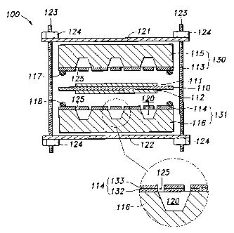
Figure 2 is a schematic cross-sectional view showing a preferred embodiment
of a fuel cell assembly according to the present invention. Similar to the
conventional
fuel assembly 1, this fuel cell assembly 100 comprises a centrally disposed
electrolyte
layer 110, a pair of catalyst electrode layers 111, 112 disposed on either
side of the
electrolyte layer 110, a pair of separators 115, 116 made of an inorganic
material such
as silicon or glass and defining fluid passages (recesses) 120 for a fuel
fluid or oxidizing
fluid in a surface facing the catalyst electrode layers 111, 112, seal members
117, 118
disposed between the electrolyte layer 110 and the separators 115, 116, and
backing
plates 121,122, rods 123 and nuts 124 for providing a tightening pressure when
assembling together the component parts. Though not shown in the drawing, the
fluid
passages 120 are each provided with a fluid ports) in its bottom for allowing
entrance
and discharge of the fluid into and out of the fluid passage 120.
This fuel cell assembly 100 differs from the conventional fuel cell assembly 1
of Figure 1 in a sense that a pair of diffusion layers 113, 114 for diffusing
the fluids
evenly over the electrolyte layer 110 as well as contacting the catalyst
electrode layers
111, 112 to transmit the electric potential of these catalyst electrode layers
111, 112 to
outside are formed integrally with the associated separators 115, 116 to
thereby
constitute separator-diffusion layer assemblies 130, 131, respectively. The
diffusion
layers 113, 114 are formed with a plurality of small openings 125 extending in
a
direction of thickness thereof so as to be in flow communication with the
fluid passages
CA 02484294 2004-10-29
WO 03/096454 PCT/JP03/05631
-12-
120 of the associated separators 115, 116 and thus diffusing the fluids in the
fluid
passages 120 over the surface of the associated catalyst electrode layers
111,112.
As shown in a partial enlarged cross-sectional view in Figure 2, each
diffusion
layer 113, 114 preferably comprises a structure reinforcement member 132
formed on
the associated separator 115, 116 and an electroconductive film 133 formed on
the
structure reinforcement member 132. When the separators 115,116 are made of
single
crystal silicon, for example, the structure reinforcement member 132 can
consist of a
silicon nitride film or silicon oxide film deposited on the surface of the
separators 115,
116. As described in detail later, the electroconductive film 133 can be
formed by a film
forming process used in a semiconductor manufacturing or micromachine
manufacturing processes such as physical vapor deposition (PVD), chemical
vapor
deposition (CVD), spin coating, etc. The small openings 125 can be formed by
patterning the structure reinforcement member 132 and electroconductive film
133 by
etching, for example.
Figure 3 is a partial plan view showing a surface (first surface) of the
separator-diffusion layer assembly 130 (131) that is formed with the diffusion
layer 113
(114). In this drawing, the diffusion layer 113 (114) is shown with a part
thereof broken
away to show the fluid passages 120 in the separators 115 (116). As shown, the
openings 125 formed in the diffusion layer 113 (114) are arranged along the
extension
of the fluid passages 120 of the separator 115 (116). Each opening 125 has an
elongated
shape and is inclined with respect to the direction of extension of the fluid
passages 120
so that the openings 125 adjoining in the direction of extension of the fluid
passages 120
partially overlap each other. It should be noted that Figure 2 shows a cross-
section along
the lines II-II in Figure 3, and thus shows two partially overlapping openings
125 over
each fluid passage 120. However, the number and position of the openings 125
shown
CA 02484294 2004-10-29
WO 03/096454 PCT/JP03/05631
-13-
in the drawing may change depending on the position at which the cross-section
is taken.
Thus, by forming the plurality of openings 125 in the diffusion layer 113
(114) so that
they are located over the fluid passages 120 to whereby supply the fuel fluid
or
oxidizing fluid in the fluid passages 120 to the catalyst electrode layer 111
(112) via the
openings 125, it is possible to diffuse the fluids evenly over the catalyst
electrode layer
111 (112). Moreover, as describe later, the openings 125 provided in the
diffusion layer
113 (114) can be preferably used as etching windows when forming the fluid
passages
120 in the separator 115 (116) by etching.
Similarly to the conventional embodiment, the fuel cell assembly 100 shown in
Figure 2 is formed by rotating the nuts 124 to thereby cause the adjoining
component
parts to closely contact with each other. However, because the diffusion
layers 113, 114
and the separators 115, 116 are unified to constitute the separator-diffusion
layer
assemblies 130, 131 as described above, there is no need to impart a large
pressure for
achieving close contact between the diffusion layers 113, 114 and the
separators 115,
116. Therefore, the tightening pressure externally applied to the fuel cell
assembly 100
can be substantially reduced. This can reduce the mechanical strength required
to the
component parts of the fuel cell assembly 100 to thereby decrease the
manufacturing
cost thereof. Further, the influence of the stress that may be caused by
expansion of the
electrolyte layer 10 in operation can be moderated, which eliminates the need
for
controlling the tightening pressure and thus can simplify the operation. The
integrated
diffusion layers 113,114 and the separators 115,116 also result in a smaller
number of
component parts and assembly steps.
The electroconductive film 133 and the structure reinforcement member 132
can be formed by a film forming process used in semiconductor or micromachine
manufacture, and therefore can be given a very small thickness, which in turn
CA 02484294 2004-10-29
WO 03/096454 PCT/JP03/05631
-14-
contributes to minimizing the size (thickness) of the fuel cell assembly 100.
The
reduced thickness of the fuel cell assembly 100 is preferred particularly when
a plurality
of such fuel cell assemblies 100 are stacked together to form a series
connection
because the thickness of the resulting fuel cell stack can be also minimized.
The
electroconductive film 133 of the diffusion layers 113, 114 can have a high
electric
conductivity when it is made of a highly electroconductive material such as a
metal or
an alloy.
Further, when the separators 115, 116 each consist of a silicon substrate or
glass substrate having a very low surface roughness such as those for use in
semiconductor devises, the diffusion layers 113,114 formed thereon can also
have a
very low surface roughness in their surface facing the catalyst electrode
layers 111, 112.
This not only can reduce the contact resistance between the diffusion layers
113, 114
and the catalyst electrode layers 111, 112, but also can maintain the contact
resistance
substantially constant irrespective of the tightening pressure.
As is well known in this art, the electric polarity of the fuel cell assembly
100
is determined by the fluids supplied to the fluid passages 120. Specifically,
the catalyst
electrode layer 111, 112 (and the diffusion layer 113, 114 contacting it)
contacting the
fuel fluid such as hydrogen (H2) constitutes an anode while catalyst electrode
layer 111,
112 (and the diffusion layer 113,114 contacting it) contacting the oxidizing
fluid such
as oxygen (O~) constitutes a cathode. As shown in the schematic diagram of
Figure 4,
external electrodes 134 may be attached to the diffusion layers 113, 114
directly.
Figure 5 is a schematic cross-sectional view showing another embodiment of
the separator-diffusion layer assembly according to the present invention. In
this
drawing, component parts similar to those in Figure 4 are denoted with the
same
numerals. In this separator-diffusion layer assembly 130a, a separator 115a
comprises
CA 02484294 2004-10-29
WO 03/096454 PCT/JP03/05631
-15-
electroconductive paths 140 passing therethrough, and an electroconductive
film 141 is
formed on a surface (outer or second surface) of the separator 115a opposite
to the
surface (first surface) on that the diffusion layer 113 is formed. The
diffusion layer 113
(more specifically, its electroconductive film 133) and the electroconductive
film 141
are connected to each other via the feedthrough conductive paths 140 whereby
the
electric potential of the diffusion layer 113 is transmitted to the
electroconductive film
141 on the outer surface of the separator 115a. This can allow the external
electrode 134
to be attached to the electroconductive film 141 on the outer surface of the
separator
115a. When the fuel cell assembly utilizes the separator-diffusion layer
assembly 130a
of Figure 5, series-connection of a plurality of such fuel cell assemblies can
be readily
achieved by just making the separator outer surfaces of adjoining fuel cell
assemblies
contact each other. The mechanically and electrically unified diffusion layer
113 and
separator 115a can remove concern about the contact resistance therebetween
and can
make the resistance constant irrespective of the degree of the tightening
pressure.
Further, the feedthrough conductive paths 140 each provides a shortest path
connecting
the diffusion layer 113 to the electroconductive film 141 on the outer surface
of the
separator 115a, to thereby contribute to minimizing the internal resistance of
the fuel
cell assembly.
Referring to Figures 6a-7c, a preferred process for manufacturing the
separator-diffusion layer assembly 130 (131) having the integrally formed
separator 115
(116) and diffusion layer 113 (114) as shown in Figures 2-4 is described
hereinafter.
First, as shown in Figure 6a, a substrate 150 consisting of single crystal
silicon
and having a thickness of about 400 ,~ m, for instance, is washed by using
sulfuric acid
or the like, and then, as shown in Figure 6b, silicon nitride films 151, 152
of about 0.2
,~ m thickness, for example, are formed on top and under surfaces of the
substrate 150
CA 02484294 2004-10-29
WO 03/096454 PCT/JP03/05631
-16-
by sputtering.
Then, as shown in Figure 6c, an electroconductive film 153 of about 2 ,u m
thickness is formed on top of the substrate 150 by physical vapor deposition
(PVD), for
example. The electroconductive film 153 can preferably have a two-layered
structure
comprising a titanium (Ti) layer 155 having a thickness of about 0.1,~ m and a
gold
(Au) layer 154 of about 2 ,cc m formed thereon. Titanium improves the contact
between
the silicon nitride and gold, and may be substituted by aluminum (Al), nickel
(Ni) or
chromium (Cr). Gold may be substituted by other electroconductive material
such as
nickel (Ni), copper (Cu), platinum (Pt), iron (Fe), tungsten (W), molybdenum
(Mo),
doped silicon or polysilicon. Also, film forming processes other than the
physical vapor
. deposition, such as chemical vapor deposition (CVD), spin coating,
sputtering or screen
printing may be used.
In the next step, as shown in Figure 6d, etching is performed on the
electroconductive film 153 to form a plurality of openings 156. Similarly to
the
openings 125 shown in Figure 3, in order to form a plurality of parallel-
extending fluid
passages 159 (Figure 7c) in the substrate 150, the openings 156 are arranged
along a
direction of extension of each fluid passage 159 (a direction vertical to the
sheet of
Figure 6d) to form lines of openings 156. The openings 156 each have an
elongated
shape and are inclined with respect to the direction of arrangement of thereof
so that in
each line of openings 156, adjoining openings 156 overlap each other in the
direction of
arrangement. In the cross-sectional view of Figure 6d, two openings 156
overlapping
each other in the direction of arrangement are shown in a similar fashion as
in Figure 2.
Subsequently, as shown in Figure 7a, reactive ion etching (RIE) using CF4 is
conducted with a mask (not shown) to form a plurality of small openings 157 in
the
silicon nitride film 151 on the top surface of the substrate 150 at positions
aligned with
CA 02484294 2004-10-29
WO 03/096454 PCT/JP03/05631
-17-
the openings 156 of the electroconductive film 153. The openings 157 can serve
as
etching windows for forming the fluid passages 159 (Figure 7c). Similarly to
the
openings 156 of the electroconductive film 153, the openings 157 each have an
elongated shape and are inclined with respect to the direction of arrangement
thereof so
that in each line of openings 157, the ends of the adjoining openings 157
overlap each
other in the direction of arrangement.
Further, as shown in Figure 7b, similar etching is performed with a mask (not
shown) to remove portions of the silicon nitride film 152 on the underside of
the
substrate 150 where fluid ports 160 (Figure 7c) for allowing entrance and
discharge to
and from the fluid passages 159 provided in the substrate 150 are to be
formed.
Finally as shown in Figure 7c, the substrate 150 is wet etched using an alkali
solution such as KOH solution to whereby form the fluid passages 159 and fluid
ports
160. Since this process is anisotropic etching, the side wall of each fluid
passage 159
and fluid port 160 inclines at an angle reflecting the crystal orientation of
the silicon. It
should be noted that because the openings 157 of the silicon nitride film 151
on the top
surface of the substrate 150 are arranged in a direction of extension of the
fluid passages
159 and the openings 157 adjoining in the direction of arrangement partly
overlap each
other, a continuous fluid passage 159 can be preferably formed under each line
of
openings 157. Thus, the separator-diffusion layer assembly 130 (131) as shown
in
Figures 2-4 is obtained. As will be understood, the openings 156,157 in Figure
7c
correspond to the openings 125 in Figures 2-4. Also, the upper silicon nitride
film 151
functions as the structure reinforcement member 132 shown in the enlarged view
in
Figure 2.
Next, with reference to Figures Sa-Se, a preferred process for manufacturing
the separator-diffusion layer assembly 130a having the feedthrough conductive
paths
CA 02484294 2004-10-29
WO 03/096454 PCT/JP03/05631
-18-
140 is described hereinafter. In these drawings, portions similar to those in
Figures
6a-7c are denoted with the same numeral and detailed explanation thereof is
omitted.
After forming the silicon nitride films 151, 152 on either surface of the
silicon
substrate 150 in the step of Figure 6b, etching is conducted with a mask (not
shown) to
remove portions of the silicon nitride film 151 on top of the substrate 150
where
feedthrough conductive paths 162 (Figure 8d) are to be formed, as shown in
Figure 8a.
Then, in the step shown in Figure 8b, the electroconductive film 153 is formed
on top of the substrate 150 by vapor deposition, spin coating or the like. As
in the above
embodiment, the electroconductive film 153 preferably has a two-layered
structure
comprising the gold layer 154 and the titanium layer 155.
Next, after etching is performed with a mask (not shown) to remove portions of
the silicon nitride film 152 on the underside of the substrate 150 where the
feedthrough
conductive paths 162 (Figure 8d) are to be formed, wet etching is performed
with an
alkali solution such as KOH solution to form through holes 161 reaching the
electroconductive film 153 covering the top surface of the silicon substrate
150. Since
this process is also anisotropic etching, the side wall of each through-hole
161 inclines
at an angle reflecting the crystal orientation of the silicon such that the
cross-section of
each through-hole 161 diverges from the top to under surface of the substrate
150 (or
from the first to second surface of the separator 115a).
Subsequently, as shown in Figure 8d, metallic material is deposited from
underside the substrate by vapor deposition or the like to form
electroconductive films
162, 163, each of which preferably have a two-layered structure comprising a
titanium
layer adjoining the substrate 150 and a gold layer adjoining the titanium
layer, on the
side wall of the through-holes 161 and on the under surface of the substrate
150,
respectively. The metallic material is also deposited on the underside of the
CA 02484294 2004-10-29
WO 03/096454 PCT/JP03/05631
-19-
electroconductive film 153 covering the upper opening of the through-holes
161, and
thus the electroconductive film 153 and the electroconductive film 162 on the
side wall
of the through-holes 161 are connected to each other. It should be noted that
since the
side wall of each through-hole 161 is inclined as described above, the
deposition of the
metallic material thereon is facilitated so that the sufficiently thick and
uniform
electroconductive film 162 on the side wall can be preferably achieved. It
should be also
noted that in the step shown in Figure 8c, dry etching or other process may be
used
instead of wet etching to form the through-holes 161 having a vertical side
wall. In such
a case, however, forming the electroconductive film 162 uniformly on the side
wall
could become more difficult than in the case where the through-holes 161 are
formed by
wet etching.
Thus, the electroconductive film 162 on the side wall of each through-hole 161
connects the electroconductive film 153 on top of the substrate 150 and the
electroconductive film 163 on the underside of the same. In other words, the
electroconductive film 162 on the side wall of each through-hole 161 functions
as the
feedthrough conductive path 140 shown in Figure 5. Thereafter, the steps shown
in
Figures 6d-7c are carried out similarly, whereby the fluid passages 159, fluid
ports 160,
etc. are formed as shown in Figure 8e, providing the separator-diffusion layer
assembly
130a having the feedthrough conductive path 140 (electroconductive film 162)
as
shown in Figure 5.
In the above embodiments, the diffusion layer 113 (114) has only a single
electroconductive film 133 (153) formed with the openings 125 (156). However,
it is
possible to stack a plurality of patterned electroconductive films to provide
a diffusion
layer with complicated fluid paths that can achieve more even diffusion of the
fluids.
For example, it is possible to form second and third electro conductive films
133a, 133b
CA 02484294 2004-10-29
WO 03/096454 PCT/JP03/05631
-20-
on the electroconductive film 133 of the separator-diffusion layer assembly
130 (131)
shown in Figure 2 to provide a separator-diffusion layer assembly 203
comprising a
diffusion layer 201 having three electroconductive films 133, 133a and 133b.
Figures 9a-9c show an example of patterning of the electroconductive films
133, 133a and 133b. Figure 9a is substantially the same as Figure 3 and shows
the shape
and arrangement of the openings 125 of the electroconductive film 133 together
with
the fluid passages 120 of the separator 115 (116). As shown in Figure 9b, in
this
embodiment, the second electroconductive film 133a comprises openings 125a of
which
inclination angle with respect to the direction of extension of the fluid
passage 120 is
different from that of the openings 125 of the first electroconductive film
133, while as
shown in Figure 9c, the third electroconductive film 133b is formed with
openings 125b
in the same shape and arrangement as the openings 125 of the first
electroconductive
film 133.
Figure 10a is a plan view showing the electroconductive films 133, 133a and
133b stacked together, while Figure 10b shows a cross-sectional view taken
along the
line Xb-Xb in Figure 10a. As seen in these drawings, the openings 125 of the
first
electroconductive film 133 are in flow communication with the openings 125b of
the
third electroconductive film 133b via the openings 125a of the second
electroconductive
film 133a to whereby form fluid paths extending through the thickness of the
diffusion
layer 201. Each opening 125a of the second electroconductive film 133a is in
flow
communication with a plurality of openings 125 of the first electroconductive
film 133
and with a plurality of openings 125b of the third electroconductive film 133b
so that
the fluid paths assume a complicated labyrinth structure, and thus the fuel
fluid or
oxidizing fluid in the recess 120 of the separator 115 (116) is favorably
diffused over
the catalyst electrode layer 111 (112) through the fluid paths.
CA 02484294 2004-10-29
WO 03/096454 PCT/JP03/05631
-21-
In the following, with reference to the schematic drawings of Figures 11a-11e
and Figures 12a-12d, a preferred method of manufacturing the above shown
separator-diffusion layer assembly 203 having a multiple electroconductive
films is
described. In these drawings, portions corresponding to those in Figures 6a-7c
are
denoted with same numerals.
First, according to the steps described above with reference to Figures 6a-7a,
the silicon nitride films 151, 152 are formed on either side of the silicon
substrate 150,
the electroconductive film (first electroconductive film) 153 containing the
gold layer
154 and titanium layer 155 is formed on top thereof, and the first
electroconductive film
153 and the silicon nitride film 151 are patterned by etching or the like to
form a
plurality of openings 156, 157, respectively, as shown in Figure 11a.
In a step shown in Figure 11b, a sacrifice layer 258 consisting of silicon
oxide
(Si02), for example, is formed to fill in the openings 157 of the upper
silicon nitride
film 151 and the openings 156 of the first electroconductive film 153 with the
sacrifice
layer 258.
Further, after forming a resist 259 on the sacrifice layer 258 as shown in
Figure
11c, the resist 259 and the sacrifice layer 258 are etched by dry etching
until the top
surface of the first electroconductive film 153 is exposed, to thereby flatten
the top
surface.
Then, by using the steps as described above, a second electroconductive film
153a is formed on the flattened top surface, and patterned to form a plurality
of
openings 156a, as shown in Figure 11e. Further, by the steps similar to those
shown in
Figures 11b-11d, the openings 156a of the second electroconductive film 153a
is filled
with a sacrifice layer 258a, a resist (not shown) is formed thereon, and
etching is
conducted to flatten the top surface (Figure 12a).
CA 02484294 2004-10-29
WO 03/096454 PCT/JP03/05631
-22-
Further, after a third electroconductive film 153b is formed and patterned to
form openings 156b by again using the above-described steps, etching is
performed to
remove the sacrifice layer 258 filling in the openings 157 of the silicon
nitride film 151
and the openings 156 of the first electroconductive film 153 as well as the
sacrifice
layer 258a filling in the openings 156a of the second electroconductive film
153a, as
shown in Figure 12b. This brings the openings 156, 156a, 156b of the
electroconductive
films 153, 153a, 153b as well as the openings 157 of the silicon nitride film
151 into
flow communication so that the flow paths extending through the diffusion
layer 201 is
formed.
Finally, as shown in Figure 12d, the silicon substrate 150 is wet etched by
using a I~OH solution to form the fluid passages 159 and fluid ports 160, to
thereby
obtain the unitary separator-diffusion layer assembly 203. In this step, the
etchant can
reach the surface of the silicon substrate 150 through the openings 156, 156a,
156b of
the electroconductive films 153, 153x, 153b as well as the openings 157 of the
silicon
nitride film 151 that form the fluid paths extending through the diffusion
layer 201.
Thus, the etching of the substrate 150 can be favorably carried out even with
the
unitarily formed diffusion layer 201.
Although the present invention has been described in terms of preferred
embodiments thereof, it is obvious to a person skilled in the art that various
alterations
and modifications are possible without departing from the scope of the present
invention which is set forth in the appended claims. For instance, though in
the above
embodiments the deposited electroconductive film is patterned by etching, an
electroconductive film having a predetermined pattern can be also obtained by
photolithography, lift-off, etc. Also, in the above embodiments, the
electroconductive
film and the structure reinforcement member of the diffusion layer formed
integrally
CA 02484294 2004-10-29
WO 03/096454 PCT/JP03/05631
-23-
with the separator are provided with a plurality of openings arranged along
each fluid
passage (recess) of the separator such that the opening each have an elongated
shape
and are inclined with respect to the direction of arrangement thereof.
However, the
shape of the opening can vary in a variety of ways, and may have a V-shape or
W-shape,
for example. In such cases also, it is preferred that the openings adjoining
in the
direction of arrangement partially overlap each other because fluid passages
extending
along the direction of arrangement of the openings can be readily obtained by
etching
the separator using such openings as etching windows.
INDUSTRIAL APPLICABILITY
As described above, according to the present invention, the diffusion layer of
the fuel cell assembly comprises an electroconductive film integrally formed
with the
separator so that the separator and the diffusion layer constitute a unitary
separator-diffusion layer assembly. This can eliminate the need for applying a
large
external pressure for making the separator and the diffusion layer closely
contact with
each other. This also reduces the pressure applied on other component parts in
the fuel
cell assembly, decreasing the required mechanical strength and the
manufacturing cost.
The integrated diffusion layer and the separator also reduce the number of
component
parts and manufacturing steps. Further, by forming the electroconductive film
using a
film forming process used in a semiconductor or micromachine manufacture, it
is
possible to achieve a very thin diffusion layer comprising the
electroconductive film,
which contributes to minimizing the dimension (thickness) of the resulting
fuel cell
assembly.