Note : Les descriptions sont présentées dans la langue officielle dans laquelle elles ont été soumises.
CA 02484320 2004-10-08
ACTIVE COHERENCE REDUCTION FOR
INTERFEROMETER INTERROGATION
BACKGROUND OF THE INVENTION
Field of the Invention
The present invention relates to interferometric optical sensor systems
employing active coherence reduction of the source light.
Description of the Related Art
The coherence function of an optical signal versus delay z and time t is
defined as the autocorrelation function of the normalized field phasor E(t) of
the
optical signal. In other words, the coherence function R(z,t) equals the
autocorrelation function of the light and is given by
r+ 2
R(i,t) _ ~E*(t')E{t'+i)w(t'-t)dt' (1 )
r_T
z
In the common mathematical definition of the coherence function the
integration time
T in equation (1 ) approaches infinity, while w(t) is independent on t and
equals 1IT.
If two optical field phasors E(t) and E(t+z) originating from the same saurce
with
delay difference ~ are combined on a detector, the visibility of the
interference signal
output from the detector will be proportional to the magnitude of an effective
coherence function R(z,f), which is still given by equation (1 ), but where
w(t) equals
the impulse response of the detector. If w(t) also includes the effect of
electrical or
digital receiver filters attached to the detector output, R(z,t) describes the
visibility of
the output signals from the receiver filters. In equation (1 ), w(t)
represents a moving
average weighting function that is multiplied with the interference power term
E*(t')E(t'+z) . Normalization of the field phasor E(t) means that the field
phasor is
scaled such that R(O,t) = 1 on the average.
It can be shown that the coherence function of the light can be defined as the
Fourier transform of its optical power spectrum. The coherence time may be
defined
as the full width at half maximum (FWHM) of the autocorrelation function, and
it can
1
CA 02484320 2004-10-08
be shown that the coherence time is inversely proportional to the bandwidth of
the
optical power spectrum. The term "coherence length" is used for the distance
that
the ligh-t will travel within the coherence time. The effective coherence
function
discussed above can be defined as the Fourier transform of the optical power
spectrum after convolution with the Fourier transform of w(t). This
corresponds to
taking the Fourier transform of the optical power spectrum measured with
resolution
bandwidth that corresponds to the bandwidth of w(t), i.e. the detector
bandwidth.
The effective coherence time is then the full width at half maximum (FWHM) of
the
effective autocorrelation function, and the effective coherence length is the
distance
that the light will travel within the effective coherence time.
In most practical interferometric applications it is the effective coherence
function, where w(t) equals the impulse response of the detector including
filters,
that is of interest, and in the following we use the terms coherence function,
coherence time, and coherence length when we mean the effective coherence
function, effective coherence time, effective and coherence length.
Interferometric optical sensor systems will typically comprise an optical
source unit, which produces an optical signal. If wavelength division
multiplexing of
sensor interferometers is employed, this signal may typically comprise a
multiple of
optical signals, each signal being confined to a separate wavelength range
defining
a wavelength channel. Such a multiwavelength channel source may typically
comprise a multiple of laser sources operating in different wavelength
channels, and
a wavelength division multiplexer arranged to combine the different wavelength
signals. If time division multiplexing of sensor interferometers is employed,
the
optical signal from the source unit may typically comprise pulses.
The optical signal from the source unit is launched into an optical network
comprising a multiple of optical pathways from its input to its output, and
where
some pairs of optical pathways form sensor interferometers. The difference in
delay
between two paths forming a sensor interferometer is called the sensor delay
or
imbalance of that sensor. The optical network may typically use optical
waveguides
such as optical fiber for guiding of the optical signals. If wavelength
division
multiplexing is employed the optical network may typically comprise wavelength
dependent couplers or wavelength dependent reflectors such as fiber Bragg
grating
2
CA 02484320 2004-10-08
(FBG) reflectors, arranged in a manner such that optical signals belonging to
a
wavelength channel will only propagate through a limited set of the paths
through
the network. Thus, different sensors can be interrogated with light in
different
wavelength channels.
Light emerging from the output of the optical network is typically directed to
a
detection unit. If wavelength division multiplexing is employed the detection
unit
may typically comprise a wavelength division demultiplexer which separates the
different wavelength channel components of the incoming light and directs the
separated components to corresponding wavelength channel detectors. The
detectors will typically convert the incoming light signals to output voltage
or current
signals that are proportional to the optical power.
The electrical signals emerging from the signal processing unit will typically
be analyzed by some signal processing means to extract information dependent
on
the phase of the sensor interferometers, defined as the difference in phase
delay
experienced by the interrogating optical signal when traveling in the two arms
of a
sensor interferometer. The phase of a sensor interferometer is linearly
dependent
on the exact sensor delay of the interferometer. This information may
typically carry
useful information about physical parameters acting differently on the two
pathways
comprising each sensor interferometer. Examples of such physical parameters
are
acoustic vibrations or pressure fluctuations, temperature, or hydrostatic
pressure.
Some sensor interferometers may also be designed to be insensitive to physical
parameters that one wants to measure, and rather be used as reference sensors
to
correct the readout from other sensor interferometers for influences from
physical
parameter fluctuations that one does not want to measure, but which affect the
measurements from both the reference sensor and the corrected sensor. The
signal
processing means may typically comprise components such as analog mixers,
sample and hold circuits, analog to digital converters, microprocessors,
digital signal
processors, etc.
The sensor system may also comprise a compensating interferometer. A
compensating interferometer comprises two optical paths from its input to its
output
with a path imbalance, i.e. difference in transmission delay between the two
paths,
that is chosen to be approximately equal to that of the path delay of the
sensor
3
CA 02484320 2004-10-08
interferometer. The compensating interferometer is connected in series with
the
sensor interferometer, either after the source unit at the optical transmitter
end (in
which case it is called a transmitter interferometer in parts of the existing
literature)
or before the detector unit at the receiver end (in which case it is called a
receiver
interferometer in parts of the existing literature).
The compensating interferometer ensures that there will be for each sensor
interferometer a pair of pathways from the source unit to the detection unit
going
through both the compensating interferometer and the optical network (with the
compensating interferometer placed either before or after the optical network)
that
has a delay imbalance that is close to zero, i.e. much shorter than the sensor
interferometer delay. Since the sensitivity of the interference phase to
source
frequency fluctuations is proportional to the delay imbalance of the optical
pathways
that the interfering waves have traveled, the use of a compensating
interferometer
can allow for the use of cheaper light sources with a lower optical frequency
stability
or phase stability and lower coherence, as opposed to systems that do not
employ
compensating interferometers. The level of frequency fluctuations that can be
allowed is decided by the production uncertainty or spread in the mismatch
between
the compensating interferometer delay difference and the sensor interferometer
delay differences. For fiber optic interferometric sensor systems this spread
can
depend on uncertainties in the fiber splicing process and fiber strain levels,
as well
as in some cases the flexibility of placement of fiber splices within the
sensor
housing. The uncertainty can typically be in the range of 1 to 50 mm in fiber
length,
corresponding to delay variations in the order of 0.01 to 0.5 ns for a dual
path fiber in
a reflector-based interferometer. In sensor systems comprising compensating
interferometers, pairs of pathways with delay imbalances close to one and two
times
the sensor interferometer delay will also exist. Interference between light
components with such delay imbalances can lead to nonlinear responses and
noise
in the sensor readout. In pulsed multiplexed systems, these interference terms
are
removed by pulsing of the source with pulses that are shorter than the sensor
interferometer delay, resulting in that the wanted interference between pulse
components that have experienced approximately equal delays from the source
unit
to the detection unit will be separated in time from pulse components that
have
experienced unequal delays. The wanted interference signal can thus be
separated
and extracted by time gating or discrete time sampling of the output signals
from the
4
CA 02484320 2004-10-08
detection unit. Due to the pulsed nature of the interrogation signals such
systems
can readily be adapted for time division multiplexing (TDM). Sensors belonging
to
different TDM channels will then have different offset transmission delays
from the
source unit to the detection unit, so that detected interference signals from
the
different sensors can be separated in the time domain by time gating or
discrete
time sampling of the output signals from the detection unit.
Various approaches have been disclosed for extracting the sensor phase.
Most of them rely on varying the interference phase of the sensor
interferometers
actively as a function of time through modulation of the phase or frequency of
the
interrogating optical signal or by modulation of the interferometer imbalance.
This
ensures that the signal processing means can extract both in-phase and
quadrature
information about the interference of each sensor interferometer by analyzing
the
output signals from the detection unit as a function of time, thus enabling
the
interference phase to be extracted without sign ambiguity. One may for example
employ the "phase generated carrier" (PGC) demodulation approach disclosed in
the Homodyne Demodulation Scheme for Fiber Optic Sensors Using Phase
Generated Carrier by A. B. A. Dandridge et al. published in IEEE J. of Quantum
Electronics, Vol. QE-18, pp. 1647-1653, 1982, wherein the term PGC refers to
the
carrier frequencies generated at the detector at the frequency at which the
interference phase is actively modulated and at harmonics of this frequency.
The
sensor interferometer phase can be extracted without sign ambiguity by
analyzing
the detector signals in a frequency band comprising minimum two of the
generated
frequencies. The interference phase modulation can be generated in several
ways,
for instance by modulation of the optical source frequency, modulation of the
optical
phase or frequency outside the source, or by modulating the delay in one of
the
interferometer arms. If a compensating interferometer is employed,
interference
phase modulation can be generated by modulation of the phase delay in one of
the
arms of the compensating interferometer. Systems where the optical signal
component traveling in one of the pathways of a sensor interferometer is
frequency
shifted relatively to the optical signal component traveling in the other
pathway of the
same sensor interferometer may also be used to generate a heterodyne signal at
the detector, as described in U.S. Patent No. 6,466,706 entitled "Pulsed
System and
Method for Fiber Optic Sensor," resulting in a carrier signal at the detector
onto
which the sensor interferometer phase is encoded and can be extracted without
sign
5
CA 02484320 2004-10-08
ambiguity. For most of the demodulation approaches based on the PGC or
heterodyning techniques, PGC frequencies or optical frequency shifts,
respectively,
that are at least larger than two times the readout frequency bandwidth of the
demodulated sensor phase signal are required to avoid frequency overlap of the
detected carrier sidebands and to avoid nonlinearities and errors in the
demodulated
output signals.
Phase demodulation without sign ambiguity can also be achieved without any
modulation of the interference phase or generation of carrier frequencies at
the
detectors. For instance, a compensating interferometer placed in front of the
detection unit with outputs from a 3x3 fiber coupler to two or three detectors
may be
used, as disclosed for a pulsed system in U.S. Patent No. 5,946,429 entitled
"Time-
Division Multiplexing of Polarization-Insensitive Fiber Optic Michelson
Interferometric
Sensor." The interference signals at the outputs from the 3x3 coupler will
then be
phase shifted relative to each other, thus providing both in-phase and
quadrature
information about the interference signal to the signal processing means.
The detection unit has a detector bandwidth that is capable of capturing ail
the information required by the signal and processing unit to demodulate the
sensor
interferometer phase with the required demodulated phase signal bandwidth.
With
PGC demodulation techniques the necessary detection bandwidth may typically
include from 2 to 12 harmonics of the PGC frequency. With heterodyne
demodulation techniques the necessary detection bandwidth may typically be in
the
order of one to two times the heterodyne frequency shift. With demodulation
techniques employing a 3x3 fiber coupler in front of the detection unit, the
necessary
detection bandwidth may typically be in the order of one to a few times the
required
demodulated phase signal bandwidth. Due to nonlinearities in the interference
phase to fringe signal response, even higher detection bandwidths may be
required
if the demodulated phase signal amplitude is high.
In systems employing a pulsed optical source the necessary detection
bandwidth must be sufficient to avoid unwanted crosstalk in the time domain
between subsequent pulses, and the necessary detection bandwidth will
typically be
in the order of the inverse of the pulse duration, i.e. the inverse of the
sensor
interferometer delay.
6
CA 02484320 2004-10-08
Additional components may also be included in the interferometric sensor
system, such as for example optical amplifiers to boost the optical power
emerging
from the source unit before it is launched into the system, polarization
controllers,
power supplies, optical circulators, optical modulators for modulating the
sensor
interferometer phase, and more.
Interferometric sensor systems employing pulsed sources with a coherence
length that is even shorter than the pulse length in combination with
compensating
interferometers are known from the prior art. Due to the pulsed nature of the
interrogation signals such systems can readily be adapted for time division
multiplexing. Pulses with duration shorter than the interferometer imbalance
are
generated by the source. The fraction of a pulse that follows the short path
through
the sensor interferometer and the long path through the compensating
interferometer will then overlap at the detector with the fraction of the same
pulse
that follows the long path through the sensor interferometer and the short
path
through the compensating interferometer.
In most of the prior art references employing short coherence sources, a
coherence time that is shorter than the pulse length is achieved through
inherent
random processes in the source such as spontaneous emission or thermal
radiation.
However, such random processes correspond to random fluctuations in the source
frequency or phase. If the compensating interferometer delay is not perfectly
matched to the sensor interferometer delay, these random frequency
fluctuations will
cause unwanted noise fluctuations in the readout phase, as discussed above.
The
'706 patent discloses an alternative approach where the optics! field phasor
(i.e. the
complex field amplitude) of the light emerging from a coherent source is
modulated
in a controlled and repetitive manner by chirping the optical frequency within
each
pulse delivered by the source unit with an acoustooptic modulator. This
ensures
that the mean optical frequency of the source is not disturbed from pulse to
pulse,
and thus conversion from source frequency fluctuations to noise in the
demodulated
sensor phase signal is avoided. The minimum coherence time that can be
achieved
by coherence modulation using this technique is limited by the response time
or the
duration of the impulse response of the modulator, which is fundamentally
limited by
the speed of sound in the acoustooptic interaction medium to the range from 5
to
100 ns for high speed modulators, and the price and complexity of the
modulators
7
CA 02484320 2004-10-08
increases with increasing speed. This imposes a limit to how much the
coherence
time can be reduced by this technique, and thus a limit to how much the
unwanted
effects of the source coherence, which are discussed below, can be suppressed.
The use of low coherent sources provides several advantages, including
reduced noise, crosstalk and harmonic distortion in the sensor response from
interference with unwanted reflections such as Rayleigh scattering,
reflections from
other sensors multiplexed on the same fiber, connectors, etc. Essentially,
only
reflectors that are separated from the sensor reflectors by less than the
coherence
length of the source will contribute to errors in the demodulated signal.
If the lead fiber is of substantial length, distributed Rayleigh scattering
may
cause a significant amount of noise at the detectors and thus in the
demodulated
sensor interferometer phase signals. It can be shown that the squared Rayleigh
noise contribution to the detector signal output is proportional to,
1 ~~R(z,t)f adz (2)
2Tf -Tf
where Tf is the transmission delay through the fiber contributing with
Rayleigh noise
to the demodulated phase signal. It is thus desirable to get the integral
expression
in (2), which represents a Rayleigh noise suppression factor, as small as
possible. If
the coherence function has only one peak versus ~, the integral will be
directly
proportional to the coherence time.
In systems employing pulsed interrogation, reflections with delay spacing
from the interferometer that equals a multiple of the interrogation pulse
period will
interfere with the sensor reflections. If subsequent pulses are correlated
with a
stable or slowly varying phase relation, such reflections will contribute to
crosstalk
and harmonic distortion. If subsequent pulses are not correlated and the pulse
phase relation varies in a random fashion such reflections will contribute to
noise in
the demodulated phase signal. In systems employing a common down lead and up
lead fiber any losses in the lead fiber, due to for instance connector losses
or
directional couplers, will reduce the ratio of the reflected signal pulse
amplitudes
from the sensor interferometers to unwanted reflections from higher up in the
lead
8
CA 02484320 2004-10-08
fiber. Interference with unwanted reflections can therefore significantly
degrade the
quality of the demodulated readout signal.
As already mentioned, the combination of a compensating interferometer and
a low coherence source reduces the requirements on the source frequency
stability,
since the readout phase is proportional to the product of the optical source
frequency and the delay imbalance of the interfering pulses. For example, in a
system with a sensor interferometer delay of ~ = 100 ns (corresponding to 20 m
of
single pass delay in optical fiber), a readout phase resolution of ~~ = 1 mrad
requires that the source frequency has fluctuations less than ~~/(2~~) = 160
Hz
within the demodulated bandwidth of interest if a compensating interferometer
is not
used. This requires advanced and expensive laser sources that must be isolated
from vibrations. When a compensating interferometer that matches the sensor
interferometer within 0~ = 0.1 ns (20 mm fiber) is used, the source frequency
stability
requirements are relaxed by three orders of magnitude to o~/(2na~) = 160 kHz.
Due
to uncertainties in fiber strain and in the fiber splicing process involved it
is hard to
achieve delay matching better than the order of 0.01 to 0.5 ns.
The use of low coherence sources also increases the threshold for unwanted
Brillouin scattering in systems employing long lead fibers to reach remote
sensor
locations. The optical input power required to overcome shot noise limitations
of the
detector (receiver) can be high, especially if optical losses are high. In
such cases,
the input optical power required to overcome shot noise may exceed the
threshold
for stimulated Brillouin scattering (SBS) if a highly coherent source is
launched into a
long lead fiber. If the SBS threshold is exceeded; a large fraction of the
optical
input signal is scattered by phonons, which are generated due to the high
optical
power. This causes a large reduction of the optical power reaching the sensor
(effective loss). If a common optical fiber is used for transmission to and
from the
sensor (as in reflective sensor systems) SBS will lead to a large signal
superimposed on the reflected sensor response. Instabilities in the SBS
process
may also cause severe noise in the readout signal. Acceptable system
performance
can therefore not be achieved when the SBS threshold is exceeded.
Provided that the fiber transmission loss is less than a few dB, in a
monochromatic optical source, the SBS threshold power is inversely
proportional to
9
CA 02484320 2004-10-08
the lead fiber length. For higher losses (assuming a given attenuation per krn
and
increasing fiber length), the threshold power approaches a constant level. If
the
bandwidth BW of the source exceeds the gain bandwidth of the SBS process,
which
for silica fiber may be in the range of BWsBS=20 to 100 MHz, then the SBS
threshold will also be proportional to the bandwidth ratio BWIBWsBS, where BW
is
the optical bandwidth of the source. More precisely, the threshold condition
is
determined by the peak of the optical power spectral density of the source
averaged
with an optical resolution bandwidth of BWsBS. BWsss depends on the lifetime
of
the stimulated phonons in the fiber.
Some prior art references exist where the coherence function of the source is
synthesized to have a peak at a chosen delay by modulating the source field
phasor
in a periodic manner, either by modulating the drive current of a source laser
or by
use of an external modulator. Peaks in the coherence function will then occur
at
multiples of the modulation period. In U.S. Patent No. 4,818,064 entitled
"Sensor
Array and Method of Selective Interferometric Sensing by Use of Coherence
Synthesis," this technique is used to select to which interferometer among a
multiple
of sensor interferometers with different sensor delay imbalances that the
demodulation should be sensitive. By varying the modulation period sensors
with
different delay imbalances can be selected. This type of coherence synthesis
provides some of the same advantages with respect to suppression unwanted
effects of Rayleigh and other spurious reflections as well as stimulated
Brillouin
scattering as other techniques employing low coherence sources for
interferometric
sensor interrogation. However, since the coherence function becomes a periodic
function of delay with a repetition period equal to the sensor interferometer
delay,
the readout will be sensitive to Rayleigh and spurious reflections that
introduces
pathways from the source unit to the detection unit that is spaced by any
multiple of
the sensor interferometer delay from the transmission delays of the sensor
interferometer paths. In other words, the Rayleigh noise suppression factor as
defined in equation (2) will contain unwanted contributions from a large
number of
coherence peaks. For comparison, the pulsed source unit described in the '706
patent will have a coherence function with peaks that repeat for every pulse
repetition interval, which is typically much longer than the sensor delay.
Another
shortcoming of the technique disclosed in the '064 patent is that the
sensitivity to
CA 02484320 2004-10-08
fluctuations in the mean source frequency (i.e. laser frequency fluctuations)
is much
higher than for systems employing a compensating interferometer.
In general, interferometer interrogation techniques employing continuous
wave and pulsed sources have different advantages and disadvantages that make
them preferable for different applications. Pulsed source interrogation allows
for
time division multiplexing in addition to wavelength division multiplexing,
and may
therefore be advantageous for systems where multiplexing of a large number of
interferometers is required. On the other hand the short dutycycle of the
detected
interference pulses means that rather high optical pulse powers are required
to
overcome the fundamental shot noise limitation of optical detection. This can
be
overcome by increasing the source power, for instance by incorporating a
relatively
expensive optical amplifier. However, in sensor systems with long transmission
lead
fibers to the sensor location and in addition possible significant
transmission losses
near the sensors the power requirement may become so high that nonlinear
processes like self phase modulation and Raman power transfer, cross phase
modulation, or four wave mixing and between wavelength channels may lead to
problems by introducing excess noise and effective loss mechanisms to the
transmitted optical signal. Furthermore, the pulsed approach requires very
high
speed components which may be relatively expensive such as high speed
intensity
modulation means for switching and high speed detection and sampling
electronics.
For low cost systems that do not require time division multiplexing of too
many
sensors and for systems where transmission losses and lead fiber lengths are
large,
continuous wave systems may thus provide an advantage over pulsed systems.
Thus, there exists a need for improved techniques for interrogation in
interferometric sensor systems employing pulsed sources that reduce readout
interferometer phase errors to Rayleigh scattering, spurious reflections, or
stimulated Brillouin scattering, and which overcomes other problems with the
prior
art mentioned herein. There exists a further need for improved techniques for
interrogation in interferometric sensor systems employing continuous wave
sources
that reduce readout interferometer phase errors caused by Rayleigh scattering,
spurious reflections, or stimulated Brillouin scattering, and which overcomes
other
problems with the prior art mentioned herein.
11
CA 02484320 2004-10-08
SUMMARY OF THE INVENTION
The present invention generally applies to an interferometric sensor system
that may comprise optical waveguides such as optical fibers, and other optical
components such as optical waveguide couplers and optical circulators. The
interferometric sensor system also comprises an optical source unit that
produces
light in at least one wavelength channel. The fight from the optical source
unit is
launched into an optical network comprising a multiple of optical pathways
from the
source unit to the detection unit, where pairs of optical pathways form sensor
interferometers, each sensor interferometer having a sensor delay difference
similar
to a nominal sensor delay. One of the optical pathways of a first sensor
interferometer may be sensitive to a physical measurand such as acoustic
vibration
or acoustic pressure fluctuation, while another sensor interferometer may be
insensitive to the physical measurand, thus forming a reference sensor
providing
information for correction of the measurement made by the first sensor
interferometer. The optical network may comprise a multiple of optical
wavelength
selective reflectors such as fiber Bragg gratings or optical wavelength
selective
couplers to enable wavelength division multiplexing of the sensor
interferometers.
The light received from the optical network is converted to electrical signals
using a
detection unit, and processing means are applied to the electrical signal to
extract
information dependent on the phase of the sensor interferometers.
The invention provides a method for reducing noise and harmonic distortion
due to unwanted reflection such as Rayleigh scattering, reflections from other
sensors multiplexed on the same fiber, connectors, etc. The invention also
provides
a method that increases the threshold for Stimulated Brillouin Scattering
(SBS).
This enables more optical power to be launched into the optical network, when
the
optical power of the source is limited by SBS. The reduction of noise and
harmonic
distortion and the increase of the SBS threshold are achieved by reducing the
coherence of a highly coherent optical source by coherence modulation means
that
modulates the output field phasor of each channel to produce a broadened
optical
source power spectrum.
The coherence modulation means reduces the autocorrelation of the source,
where the autocorrelation function of a wavelength channel is defined as the
Fourier
12
CA 02484320 2004-10-08
transform of the optical source power spectrum in one wavelength channel,
where
the optical power spectrum is defined with a resolution bandwidth similar to
the
necessary detection bandwidth. Alternatively, the autocorrelation function of
a
wavelength channel from the source versus delay may be defined as a filter
impulse
response convolved with the product of the conjugate of output field phasor
and the
output field phasor delayed by the given delay, where the filter impulse
response
has a frequency representation with a bandwidth similar to the necessary
detection
bandwidth. The coherence time may be defined as the full width at half maximum
(FWHM) of the autocorrelation function. The coherence time is inversely
proportional to the bandwidth of the optical source power spectrum. An
efficient
coherence modulation means for use in combination with a compensating
interferometer will produce an output field phasor with a coherence time that
is
significantly shorter than the sensor delay. If the coherence time is
sufficiently short,
signal components that appear due to interference formed between optical
pathways, with a delay different from the sensor delay of the interrogated
interferometer, will be substantially suppressed. If a compensating
interferometer is
not used, significant improvements can still be achieved by reducing the
coherence
time from that of a highly coherent laser source to a coherence time that is
reduced
but longer than the sensor interferometer delay, without disturbing the mean
source
frequency.
It is essential that the coherence modulation means produce an
autocorrelation function that is stable versus time. if this is not the case,
noise will
be added on the signal from sensors with sensor delays that are not completely
matched with the maximum of the autocorrelation function. The stability of the
autocorrelation function within the necessary detection bandwidth can be
achieved
by modulating the output field phasor of each wavelength channel from the
source in
a periodic manner with a cycle frequency that is larger than the necessary
detection
bandwidth. Alternatively, stability of the autocorrelation function can be
achieved by
modulation of the output field phasor of each wavelength channel from the
source in
a periodic manner with a cycle frequency that is phase-locked to a
demodulation
carrier frequency, such as the phase generated carrier (PGC) modulation
frequency
in a system employing PGC demodulation or the heterodyne frequency in a system
employing heterodyne demodulation.
13
CA 02484320 2004-10-08
In an embodiment, the source unit produces a continuous wave output or
pulses with a duration that is different from the nominal sensor delay. A
compensating interferometer is formed with two optical pathways from its input
to its
output that have a delay difference that is equal or substantially similar to
the
nominal sensor delay. The compensating interferometer is arranged in a
serially
coupled manner with the optical network. This compensating interferometer may
either be placed between the source unit and the optical network or between
the
network and the detection unit: In this configuration, the compensating
interferometer balances the delays of the sensors, and the phase of the sensor
can
be extracted from an interference signal formed between two optical pathways
that
have a delay difference that is close to zero. Large unwanted signal
components
may also appear due to interference formed between optical pathways with a
delay
difference close to one and two times the sensor delay. The optical source
unit
must therefore produce an optical signal with an autocorrelation function that
is
substantially reduced for delays close to one and two times the sensor delay,
but
close to a maximum for delays within a spread of the deviation of the delay
differences of the sensor interferometers from the delay difference of the
compensating interferometer.
Coherence modulation means that produces a broadened optical spectrum
may be achieved by direct modulation of the source laser for each wavelength
channel. If the source laser is a fiber laser, direct modulation can be
achieved by
periodic strain modulation of the fiber laser. If the source laser is a diode
laser,
direct modulation can be achieved by periodic modulation of the drive signal
of the
diode laser, and the modulation signal may have triangular waveform. If the
source
laser is a wavelength tunable diode laser, direct modulation can be achieved
by
periodic modulation of one or more control signals to the wavelength tunable
diode
laser, and the laser wavelength may have triangular waveform. A triangular
waveform provides a more uniform spread of the optical spectrum than a pure
sine
modulation, and thus more confined peak in the coherence function with less
sidelobes.
Coherence modulation means that produces a broadened optical spectrum
may also be achieved by using an optical modulator that takes light output
from at
least one coherent fight source as input and modulates the field phasor of the
light
14
CA 02484320 2004-10-08
before it is output from the modulator. Light from a multiple of coherent
light sources
operating at different wavelength channels may be combined with a wavelength
division multiplexer and input to a common optical modulator, which modulates
all
wavelength channels simultaneously. This may provide a more cost effective
solution than to use one modulator for each wavelength source. The optical
modulator may be one out of an optical phase modulator, an optical amplitude
modulator or an acousto-opticaP modulator. An optical phase modulator may
comprise an optical fiber wound around a piezoelectric rang modulator, for
example a
lead titanate zirconate (PZT) ring modulator. In order to reduce polarization
effects,
the optical fiber may be twisted High Birefringence fiber or polarization
maintaining
fiber, where the input polarization to the polarization maintaining fiber is
polarized
along one of the polarization maintaining fiber eigenaxes. The optical phase
modulator may also be an electro-optical phase modulator such as a lithium
niobate
phase modulator. Lithium niobate phase modulators have the advantage of a much
higher speed than most other types of optical modulators, and much shorter
coherence lengths can therefore be achieved with such a device than with for
example an acousto-optic modulator. The phase modulator may modulate the
phase of the output field phasor of each wavelength channel with a repeated
pseudorandom pattern switching between two phase-shift values that are
separated
by ~ radians. Other modulation patterns may also be employed. For a PZT ring
modulator a sine modulation at a mechanical resonance frequency of the PZT
ring
may be desirable.
In another embodiment, the optical source unit produces pulses with duration
similar to the nominal sensor delay in at least one wavelength channel. A
sampling
unit samples the output electrical signals from the detection unit at time
instances
when a detected signal arising from interfering portions of one of the
received light
pulses having propagated the pair of optical pathways forming a sensor
interferometer arrives at the sampling unit. A compensating interferometer
with
optical pathways from its input to its output is formed with a delay
difference that is
equal to or substantially similar to the nominal sensor delay that is arranged
in a
serially coupled manner with the optical network. The compensating
interferometer
may either be placed between the source unit and the network or between the
network and the detection unit. Coherence modulation means that produces a
broadened optical spectrum is achieved using an electro-optic phase modulator
CA 02484320 2004-10-08
such as a lithium-niobate modulator. Lithium niobate phase modulators have the
advantage of a much higher speed than most other types of optical modulators,
and
much shorter coherence lengths can therefore be achieved with such a device
than
with for example an acousto-optic modulator. The phase modulator may
preferably
modulate the phase of the output field phasor of each wavelength channel with
a
repeated pseudorandam pattern switching between firvo phase-shift values that
are
separated by ~c radians.
BRIEF DESCRIPTION OF THE DRAlI111NGS
So that the manner in which the above recited features of the present
invention can be understood in detail, a more particular description of the
invention,
briefly summarized above, may be had by reference to embodiments, some of
which
are illustrated in the appended drawings. It is to be noted, however, that the
appended drawings illustrate only typical embodiments of this invention and
are
therefore not to be considered limiting of its scope, far the invention may
admit to
other equally effective embodiments.
Figure 1 is a schematic illustration of an interferometric sensor system
employing continuous wave interrogation comprising a coherence modulator and a
compensating interferometer.
Figure 2 is a schematic illustration of a single path coherence modulator
employing a lead titanate zirconate modulator.
Figure 3 is a schematic illustration of a dual path coherence modulator
employing a lead titanate zirconate modulator and a Faraday rotation mirror.
Figure 4 is a schematic illustration of an interferometric sensor system
employing pulsed interrogation comprising a coherence modulator and a
compensating interferometer.
Figure 5 is an illustration of a pseudorandom drive signal with abrupt
transitions applied to the coherence modulator.
Figure 6 is an illustration of a pseudorandom drive signal with rounded
transitions applied to the coherence modulator.
16
CA 02484320 2004-10-08
DETAILED DESCRIPTION OF THE PREFERRED EMBODIMENT
The combination of a low coherence source and a compensating
interferometer may also be used in systems employing continuous wave (CW)
source interrogation rather than pulsed source interrogation, if a
compensating
interferometer is used in combination with a phase generated carrier (PGC)
technique, the PGC cannot be induced by modulating the source directly.
However,
it may be induced by a phase modulator placed in one of the arms of the
compensating interferometer, or by modulation of the optical frequency of the
light
between the output of the compensating interferometer and the input to the
lead
fiber. The PGC can also be generated by modulating the delay in one of the
interferometer arms, provided that these positions are accessible.
A basic idea of the present invention is to modulate the complex field
amplitude of the signal interrogating an optical interferometer in such a way
that the
temporal coherence is reduced, thus reducing the sensitivity to unwanted
reflections
with time delays that are different from the sensor reflector. In the
following we will
name this "coherence modulation" of the interrogation signal. The coherence
modulation can be represented mathematically by multiplication of a coherent
optical
field phasor in the time domain with a complex "coherence modulation
function".
The coherence modulation function should preferably not be random, but should
have a form that ensures that the demodulated sensor signal has a low
sensitivity to
the coherence modulation. This can be achieved by ensuring that the mixing
product of the coherence modulation function and other modulation functions
(pulsing, phase modulation, PGC generation, heterodyne frequency shifting,
etc.)
imposed on the interrogating signal does not produce mixing products at the
detector that are within the necessary frequency band required by the
demodulation
process.
In a system employing CW interrogation and a compensating interferometer
the coherence modulation can be introduced by placing a coherence modulator
with
input from the output of a laser source. The laser should preferably have a
moderate level of frequency noise. This is illustrated in Figure 1 for the
case where
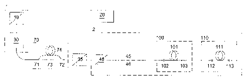
the compensating interferometer 70 is placed between the source unit 1 and the
optical network 2 comprising the interferometric sensors. Light from the laser
source
17
CA 02484320 2004-10-08
passes thorough the coherence modulator 30 before it exits the source unit 1
and
enters the compensating interferometer, which here is illustrated as a Mach-
Zender
interferometer comprising an input coupler 71, a short arm 73, a long arm 74,
and an
output coupler 72. The output from the compensating interferometer is sent
through
5 a frequency modulator 35, which is responsible for generating the PGC
modulation,
and into the down lead fiber 45, typically via a directional coupler or
circulator 40.
The down lead fiber propagates the light to the sensor interferometer. Instead
of the
device 35 there are alternative ways of generating the PGC modulation, for
instance
by placing a phase modulator in one of the arms of the compensating
interferometer
10 70. In Figure 1, the sensor interferometer is illustrated as a Fabry-Perot
type
interferometer 100 employing two weak fiber Bragg Grating (FBG) reflectors 102
and 103 with typically < 5 % power reflectivity at the source wavelength. To
achieve
matching of the compensating and the sensor interferometer delays, the length
of
sensor fiber 101 should equal %2 times the length of the length difference
between
the long 74 and the short 73 fiber of the compensating interferometer.
The use of wavelength selective FBG reflectors in the sensor interferometer
allows for wavelength division multiplexing (WDM) of multiple sensors,
exemplified
in the figure by a second sensor interferometer 110 with FBGs 112 and 113 that
reflects light in a wavelength channel different from the FBGs 102 and 103 of
the
first interferometer. In the wavelength multiplexed configuration the source
10
should combine light from multiple sources, each source emitting within one of
the
WDM channel wavelengths. The detector unit 20 should comprise a WDM
demultiplexer that splits the different sensor wavelengths to different
detectors. The
electrical signal generated at each detector is processed, for instance by any
known
technique in the art to extract the sensor phase of that wavelength channel.
The coherence modulator 30 could typically be a phase modulator operating
at a frequency far above the PGC modulation frequency generating a phase
amplitude » 1 rad. In a typical application the PGC frequency could be 20 kHz
and
the coherence modulation frequency could be 1 MHz.
The phase modulator used for the coherence modulation can be formed as
illustrated in Figure 2 by winding a length of fiber (typically 5 to 20 m)
around a
piezoelectric, preferably PZT (lead titanate zirconate), cylinder 50
(typically with 2
18
CA 02484320 2004-10-08
mm wall thickness) with electrodes 51 and 52 at the inner and outer surface of
the
cylinder, and modulating the voltage between the electrodes with a sine signal
at the
coherence modulation frequency, which should preferably be selected to match a
radial acoustic resonance in the cylinder.
A PZT phase modulator like the one illustrated in Figure 2 may typically
induce polarization modulation on the interrogating signal due to the
transverse
force modulating the birefringence on the fiber that is wound on the PZT ring.
One
approach for reducing this problem may be to use a high birefringence or
polarization maintaining (PM) fiber on the PZT and to ensure that the input
polarization to the PM fiber is aligned with one of the fiber eigenaxes. This
can be
achieved, for example, by using PM fibers and components in the optical path
from
the source to the coherence modulator, or by placing a polarizer at the input
to the
PM fiber that is aligned with one of the axes of the PM fiber and using
polarization
controllers to ensure maximum transmission for each wavelength channel through
the polarizer.
The PZT phase modulator in Figure 2 may also be replaced by an electro-
optic phase modulator, for instance a Lithium-Niobate (LiNiob) phase
modulator.
The phase shift in such commercially available LINiob modulators can typically
be
modulated only by one or a few n radians. The phase modulator may modulate the
phase of the output field phasor of each wavelength channel with a repeated
pseudorandom pattern switching between two phase-shift values that are
separated
by ~ radians. By a pseudorandom sequence we generally mean a signal sequence
that is synthesized, not truly random, and that has reduced coherence
properties
with minimal sidelobes outside the coherence peak at zero delay. If the
pseudorandom pattern is repeated periodically there will also be coherence
peaks at
every delay multiple of the repetition period. One example of pseudorandom
sequences is the maximal sequences described in "Spread Spectrum Systems with
Commercial Applications," 3'd edition, by Robert C. Dixon, Willey & Sons,
1994.
Other modulation patterns may also be employed. The minimum phase switching
interval of this sequence should preferably be much shorter than the sensor
interferometer delay. LiNiob phase modulators have the advantage of a much
higher speed than most other types of optical modulators, and much shorter
coherence lengths combined with a better coherence sidelobe suppression can
19
CA 02484320 2004-10-08
therefore be achieved with such modulators than with for example an acousto-
optic
modulator. Since most available LiNiob phase modulators are polarization
sensitive,
one typically has to ensure that the input polarization to the modulator is
aligned with
one of the modulator's eigenaxes. As described in the previous paragraph, this
can
be achieved for example by use of PM fibers and components all the way from a
polarized source to the modulator, or by a combination of polarization
controllers
and a polarizer in front of the modulator.
The effect of the polarization modulation induced by a PZT phase modulator
can be reduced by implementing the modulator 30 as illustrated in Figure 3
with a
dual path reflective device employing a PZT cylinder 62 and Faraday rotating
mirror
65. Light from the laser source 10 is guided through the input fiber 31 via a
coupling
device 60 to the modulator fiber 61 which is wound around the PZT cylinder 62
with
electrodes 63, 64. The polarization state of the light is rotated 90°
by the Faraday
rotating mirror 65 and is reflected back through modulator fiber 61 to the
coupling
device 60, which directs the light to the modulator output fiber 32. The
coupling
device 60 can typically be an optical circulator or an ordinary 3-dB coupler.
The
output fiber 32 is further connected to the compensating interferometer 70 in
Figure
1. Due to the polarization rotation property of the Faraday mirror the
polarization
state at the output fiber 32 should be independent on the birefringence
modulation
imposed by the PZT, provided that the birefringence modulation is slow
compared to
the optical transit time of the fiber wound on the PZl- ring 55 plus the fiber
length
between the PZT ring and the Faraday mirror 52.
The interfering light reflected from the sensor in Figure 1 is propagated back
through the up-lead fiber 46, which may typically be identical to the down-
lead fiber
45, and guided to the detection unit 20. If the down-lead and the up-lead
fibers are
identical, the returned signal may be split off from this common lead fiber by
the
coupler or circulator 40, as illustrated in Figure 1.
For each sensor there will exist four different pathways in Figure 1 denoted
a,
b, c, and d (not labeled) from the source to the detector, going through:
a: the short reference interferometer arm and the short sensor
interferometer arm
CA 02484320 2004-10-08
b: the short reference interferometer arm and the long sensor
interferometer arm,
c: the long reference interferometer arm and the short sensor
interferometer arm,
d: the long reference interferometer arm and the long sensor
interferometer arm.
The interferometer formed by paths b and c will cause interference with high
visibility
at the detector, since delay imbalance is nominally zero. Interferometers
formed by
the path pairs a-b, a-c, b-d, and c-d will all have an imbalance close to or
equal to
the sensor delay, and the interference visibility of these interferometers
will be
proportional to the autocorrelation of the coherence modulation function
evaluated at
the sensor delay. The interferometer formed by the two paths a and d will have
an
imbalance close to two times the sensor delay, and the interference visibility
of this
interferometers will thus be proportional to the autocorrelation of the
coherence
modulation function evaluated at two times the sensor delay. , To minimize
nonlinearities in the sensor readout response and to minimize sensitivity to
source
frequency fluctuations, the autocorrelation of the coherence modulation
function
evaluated at the sensor delay and at two times the sensor delay should be made
as
small as possible. This can be achieved by using a high phase modulation
amplitude in a PZT coherence modulator (which reduces the average amplitude of
the autocorrelation function). It can also be achieved by adjusting both the
amplitude and shape (distribution of harmonics) of the coherence modulation
function to minimize the absolute value of the autocorrelation function at the
two
delays involved.
It may also be an advantage to use a periodic coherence modulation signal
where the coherence modulation signal is phase locked to a harmonic of the PGC
signal. If periodic sampling of the detector signals or of signals derived
from these
signals is used in the demodulation process, it may also be an advantage to
phase
lock the coherence modulation signal to a harmonic of the sampling frequency.
Similarly, in any sensor system employing some type of heterodyne
interferometric
demodulation technique it may be an advantage to phase lock the coherence
modulation signal to a harmonic of the heterodyne frequency. Such phase
locking
21
CA 02484320 2004-10-08
should ensure that aliasing or mixing between harmonics of the PGC, heterodyne
and/or sampling frequency will mainly contribute to the demodulated phase
signal
near DC, which may be an advantage if the sensor is used for AC measurements.
Coherence modulation can also be achieved by direct modulation of the
frequency and/or amplitude modulation of the source. For example, the
frequency
of a fiber distributed feedback laser can be modulated by modulating the
strain in the
fiber, for instance by stretching it with a piezoelectric actuator. The
frequency and
amplitude of a semiconductor laser can be modulated by modulating the laser
drive
current. Approaches using direct source modulation may seem attractive, since
fewer components are required than for the external modulation approach
discussed
above. A potential problem with approaches employing direct modulation of a
laser
source for coherence reduction may be to maintain a stable shape of the
coherence
function versus delay and a sufficiently stable optical frequency at low
fluctuation
frequencies. Such instabilities will lead to increased noise contributions
from
interfering terms with imbalance equal to one and two times the interferometer
delay. If the delays of the compensating and the sensor interferometers are
not
perfectly matched, it will also lead to noise in the high visibility
interference of the
compensated combined interferometer formed by paths b and c defined above.
It should be emphasized that variants of the coherence modulation technique
described above also can be applied to CW interrogated interferometric sensor
systems that do not use the PGC technique for the interrogation. For instance,
a
compensating interferometer with outputs from a 3x3 coupler to two or three
detectors may be used to provide both in-phase and quadrature information
about
the interference signal to the demodulation processing system. In such systems
the
coherence modulation must be imposed on the optical interrogating signal
before it
enters the sensor interferometers.
A PZT modulator similar to the one shown in Figure 2 can also be used for
the PGC modulator; since phase modulation is equivalent to frequency
modulation
(the optical frequency shift is 1/(2~) times the time derivative of the
optical phase
shift). Because the PGC frequency is typically much smaller than the coherence
modulator frequency, the PZT cylinder used for PGC generation may typically be
operated near an acoustic hoop resonance rather than a wall thickness
resonance.
22
CA 02484320 2004-10-08
Active coherence reduction techniques similar to the ones described above
may also be applied to systems employing continuous wave interrogation without
any compensating interferometer. One embodiment of such a version of the
present
invention may be similar to the embodiment shown in Figure 1, but without the
compensating interferometer 70. It is then essential that the coherence
modulation
function is designed such that coherence function of the optical output from
the
source unit within a wavelength channel is close to a maximum for delays close
to
the sensor interferometer delay. To ensure low noise in such a system that
does not
employ any compensating interferometer it is essential that the mean frequency
of
the source for each wavelength channel is stable. In a preferable
implementation
this can be achieved to a high degree by the use of acoustically and thermally
isolated and/or stabilized single frequency fiber Er-doped distributed
feedback (DFB)
lasers may with active feedback to a 1480 mm fiber pigtailed diode pump laser
from
an intensity noise monitor detector. The coherence length of such a laser will
typically be in the order of 10 km or more. If long lead fibers are used this
can result
in severe problems with Rayleigh scattering induced noise and stimulated
Brillouin
scattering, unless coherence reduction is applied. Coherence reduction can
preferably be achieved by the use of a PZT phase modulator similar to the ones
illustrated in Figures 2 and 3 and discussed in the previous paragraphs. To
avoid
that the coherence modulation imposes unwanted fluctuations in the output
electrical
signals from the detection unit the coherence modulation frequency should
preferably be substantially above the necessary detection bandwidth required
for the
demodulation processing. The phase modulation amplitude should preferably be
smaller than the optimum modulation amplitude for CW systems that do comprise
compensating interferometers, as to ensure that the produced coherence length
is
longer than the sensor interferometer delay.
An interferometric sensor system employing pulsed interrogation may also
benefit from active coherence reduction. Figure 4 illustrates such a system
comprising a coherence modulator and a compensating interferometer. The
illustrated components of the system may be essentially similar to the
corresponding
components illustrated in Figure 1 for a CW interrogated system, except that
an
optical switch 12 responsible for generating light pulses with a duration
similar to the
sensor interferometer delay is inserted into the source unit. The required
detection
bandwidth of the detection unit 20 must also be higher than for a CW
interrogated
23
CA 02484320 2004-10-08
system, and a time gating or discrete time sampling unit will typically be
employed to
separate and extract interference pulse signals at the detector output for
input to the
processing unit. The switch 12 may preferably be of the lithium niobate Mach
Zender type, which is available commercially from several manufacturers. The
modulator 35 may preferably be a lithium niobate phase modulator that
modulates
the phase of every second pulse emerging from the compensating interferometer
70
to create a heterodyne modulation subcarrier on the detected interference
pulses.
In Figure 4, the switch is placed between the laser source 10 and the
coherence
modulator 30, but it may also be placed between the coherence modulator 30 and
the output of the source unit 1.
The coherence modulator 30 may comprise an acousto-optic modulator that
chirps the output optical frequency in a periodic manner. As discussed in the
introduction section to this application, the minimum coherence time that is
achievable by the use of such a modulator is limited to approximately the
range from
5 to 100 ns. If an even shorter source coherence time is required it will be
more
preferable to use coherence modulation means that have a higher speed, such as
an electro-optical phase modulator. Commercially available electro-optical
phase
modulators of the lithium niobate type can have response times below 0.1 ns,
and it
may therefore be preferable to employ this type of modulator for the coherence
modulation. A preferable modulation signal may be a phase switching pattern
that
switches the optical phase between two values that are separated by ~c radians
in a
pseudorandom fashion.
Other high speed modulators such as for example electro-optical amplitude
modulators including lithium niobate Mach Zender modulators may also be used
for
the coherence modulation. In particular, it may be useful to use a chirp free
or low
chirp Mach Zender modulator. In a chirp free Mach Zender modulator the phase
in
the two Mach Zender arms are modulated in a push-pull manner. By "push-pull"
we
mean that the two phases are modulated with nominally equal amplitudes and
opposite sign. The modulator may have an input electrode with applied voltage
V~
that is coupled to the waveguides in such a way that the phase in the two Mach
Zender arms are modulated by a~V~/(4V,~) rad and -~V~I(4Vn) rad, where Vn is
often
called the half wave voltage of the modulator. Alternatively, the modulator
may have
two input electrodes that are driven with voltages of opposite sign V~ and -V~
to
24
CA 02484320 2004-10-08
achieve nominal phase shifts in the two arms of ~cV~l(4Vn) rad and -~V~I(4V~)
rad. In
both cases, the optical output field will be multiplied by a multiplier M - K
sin(r~V~l(2Vn)+8o), where 8o is the bias phase of the modulator and K is a
complex
number that depends on the insertion loss and phase delay of the device. By
the
terms chirp free or low chirp we mean that the phase of K does not change much
in
response to modulation of the drive signal V~. Most commercial chirp free Mach
Zender modulators have a separate bias electrode, and the voltage of this
electrode
should preferably be adjusted until Ao = 0. The multiplier M may thus be
changed
between -K and +K via zero by changing V~ between +V~ and -V~. The coherence
modulation is implemented by modulation of V~ between +Vn and -V.~ in a
pseudorandom fashion white the pulse is transmitted through the modulator.
Figure 5 illustrates an idealized pseudorandom drive signal for modulation of
pulses with 500 ns duration. The drive signal changes state only at 10 ns
intervals,
and the switching between the states is abrupt. If a chirp free Mach Zender
modulator is used, +1 and -1 on the vertical axis correspond to drive voltages
of +V~
and -V~, respectively. If a phase modulator is used, +1 and -1 correspond to
phase
shifts of 0 and ~c, respectively. With abrupt switching, as illustrated in
Figure 5, the
cases with the two types of modulators are equivalent. The coherence
modulation
will then ensure a coherence function that has a low value in the full delay
range
from -500 ns to 500 ns, except for a sharp triangular peak in the delay
interval from
-10 ns to 10 ns. Suppression of sidelobe peaks in the coherence function can
be
further optimized by apodization of the pulse power near the edges and by
apodization of the detector impulse response w(t).
Due to the triangular shape of the coherence peak, the visibility of the
interference signals received from a sensor will decrease linearly with the
deviation
of the sensor delay from the compensating interferometer delay. In practical
systems the sensor delays may vary, for instance due to production
uncertainties,
and in some applications a resulting uncertainty in the interference
visibility may lead
to undesirable errors in the demodulated and demultiplexed signals. Another
undesirable effect is that the sensitivity of the demodulated signal to noise
in the
coherence modulation drive signal in general increases with the reduction of
the
visibility. A coherence function that has a more rounded or parabolic shape
near its
top may therefore be desirable.
CA 02484320 2004-10-08
One way to achieve a more rounded maximum in the coherence function is
by rounding or low-pass filtering of the drive signal to the coherence
modulator, as
Illustrated in Figure 6. This works with both types of modulators, but when a
phase
modulator is used, sidelobes will grow up in the coherence function when the
phase
transitions are rounded. This is undesirable in many applications since
interference
noise arising from spurious reflectors that are positioned at delays from the
sensor
reflectors that correspond to the coherence sidelobe delay or multiples of the
pulse
repetition period pluslminus the coherence sidefobe delay will not be
suppressed
effectively by the coherence modulation. When a chirp free or low chirp Mach
Zender modulator is used, the magnitude of coherence sidelobes will not grow
when
the transitions in the modulation drive signal is rounded, and the desirable
flat
sidelobe characteristics of an ideal (not rounded) pseudorandom sequence is
maintained. This is true provided that all positive transitions from -Vn to
+V,~ have
the same shape, and that the negative transitions from +Vn to -Vn are
identical to
the positive transitions except for the change of sign. A person skilled in
mathematical signal analysis may understand this based on the following
reasoning.
The multiplier M applied to the optical field may be represented by the
constant K multiplied with an abruptly switching pseudorandom sequence like
the
one in Figure 5 and convolved with a rounding filter impulse response with a
maximum duration of 10 ns. (In general the maximum duration equals the minimum
delay between transitions in the abruptly switching pseudorandom sequence.) It
can
then be shown that the coherence function of the modulated light equals the
convolution of the coherence function of the abruptly switching pseudorandom
sequence with the coherence function of the rounding ffter impulse response..
Another potential advantage of using a chirp free Mach Zender modulator for
the coherence modulation is that the modulator can also act as the switch that
generates the pulses by setting the drive voltage to the off-state (V~ = 0) in
between
pulses. Alternatively, if a separate intensity modulator with limited switch
extinction
is used to shape the pulses before they enter the coherence modulator, the
extinction ratio of the pulses can be improved by setting V~ = 0 between the
pulses.
A further potential advantage is that apodization of the pulse power can be
implemented by reducing the peak-to-peak drive voltage amplitude towards the
ends
of the pulse, i.e. apodization of the pulse power envelope.
26
CA 02484320 2004-10-08
it is also possible to use coherence modulation employing high speed
modulation components such as lithium niobate modulators for interrogation of
interferometric sensor systems employing pulsed interrogation but not
comprising
any compensating interferometer.. A preferable implementation of such a system
may be similar to that illustrated in Figure 4, except that the compensating
interferometer 70 is not included, and the output from the source unit 1 is
directed
directly to the input of the optical network 2. In this case the optical
switch
generates two optical pulses, both with a duration similar to or less than the
sensor
interferometer delay and a separation that essentially equals the sensor
interferometer delay. Alternatively, the optical switch may generate a single
pulse
with a duration similar to two times the sensor interferometer delay. Within
the pulse
duration of the one or two pulses, the coherence modulator 30 generates two
identical modulation patterns, for example two identical pseudorandom phase
modulation sequences, that are separated in time by the sensor interferometer
delay. This output pulse pattern is repeated periodically from,the source
unit, and
the modulator 35 modulates the phase of the second half of each pulse pattern
emerging from the source unit to create a heterodyne modulation subcarrier on
the
resulting detected interference pulses.
Like for the CW system that does not employ any compensating
interferometer, a TDM system without any compensating interferometer also may
require that the mean frequency of the source for each wavelength channel is
stable
to avoid excess noise in the demodulated sensor signal. In a preferable
implementation this can be achieved to a high degree by the use of
acoustically and
thermally isolated and/or stabilized single frequency fiber Er-doped
distributed
feedback (DFB) lasers with active feedback to a 1480 mm fiber pigtailed diode
pump
laser from an intensity noise monitor detector.
Although the invention has been described and illustrated with respect to
exemplary embodiments thereof, the foregoing and various other additions and
omissions may be made therein and fihereto without departing from the spirit
and
scope of the present invention. For example, and not by way of limitation, any
or all
of the above embodiments may be used as a sensor system having a sensing
device for sensing pressure, force, seismic forces, temperature or strain. In
addition,
any or al( of the above embodiments may be used as an optical control system
27
CA 02484320 2004-10-08
having an optical filter (or resonator) device and either a passive
filterlresonator (i.e.
not tunable) or a tunable filterlresonator (e.g. in which a load is applied to
the device
to tune it, or the device is heated with a variable heating element, causing
it to
expand or shrink and so tuning it).
While the foregoing is directed to embodiments of the present invention, other
and further embodiments of the invention may be devised without departing from
the
basic scope thereof, and the scope thereof is determined by the claims that
follow.
28